40W原理图(LED驱动)
- 格式:pdf
- 大小:181.83 KB
- 文档页数:1

Powerint INN3468C+TMIMX102U DER636 40W LED驱动器解决方案Powerint公司的40W多输出反激转换器是四个LED驱动器,采用InnoMuxTMIMX102U和InnoSwitchTM3-MX INN3468C,由于不需要升压和降压转换器级而极大地改善了系统效率.它还简化开发和制造多个输出的电源. InnoSwitch3-MX架构是革命性,在单个IC器件集合了初级和次级控制器,高压功率开关,以及检测元件和安全的反馈机制. InnoSwitch3-MX初级控制器是准谐振(QR)反激控制器,能工作在连续导通模式(CCM),采用可变电流控制方案.初级包含抖动振荡器,磁耦合次级控制器的接收器电路,限流控制器, PR IMA RY BYPASS引脚上的5V稳压器,可听噪音降噪引擎,旁路过压检测电路,无损耗输入检测电路,限流的选择电路,过压保护,前沿消隐,次级输出二极管/SR MOSFET短路保护电路以及650 V / 725 V /750 V功率开关. InnoSwitch3-MX是和InnoMux控制器配对.它是LED背景光控制器,消除了降压和LED背景光升压转换器,有一个或两个恒压输出,单独调整输出,瞬态响应±5% CV,典型输出电压,一个CV模式为5V到22V,两个CV模式为5V和12V到22V,1-4串LED背景光,LED串的匹配精度为3%,高达100V串电压/高达960mA 总串电流,高达2:1 LED串行电压范围.对所有输出有单独的过载保护,串不平衡/短路/开路保护以及输出过压设定用于自动重起.采用nnoMuxTM IMX102U和InnoSwitchTM3-MX INN3468C的40W多输出反激转换器采用独特的单级转换,多个输出和反激架构,通用90 VAC到265VAC电压输入,能源之星8.0效率兼容,5V/3A CV输出,LED串电压范围30V到50V,可配置成模拟调光模式,直接PWM调光模式,滤波PWM调光模式以及混合调光模式.本文介绍了InnoSwitch3-MX产品亮点,典型应用/性能图,初级框图和次级框图,以及InnoMux产品亮点, 控制器功能框图,采用nnoMuxTM IMX102U和InnoSwitchTM3-MX INN3468C的DER 636 40W多输出反激转换器主要特性和指标,电路图,材料清单和PCB设计图.The InnoSwitch3-MX together with InnoMux dramatically improvessystem efficiency by eliminating the boost and buck converter stages.It also simp lifi es the development and manufacturing of multiple outputpower supplies, particularly those in compact enclosures or with highefficiency requirements. The InnoSwitch3-MX architecture is revolutionaryin that the devices incorporate both primary and secondarycontrollers, with sense elements and a safety-rated feedback mechanism into a single IC.Close component proximity and innovative use of the integratedcommunication link, FluxLink, permit accurate control of a secondarysidesynchronous rectification MOSFET with Quasi-Resonant switchingof primary integrated high-voltage switch to maintain high efficiencyacross the entire load range.This version of InnoSwitch3 is intended to be used with InnoMux formultiple output, single-stage power supplies for monitors and TVs.This enables very high system efficiency on a small PCB foot print.The InnoSwitch3-MX combines a high-voltage power switch, alongwith both primary-side and secondary-side controllers in one device.The InnoSwitch3-MX is intended to be paired with an InnoMuxcontroller.The InnoSwitch3-MX architecture incorporates a novel inductivecoupling feedback scheme using the package leadframe and bondwires to provide a safe, reliable, and low-cost means to accuratelycommunicate power requests from the InnoMux controller to theprimary controller.The primary controller on InnoSwitch3-MX is a quasi-resonant (QR)flyback controller that has the ability to operate in continuousconduction mode (CCM). The controller uses a variable currentcontrol scheme. The primary consists of a jitter oscillator; a receivercircuit magnetically coupled to the secondary controller, a currentlimit controller, 5 V regulator on the PRIMARY BYPASS pin, audiblenoise reduction engine, bypass overvoltage detection circuit, alossless input line sensing circuit, current limit selection circuitry,overvoltage protection, leading edge blanking, secondary outputdiode / SR MOSFET short protection circuit and a 650 V / 725 V /750 V power switch.The secondary controller consists of a transmitter circuit that ismagnetically coupled to the primary receiver, synchronous rectifier(SR) MOSFET driver, timing functions and a host of integratedprotection features.InnoSwitch3-MX产品亮点:Based on InnoSwitch3• High efficiency across full load range• Incorporates a multi-mode Quasi-Resonant (QR) / CCM flybackcontroller, 650 V, 725 V or 750 V switch, secondary-side sensing andsynchronous rectification driver• PowiGaN™ technology – up to 85 W without heat sink(INN3478C, INN3479C and INN3470C)• Integrated FluxLink™, HIPOT-isolated, feedback link• Instantaneous transient response ±5% CV with 0%-100%-0%load step• Partner IC to InnoMuxEcoSmart™ – Energy Efficient• Easily meets all global energy efficiency regulations• Low heat dissipationAdvanced Protection / Safety Features• Primary sensed output OVP• Open SR FET gate detection• Hysteretic thermal shutdown• Input voltage monitor with accurate brown-in/brown-out andovervoltage protectionFull Safety and Regulatory Compliance• Reinforced insulation• Isolation voltage >4000 VAC• 100% production HIPOT compliance testing• UL1577 and TUV (EN60950) safety approved• Enables designs that have “A” performance criteria for EN61000-4suite of test standards, including EN61000-4-2, 4-3 (30 V/m), 4-4,4-5, 4-6, 4-8 (100 A/m) and 4-9 (1000 A/m)Green Package• Halogen free and RoHS compliantApplications• Use with InnoMux for Energy Star 8, CEC, and 2021/2023 EUlabeling for monitors and TVs图1.InnoSwitch3-MX典型应用/性能图图2.监视器/TV应用简化电路图3.InnoSwitch3-MX初级框图图4.InnoSwitch3-MX次级框图When paired with InnoSwitch3-MX, InnoMux dramatically improves thesystem efficiency of monitors and TVs by eliminating the boost andbuck converter stages using a single-stage flyback topology. Thisenables very high system efficiency up to 91%, on a small PCB footprint.The LED backlight control offers excellent minimum threshold regulationas well as analog and several PWM dimming options. The sequencedPWM dimming option further improves visual performance and stabilizespower demand. Extensive protection features are provided.InnoMux产品亮点:CV and 4-Channel LED Backlight Controller• Eliminates buck and LED backlight boost converters• One or two constant voltage outputs• Independently regulated outputs with instantaneous transientresponse ±5% CV on 0%-100%-0% load step• Typical output voltages• One CV mode: 5 V to 22 V• Two CV mode: 5 V and 12 V to 22 V• 1-4 string LED backlight• 3% matching accuracy for LED strings• Analog, PWM, sequenced PWM and filtered PWM operation• Up to 100 V string voltage / up to 960 mA total string current• Up to 2:1 LED string voltag e rangeAdvanced Protection / Safety Features• Individual overload protection for all outputs• String imbalanced / short / open protection• Output overvoltage set for auto-restartConvenient Packages• 28-Lead HSOP for single-sided wave soldered PCBs or small 28-LeadQFN (5x5 mm Body) for compact multilayer designsInnoMux应用:• ENERGY STAR 8, CEC, and 2021/2023 EU labeling for monitors andTVs图5. InnoMux+nnoSwitch3-MX典型电路图图6.监视器/TV应用简化电路图7.InnoMux控制器功能框图采用nnoMuxTM IMX102U和InnoSwitchTM3-MX INN3468C的40W多输出反激转换器DER 636 40W多输出反激转换器主要特性:Unique single stage conversion; multiple outputs; flyback architecture· High full power efficiency across the universal line range· Energy Star 8.0 efficiency compliance· High accuracy independently regulated 5 V / 3 A CV output with extremely fast load transient response.· Four independent CC LED outputs matched to within <3.5% at full current.· Wide LED string voltage range: 30 V to 50 V makes it suitable for wide range of computer monitor applications.· Configurable foro Analog dimming modeo Straight PWM dimming modeo Filtered PWM dimming modeo Hybrid dimming mode· Control chips et incorporating isolated feedback and communication channelsThis engineering report describes a PSU for a LED computer monitor. The 40 W PSU has a 5 V / 3 A CV output and a 25 W output providing power to four CC drivers intended for back-light LED strings in the LED monitor. The current through the individual LED strings is controlled from 0 mA to 156 mA by an analogue signal (ADIM) with a full sca le of 1.5 V. The total maximum power output is 40 W and the input voltage range is 90 VAC to 265 VAC.The PSU is based on a multiplexed, single-stage, multiple output topology. For each switching cycle, the energy stored in the transformer during the primary conduction interval is delivered to only one of the converters main outputs (CV or LED). The energy from the primary is appropriately distributed between the converter main outputs by a secondary referred master controller according to the loading conditions at the outputs. This multiplexing is achieved by gating the steering FET Q1 appropriately. If energy pulse needs to be delivered to the CV1 output Q1 is turned ON prior to the end of the primary conduction interval. If Q1 is held OFF the energy is delivered to the LED output via the rectification diode D3. The master controller requests switching cycles from the primary as often as it needs to maintain all outputs in regulation. For the described multiplexing algorithm to work correctly it is essential that the transformer turns ratios are chosen such that: the minimum LED output voltage reflected to the primary of the transformer is greater than the CV output voltage reflected to the transformer primary. This technique achieves cross regulation within a fraction of 1% while significantly improving system efficiency when compared to conventional post regulation architectures. The new architecture supports multiple outputs driving both constant current and constant voltage loads, enabling the design of a single switch-mode power conversion stage that powers logic circuitry, USB ports, audio channels, and LED strings simultaneously.图8.多路复用架构简化电路This novel architecture is implemented using two controller ICs, the InnoSwitch3-MX IC for primary switching plus SR FET control, and InnoMux IC for output voltage and current control. Selection MOSFET Q1 and D3 are used to direct the energy packet to either the CV or LED output respectively.图9.DER 636 40W多输出反激转换器外形图:正面图10.DER 636 40W多输出反激转换器外形图:背面,带散热器图11.DER 636 40W多输出反激转换器外形图:背面,不带散热器。

IMPORTANT NOTICE FOR TI REFERENCE DESIGNSTexas Instruments Incorporated("TI")reference designs are solely intended to assist designers(“Buyers”)who are developing systems that incorporate TI semiconductor products(also referred to herein as“components”).Buyer understands and agrees that Buyer remains responsible for using its independent analysis,evaluation and judgment in designing Buyer’s systems and products.TI reference designs have been created using standard laboratory conditions and engineering practices.TI has not conducted any testing other than that specifically described in the published documentation for a particular reference design.TI may make corrections,enhancements,improvements and other changes to its reference designs.Buyers are authorized to use TI reference designs with the TI component(s)identified in each particular reference design and to modify the reference design in the development of their end products.HOWEVER,NO OTHER LICENSE,EXPRESS OR IMPLIED,BY ESTOPPEL OR OTHERWISE TO ANY OTHER TI INTELLECTUAL PROPERTY RIGHT,AND NO LICENSE TO ANY THIRD PARTY TECHNOLOGY OR INTELLECTUAL PROPERTY RIGHT,IS GRANTED HEREIN,including but not limited to any patent right,copyright,mask work right, or other intellectual property right relating to any combination,machine,or process in which TI components or services are used. Information published by TI regarding third-party products or services does not constitute a license to use such products or services,or a warranty or endorsement e of such information may require a license from a third party under the patents or other intellectual property of the third party,or a license from TI under the patents or other intellectual property of TI.TI REFERENCE DESIGNS ARE PROVIDED"AS IS".TI MAKES NO WARRANTIES OR REPRESENTATIONS WITH REGARD TO THE REFERENCE DESIGNS OR USE OF THE REFERENCE DESIGNS,EXPRESS,IMPLIED OR STATUTORY,INCLUDING ACCURACY OR COMPLETENESS.TI DISCLAIMS ANY WARRANTY OF TITLE AND ANY IMPLIED WARRANTIES OF MERCHANTABILITY,FITNESS FOR A PARTICULAR PURPOSE,QUIET ENJOYMENT,QUIET POSSESSION,AND NON-INFRINGEMENT OF ANY THIRD PARTY INTELLECTUAL PROPERTY RIGHTS WITH REGARD TO TI REFERENCE DESIGNS OR USE THEREOF.TI SHALL NOT BE LIABLE FOR AND SHALL NOT DEFEND OR INDEMNIFY BUYERS AGAINST ANY THIRD PARTY INFRINGEMENT CLAIM THAT RELATES TO OR IS BASED ON A COMBINATION OF COMPONENTS PROVIDED IN A TI REFERENCE DESIGN.IN NO EVENT SHALL TI BE LIABLE FOR ANY ACTUAL,SPECIAL,INCIDENTAL,CONSEQUENTIAL OR INDIRECT DAMAGES,HOWEVER CAUSED,ON ANY THEORY OF LIABILITY AND WHETHER OR NOT TI HAS BEEN ADVISED OF THE POSSIBILITY OF SUCH DAMAGES,ARISING IN ANY WAY OUT OF TI REFERENCE DESIGNS OR BUYER’S USE OF TI REFERENCE DESIGNS.TI reserves the right to make corrections,enhancements,improvements and other changes to its semiconductor products and services per JESD46,latest issue,and to discontinue any product or service per JESD48,latest issue.Buyers should obtain the latest relevant information before placing orders and should verify that such information is current and complete.All semiconductor products are sold subject to TI’s terms and conditions of sale supplied at the time of order acknowledgment.TI warrants performance of its components to the specifications applicable at the time of sale,in accordance with the warranty in TI’s terms and conditions of sale of semiconductor products.Testing and other quality control techniques for TI components are used to the extent TI deems necessary to support this warranty.Except where mandated by applicable law,testing of all parameters of each component is not necessarily performed.TI assumes no liability for applications assistance or the design of Buyers’products.Buyers are responsible for their products and applications using TI components.To minimize the risks associated with Buyers’products and applications,Buyers should provide adequate design and operating safeguards.Reproduction of significant portions of TI information in TI data books,data sheets or reference designs is permissible only if reproduction is without alteration and is accompanied by all associated warranties,conditions,limitations,and notices.TI is not responsible or liable for such altered rmation of third parties may be subject to additional restrictions.Buyer acknowledges and agrees that it is solely responsible for compliance with all legal,regulatory and safety-related requirements concerning its products,and any use of TI components in its applications,notwithstanding any applications-related information or support that may be provided by TI.Buyer represents and agrees that it has all the necessary expertise to create and implement safeguards that anticipate dangerous failures,monitor failures and their consequences,lessen the likelihood of dangerous failures and take appropriate remedial actions.Buyer will fully indemnify TI and its representatives against any damages arising out of the use of any TI components in Buyer’s safety-critical applications.In some cases,TI components may be promoted specifically to facilitate safety-related applications.With such components,TI’s goal is to help enable customers to design and create their own end-product solutions that meet applicable functional safety standards and requirements.Nonetheless,such components are subject to these terms.No TI components are authorized for use in FDA Class III(or similar life-critical medical equipment)unless authorized officers of the parties have executed an agreement specifically governing such use.Only those TI components that TI has specifically designated as military grade or“enhanced plastic”are designed and intended for use in military/aerospace applications or environments.Buyer acknowledges and agrees that any military or aerospace use of TI components that have not been so designated is solely at Buyer's risk,and Buyer is solely responsible for compliance with all legal and regulatory requirements in connection with such use.TI has specifically designated certain components as meeting ISO/TS16949requirements,mainly for automotive use.In any case of use of non-designated products,TI will not be responsible for any failure to meet ISO/TS16949.Mailing Address:Texas Instruments,Post Office Box655303,Dallas,Texas75265Copyright©2013,Texas Instruments Incorporated。
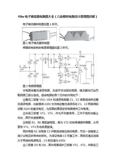
40w电子镇流器电路图大全(六款模拟电路设计原理图详解)电子镇流器实物图如图1所示。
图1 电子镇流器实物图根据实物绘制的电路原理图如图2所示。
图2 电路原理图本电路由整流滤波电路、功率开关与驱动电路、镇流器与灯丝负载回路三部分组成。
组成电路的各个元件的作用如下:①整流二极管VD1~VD4和滤波电容器C1、C2串联组成桥式整流滤波电路,功能是将220V交流电经整流滤波后在C1、C2两端得到空载310V的直流电压,为后面的高频逆变电路提供工作电源。
②功率三极管VT1、VT2,作为开关管使用,工作于饱和与截止状态,其开关速度要快。
③电阻R1、R6是起振电阻,是为VT2初始导通提供偏置,从而激发VT1、VT2形成自激振荡。
同时电阻R1与电容C3并联组成降压启动电路,可在一定程度上减少过电压所带来的损失。
为保证电容C3可靠工作,其耐压值应选择大于两倍的电源电压,C3耐压值为630V.④二极管D5和D6,其作用是保护三极管VT1、VT2,并联在三极管基极和发射极之间可以大大削弱电荷存储效应,从而提高三极管开关速度。
⑤变压器T起信号互感耦合作用。
它是由单股芯线T1、T2、T3绕在磁环上形成的,由于开关管与其驱动电路部分是紧密联系相互依存,因此它们参数之间的关系在生产过程中比较难确定。
此电路中T1为3圈、T2为3圈、T3为5圈。
⑥电容C4并接于VT2基极和发射极之间,可防止基极和发射极间电位突变,能在一定程度上保护三极管VT2.⑦电阻R2、R3、R4、R5为保护电阻,用来保护三极管的,但是作用有限。
⑧电容C5是启动电容,有隔直流通交流的作用,阻止310V的直流电压直接进入日光灯管,允许20kHz的高频交流电压通过。
⑨扼流圈L、谐振电容C6组成串联谐振电路,其作用是起辉日光灯管和限制灯管工作电流。
电子镇流器的基本功能是将50Hz的工频电源转换成20kHz高频电源,而直接点亮日光灯管。
其工作过程是:接通电源后,经整流滤波后的310V直流电压通过C3、R1并联再与R5串联,给VT2的基极提供一个窄电流脉冲使VT2首先导通。

原理图很简单,用555产生一个大约500KHz的脉冲信号(在3脚输出,与555相关的大家问一下度娘就行了,在这里不赘述),频率值大家就自己算了,我测试的时候R1R2都是10KC2用的是104瓷片电容。
8050和8550是为了克服后面场效应管的G极电容而设定的,真正实现(快速开关)的效果。
场效应管可以用IRF630、IRF640,IRF3205、75NF75,80N75等大部分N沟道场效应管,(这个主要看个人所需功率)。
关键部分是线圈和谐振电容的搭配,我实验时是1mm的线径9圈,并联了3个223和两个102电容(22*1000)(10*100)pf,静态电流比较大,达到了260mA左右,功率在5W已下时,VCC取12V左右,线圈20圈,静态电流可以在20mA以下(我试过的,主要看大家调试经验了,呵呵)。
次级线圈n2和c2也很重要,当n2没有与c2并联时,我得出的效果是:次级线圈与初级线圈压紧时,次级感应的电流最大,当松开时(哪怕是很小的距离),电流急剧下降,效率也迅速降低。
有了C2,次级线圈与初级线圈并不是挨得最近的时候电流最大,而是离开一段距离(接近1CM位置)后的一个点(位置),电流最大,效率达到最高(不知道大家能不能调到这一步),这样对大家绕线圈工艺也要求不是很高。
告诉大家个绕好线圈的方法:在一个光滑骨架上先用油纸卷一层,然后在上面整齐地绕线圈(整齐的,不要绕乱),绕好一层后先不要放开(放开是话全散了),用502或其他快速凝固的胶水滴在上面封固,硬化后再接着绕,可以绕出很漂亮的线圈。
(这个方法是我小学时候偶然发现的)。
还要注意的是要注意,线圈工作在很高的频率,容易发生很明显的趋(集)负效应,这个大家可以用多股小线径的铜线并饶。
否则线圈容易发热,我实验时很随意的,实际应用中大家注意。
最后祝大家制作成功(=^ ^=)。

l e d屏专用V A开关电源电原理图公司内部编号:(GOOD-TMMT-MMUT-UUPTY-UUYY-DTTI-l e d屏专用5V40A开关电源,用T L494、K A7500等集成块,通用设计TL494电路图的工作原理,主要是各元件的功能整流器之前的不用说了吧?494 脉宽调制输出至V3、V4。
494 的各脚功能请看其pdf资料。
1 脚是比较器+输入端,接电压监测。
如图,VR1 是输出电压调整。
V3、V4 是功率推动三极管。
T2是推动变压器,将推动电压提高以驱动末级功率管,末级工作在开关状态。
V2、V3 接成推挽功率放大。
VD5、VD6是反峰保护二极管。
R3、C8是尖峰吸收网络。
VD9、VD10、C9 组成全波整流滤波,给494供电。
T1 的右部分就是低压部分了。
整流滤波输出,没什么特别的。
220V交流电经VD1整流,C5,C6滤波得到300V左右直流电。
此电压经R1,R2分压后约150V给C7充电,经T1高压8,9脚绕组,T2绕组8,6脚,V2等形成启动电流。
T2反馈绕组7,9绕组,10,6绕组产生感应电压,使V1,V2轮流导通。
因此在T1低压供电绕组(6,7,13)产生电压,经VD9,VD10整流,C9滤波,给TL494,,V3,V4等供电。
此时输出电压较低。
TL494启动后其8脚,11脚轮流输出脉冲,推动V3,V4,经T2反馈给绕组(7.9,10.6)激励V1,V2。
使V1,V2,由自激状态转入受控状态。
T2输出绕组电压上升,此电压经R31,R29,R30,VR1分压后反馈给TL494的1脚(电压反馈)使输出电压稳定。
J1,J2是电流取样电阻,充电或输出时J1,J2产生压降。
此电压经R36反馈给TL494的15脚(电流反馈)使充电或输出电流恒定。
大体原理已经说清楚了,具体原理还有什么不明白追问,我就不一一说明每个元件的作用了。
R8,R9,R40 是V2的偏置电阻,VD8反馈整流,经R10,R11到V2基极,加速V2导通,C11是加速电容,可以加速V2的导通和截止。

LED驱动电路简介文章出处:转载作者:林继刚俞安琪人气:139发表时间:2010-7-27 15:52:25摘要: LED照明是今年来快速兴起发展的一种新型光源,它的许多良好特点使得它的应用面越来越广。
LED的单向导电特性使人一般认为应该用直流驱动,但是对直流恒压和限流的装置在保证比较好的限流特性时,自身功耗是很大的,所以使系统的效率大为降低。
只有用较高频率的交流来驱动LED,并且用在呈现较大阻抗时自身功耗小的电感或电容来限流,才能把LED驱动电路的限流特性和自身功耗都做得比较理想。
本文分析介绍了几种LED驱动电路,供行业内人士参考。
LED驱动电路除了要满足安全要求外,还应具备另外两个基本功能,一是尽可能保持恒流特性,尤其在电源电压发生±15%的变动时,仍应能保持输出电流在±10%的范围内变动。
二是应保持较低的自身功耗,这样才能使LED 的系统效率保持在较高水平。
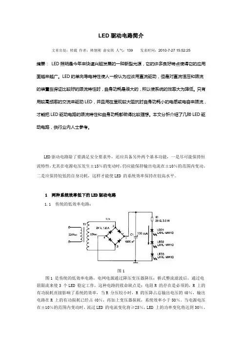
1 两种系统效率低下的LED驱动电路1.1 传统的低效率电路:图1图1 是传统的低效率电路,电网电源通过降压变压器降压;桥式整流滤波后,通过电阻限流来使3 个LED 稳定工作,这种电路的致命缺点是:电阻R 的存在是必须的,R 上的有功损耗直接影响了系统的效率,当R 分压较小时,R 的压降占总输出电压的40%,输出电路在R 上的有功损耗已经占40%,再加上变压器损耗,系统效率小于50%。
当电源电压在±10%的范围内变动时,流过LED 的电流变化将≥25%,LED 上的功率变化将达到30%。
当R 分压较大时,在电源电压在±10%的范围内变动时,虽说能使输出到LED 的功率变化减少,但系统效率将更低。
图21.2采用集成稳压元件的LED驱动电路图2是在图1 的基础上加了一个集成稳压元件MC7809,使输出端的电压基本稳定在9V,限流电阻R 可用得很小也不会因为电源电压的不稳定造成LED 的超载。
但是此电路除了保证LED 的基本恒定输出外,效率还是很低的。

l e d屏专用V A开关电源电原理图The latest revision on November 22, 2020led屏专用5V40A开关电源,用TL494、KA7500等集成块,通用设计TL494电路图的工作原理,主要是各元件的功能整流器之前的不用说了吧494 脉宽调制输出至V3、V4。
494 的各脚功能请看其pdf资料。
1 脚是比较器+输入端,接电压监测。
如图,VR1 是输出电压调整。
V3、V4 是功率推动三极管。
T2是推动变压器,将推动电压提高以驱动末级功率管,末级工作在开关状态。
V2、V3 接成推挽功率放大。
VD5、VD6是反峰保护二极管。
R3、C8是尖峰吸收网络。
VD9、VD10、C9 组成全波整流滤波,给494供电。
T1 的右部分就是低压部分了。
整流滤波输出,没什么特别的。
220V交流电经VD1整流,C5,C6滤波得到300V左右直流电。
此电压经R1,R2分压后约150V给C7充电,经T1高压8,9脚绕组,T2绕组8,6脚,V2等形成启动电流。
T2反馈绕组7,9绕组,10,6绕组产生感应电压,使V1,V2轮流导通。
因此在T1低压供电绕组(6,7,13)产生电压,经VD9,VD10整流,C9滤波,给TL494,,V3,V4等供电。
此时输出电压较低。
TL494启动后其8脚,11脚轮流输出脉冲,推动V3,V4,经T2反馈给绕组(,)激励V1,V2。
使V1,V2,由自激状态转入受控状态。
T2输出绕组电压上升,此电压经R31,R29,R30,VR1分压后反馈给TL494的1脚(电压反馈)使输出电压稳定。
J1,J2是电流取样电阻,充电或输出时J1,J2产生压降。
此电压经R36反馈给TL494的15脚(电流反馈)使充电或输出电流恒定。
大体原理已经说清楚了,具体原理还有什么不明白追问,我就不一一说明每个元件的作用了。
R8,R9,R40 是V2的偏置电阻,VD8反馈整流,经R10,R11到V2基极,加速V2导通,C11是加速电容,可以加速V2的导通和截止。

常用电器原理图与维修雷志远普通耳塞带录音耳塞RR L LRLGR L GR L G普通电风扇原理图调速装置等效电路C 安全装置定时装置调速装置电动机匹配电容BR1D51N4007T 113001T 213001D61N4007R6R5C 1L12-3TL310-15TL22-3TL4荧光台灯电路图R2R3R7R4R9C 3C 4C 5C 6C 2D21N4007D11N4007D41N4007D31N4007灯管B荧光节能台灯原理与维修电子节能灯具有低电压启辉、无频闪、无噪音、高效节能、开灯瞬间即亮、使用寿命长(3000小时以上,为普通白炽灯的3倍多)等优点,很受消费者的欢迎(尤其在电源电压波动频繁的地区)。
电子节能灯有玻罩型和裸露型。
玻罩型又有球型、球柱型、工艺型等三个系列,前两个系列均有全透明、刻花、彩色刻花和乳白色4个品种。
它具有外形美观、安装时不易损坏灯管、耐碰撞等优点;裸露型则有H型、UH型、3U型、4U型、2D型及螺旋型等。
按发光的颜色分,则可分为红、绿、蓝、黄(色温为2700K,属暖色光,类似于白炽灯的光色)、白(色温以6400K居多,属冷色光,类似于日光灯的光色);而色温为5000K的灯管因光色接近于自然光,对眼睛无刺激,更适合于学生和精细工作。
本文介绍的电子节能灯电路见图1,印板图见图2。
该电路已加有软启动(灯丝预热)电路,可延长灯管寿命。
多应用于护目灯和外销灯具中。
【荧光节能台灯原理】对于电路工作原理,分析如下:R1、R5、R6为三极管T2的启动电阻。
电源接通后,T2饱和导通,300V电源经C5、灯丝、变压器L4、L3,三极管T2、T2发射极电阻R6、地,给C5充电。
充电后期,由于有电流流经L3,L1、L2、L3又绕在同一个铁心上,故L2、L1产生感应电压,L2感应电压上负下正,促使T2由饱和进入截止状态,而L1则上正下负,促使T1由截止进入保和导通状态。
T2截止后,T1饱和导通。
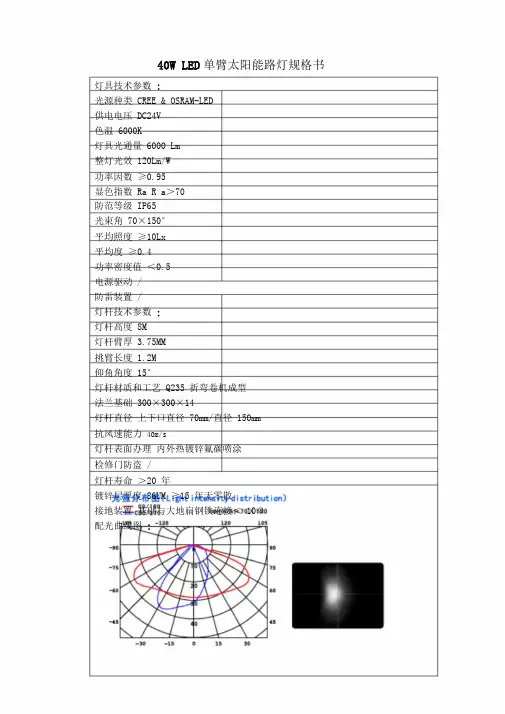
40W LED单臂太阳能路灯规格书灯具技术参数:光源种类 CREE & OSRAM-LED供电电压 DC24V色温 6000K灯具光通量 6000 Lm整灯光效 120Lm/W功率因数≥0.95显色指数 Ra R a>70防范等级 IP65光束角 70×150°平均照度≥10Lx平均度≥0.4功率密度值<0.5电源驱动 /防雷装置 /灯杆技术参数:灯杆高度 8M灯杆臂厚 3.75MM挑臂长度 1.2M仰角角度 15°灯杆材质和工艺 Q235 折弯卷机成型法兰基础 300×300×14灯杆直径上下口直径 70mm/直径 150mm抗风速能力40m/s灯杆表面办理内外热镀锌氟碳喷涂检修门防盗 /灯杆寿命>20 年镀锌层厚度 86UM ≥15 年无零散接地装置基础与大地扁钢铁连接< 10Ω配光曲线图:1.太阳能电池组件参数功率(W) 120规格(mm ) 1200 ×670 ×35 工作电压(V) 17.5数量 1工作电流(A) 6.67A开路电压(V) 21.6短路电流(A) 7.27钢化玻璃厚度( mm ) 3.2钢化玻璃透光率>93%边框资料铝边框表面办理阳极氧化接线盒防范等级 IP65太阳能电池片效率 16.2%组件变换效率 18.4%2.锂蓄电池规格参数额定电压( V) 12容量(Ah) 120数量 1内阻(m Ω) 3.86短路电流(A) 2980自放电≤2%/ 月(25 ℃)端子种类 GFM-24使用温度与寿命的关系曲线不同样放电深度与循环寿命的关系曲线放电容量与温度的关系曲线15.6V15.0V均衡充电电压充电电压与环境温度(电池14.4V表面温度)曲线14.10V13.8V13.83V13.50V13.2V13.23V浮充充电电压12.6V-20 °C -10 °C 0°C 10°C 20°C 30°C 40°C 45°C50°CCharge voltage Vs ambient temperature curve100)% (量容余剩80600°C10° C20° C 40自放电与温度的关系曲线40°C 30° C200 3 6 9 12 15 18 21 24存放时间(月)自放电特点曲线3. 太阳能充放电控制器参数系统电压 12V/24V Auto额定负载电流 10A额定充电电流 10A光伏系统最大输入功率 130W/12V; 260W/24V空载耗费 <10mA太阳能输入电压 < 75V / 150V变换效率≤97%MPPT 追踪效率>99.92%超压保护 16.5V ;×2/24V充电限值电压 15.5V ;×2/24V均衡充电电压 15.2V ;×2/24V (25℃)均衡充电间隔 30 天提升充电电压 14.4V ;×2/24V (25℃)浮充电压 13.8V ;×2/24V (25℃)过放返回电压 12.5V ;×2/24V过放电压 11.0V ;×2/24V提升充电时间 2 小时均衡充电时间 1 小时温度补偿 -4.0mv/ ℃/2V ;超温保护 80℃光控开电压 5V光控关电压 6V光控延时 5min工作温度 -35 ℃~ +65 ℃;防范等级 IP651.内建最大功率追踪算法,能显然提升光伏系统的能量利用效率 ,比传统 PWM 充电效率高15% ~20% 左右。
LED 灯的恒流驱动芯片介绍————————————————————————————————作者:————————————————————————————————日期:LED 灯的恒流驱动芯片介绍http:///data/circuitmore.html1 LED 简介发光二极管( LED) 是一种固态光源,利用半导体中的电子和空穴相结合而发出光子,每种LED 所发出的颜色取决于光子的能量,而光子的能量又因其制造材料而异.同一种材料的发光波长很接近,因此每颗LED 的颜色都很纯正,最常见的一般亮度的LED多是红色和草绿色。
LED 晶粒尺寸小,颜色种类多,使用时排列方式又有很大的灵活性,这是它比一般光源优越的地方;另外,LED 与其他光源相比还具有较高的光效和更高的可靠性,供电的方法也比较简单。
因而LED 特别适合用作显示光源.例如,早期LED主要应用于各种仪表、室内音响、电器面板,或用于资讯和状态显示,如股票看板、活动字幕等。
随着LED 亮度的逐渐增强,LED 也逐渐由室内扩展到户外应用,例如户外广告、交通信号、夜景装饰照明、道路照明等。
目前,LED 大多仍限于上述的特殊照明,其缺点是光束较集中,每流明的成本较高,与一般的照明要求尚有一段距离。
但世界各国特别是美国和日本都把这种固态光源看作最具有发展前景的照明光源,并为研发应用于一般照明的白光LED而投入大量的人力和物力,努力早日使LED 应用于普通照明,我国也为此制定了中长期的研发规划.与一般的半导体PN 结一样,LED 的正向导通压降随导通电流的变化并不大,一般为3. 5V 左右,正向压降约有± 16. 6% 的离散,如表1 所示( 资料来源为Luxeon Star 的技术数据,表2 和图1 也来自该公司的数据),不同颜色的LED 的导通压降也不尽相同.表1 LED 的电特性(电流为350mA、结温Tj = 25℃ 时)表2 LED 的光特性( 电流为350mA、结温Tj = 25℃ 时)各种LED 的发光强度随其发光颜色不同而有所差异,如表2 所列。
一、电子镇流器电原理图二、实用电子镇流器电路:13005*2三、胜光15W电子镇流器电路四、40W日光灯电子镇流器电原理图五、用MJE13005×2的20W日光灯电子镇流器七、32w交流电子镇流器电路上图电路由整流滤波电容、高频振荡电路以及输出负载屯路三部分构成。
交流220V经整流滤波输出约300V直流为振荡电路提供电源。
开机后,电源经R5对C3充电,使Vc3迅速升高,从而使VT2迅速达到饱和导通;此时由于T的反馈作用使VTI截止。
VT2一旦导通,则Vc3下降,流过L2的电流减小,引起L2两端一个上负下正的电压。
据同名端原则,L1得到上正下负的反馈电压,从而使VTI迅速饱和导通,同时T的正反馈作用又使VT2迅速截止,如此周而复始形成振荡方波(R6D6、R3D5起续流作用)。
负载回路由L3、L4、C4构成。
VTI、VT2产生的高频振荡方波由L3加给负载作激励源。
灯管点亮前,由C4、L4等形成很大的谐振电梳流过灯丝,使管内氢气电离,进而使水银变为水银蒸汽,C4两端的高电压又使水银蒸汽形成弧光放电,激发管壁荧光粉发光。
灯管点亮后,C4基本上不起作用,此时L4则起阻流作用。
台灯电子镇流器电路图,也可供参考。
常见故障1.VTl、VT2击穿进而导致D1-D4被击穿,此时将引起电源短路;2.R4偏置损坏;3.振荡电路中L5.L6易损坏;4.负载电路中C4因高压易被击穿。
最后特别说明,目前市场上所见的各种40W、32W节能日光灯以及各种环形灯,均可参考此电路进行分析。
八、荧光灯电子镇流器电路图该荧光灯电子镇流器电路由电源电路、高频振荡器和LC串联输出电路组成。
电路中,电源电路由熔断器FU、电子滤波变压器T1、电容器C1、C2、压敏电阻器RV和整流二极管VD1 - VD4组成;高频振荡器电路由晶体管V1、V2,二极管VD5、V D6、电阻器R1一R6、电容器C3一C5和高频变压器TZ组成;LC串联输出电路由限流电感器L、电容器C6、C7和荧光灯管EL组成。