单片机外文翻译--STC89C52处理芯片
- 格式:docx
- 大小:15.85 KB
- 文档页数:8
AT89S52主要性能·与MCS-51单片机产品兼容·8K字节在系统可编程Flash存储器·1000次擦写周期·全静态操作:0Hz~33Hz·三级加密程序存储器·32个可编程I/O口线·三个16位定时器/计数器·八个中断源·全双工UART串行通道·低功耗空闲和掉电模式·掉电后中断可唤醒·看门狗定时器·双数据指针·掉电标识符功能特性描述AT89S52是一种低功耗、高性能CMOS8位微控制器,具有8K 在系统可编程Flash 存储器。
使用Atmel 公司高密度非易失性存储器技术制造,与工业80C51 产品指令和引脚完全兼容。
片上Flash允许程序存储器在系统可编程,亦适于常规编程器。
在单芯片上,拥有灵巧的8 位CPU 和在系统可编程Flash,使得AT89S52为众多嵌入式控制应用系统提供高灵活、超有效的解决方案。
AT89S52具有以下标准功能:8k字节Flash,256字节RAM,32 位I/O 口线,看门狗定时器,2 个数据指针,三个16 位定时器/计数器,一个6向量2级中断结构,全双工串行口,片内晶振及时钟电路。
另外,AT89S52 可降至0Hz 静态逻辑操作,支持2种软件可选择节电模式。
空闲模式下,CPU停止工作,允许RAM、定时器/计数器、串口、中断继续工作。
掉电保护方式下,RAM内容被保存,振荡器被冻结,单片机一切工作停止,直到下一个中断或硬件复位为止。
引脚结构8 位微控制器8K 字节在系统可编程Flash引脚描述VCC : 电源GND: 地P0 口:P0口是一个8位漏极开路的双向I/O口。
作为输出口,每位能驱动8个TTL逻辑电平。
对P0端口写“1”时,引脚用作高阻抗输入。
当访问外部程序和数据存储器时,P0口也被作为低8位地址/数据复用。
在这种模式下,P0具有内部上拉电阻。
STC89C52单片机介绍STC89C52是一款8位单片机,它是XXX生产的一种基于MCS-51内核的单片机。
单片机是指一个集成在一块芯片上的完整计算机系统,它具有一个完整计算机所需要的大部分部件,如CPU、内存、内部和外部总线系统,还会具有外存和外围设备,如通讯接口、定时器和实时时钟等。
最早的单片机设计理念是通过将大量外围设备和CPU集成在一个芯片中,使计算机系统更小,更容易集成进复杂的控制设备当中。
随着单片机技术的发展,现在最强大的单片机系统甚至可以将声音、图像、网络、复杂的输入输出系统集成在一块芯片上。
单片机最早被用在工业控制领域,是由芯片内仅有CPU的专用处理器发展而来。
早期的单片机都是8位或4位的,其中最成功的是INTEL的8031,因为简单可靠而性能不错获得了很大的好评。
此后在8031上发展出了MCS51系列单片机系统。
基于这一系统的单片机系统直到现在还在广泛使用。
随着工业控制领域要求的提高,开始出现了16位单片机,但因为性价比不理想并未得到很广泛的应用。
90年代后随着消费电子产品大发展,单片机技术得到了巨大的提高。
而传统的8位单片机的性能也得到了飞速提高,处理能力比起80年代提高了数百倍。
目前,高端的32位单片机主频已经超过300MHz,性能直追90年代中期的专用处理器,而普通的型号出厂价格跌落至1美元,最高端的型号也只有10美元。
当代单片机系统已经不再只在裸机环境下开发和使用,大量专用的嵌入式操作系统被广泛应用在全系列的单片机上。
而在作为掌上电脑和手机核心处理的高端单片机甚至可以直接使用专用的Windows和Linux操作系统。
STC89C52是一款性价比高、性能不错的8位单片机,它可以广泛应用于各种控制领域,如家电、电子设备、汽车电子等。
单片机是嵌入式系统中最常用的处理器,因此被广泛应用。
实际上,单片机是世界上数量最多的计算机。
几乎所有现代电子和机械产品都集成了单片机,如手机、电话、计算器、家电、电子玩具、掌上电脑和鼠标等。
at89c52单片机简介中英文对照外文翻译文献中英文资料对照外文翻译A T89C52 Single-chip microprocessor introductionSelection of Single-chip microprocessor1. Development of Single-chip microprocessorThe main component part of Single-chip microprocessor as a result of by such centralize to be living to obtain on the chip,In immediate future middle processor CPU。
Storage RAM immediately﹑memoy read ROM﹑Interrupt system、Timer /'s counter along with I/O's rim electric circuit awaits the main microcomputer section,The lumping is living on the chip。
Although the Single-chip microprocessor r is only a chip,Yet through makes up and the meritorous service be able to on sees,It had haveed the calculating machine system property,calling it for this reason act as Single-chip microprocessor r minisize calculating machine SCMS and abbreviate the Single-chip microprocessor。
中文翻译STC89C52处理芯片电气工程的研究和解决方案中心(ceers)艾哈迈德为吉.波特首要性能:与MCS-51单片机产物兼容、8K字节在系统可编程视频存储器、1000次擦拭周期,全静态操作:0Hz~33Hz、三级加密程序存储器,32个可编程I/O接口线、三个16位定时器(计数器),八个中断源、低功能耗空闲和掉电模式、掉电后间断可唤醒,看门狗定时器、双数值指针,掉电标示符。
关键词:单片机,UART串行通道,掉电标示符等前言可以说,二十世纪跨越了三个“点”的时代,即电气时代,电子时代和现已进入的电脑时代。
不过,这种电脑,通常指的是个人计算机,简称PC机。
还有就是把智能赋予各种机械的单片机(亦称微控制器)。
顾名思义,这种计算机的最小系统只用了一片集成电路,即可进行简单的运算可控制。
因为它体积小,通常都是藏在被控机械的内部里面。
它在整个装置中,起着有如人类头脑的作用,他出了毛病,整个装置就会瘫痪。
现在,单片机的种类和适用领域已经十分广泛,如智能仪表、实施工控、通讯设备、导航系统、家用电器等。
各种产品一旦用上了单片机,就你能起到产品升级换代的功效,常在产品名称前冠以形容词——“智能型”,如智能洗衣机等。
接下来就是关于国产STC89C52单片机的一些基本参数。
功能特性描述:STC89C52单片机是一种低功耗、高性能CMOS8位微控制器,具有8K在系统可编程视频播放存贮器使用高密度非易失性存储器技术制造,与工业80C51 产物指令和引脚完全兼容。
片上反射速度允许程序存储器在系统可编程,也适用于常规的程序编写器。
在其单芯片上,拥有灵敏小巧的八位中央处理器和在线系统可编程反射,这些使用上STC89C52微控制器为众多嵌入式的控制应用系统提供高度矫捷的、更加有用的解决方案。
STC89C52微控制器具有以下的标准功效:8K字节的反射速度,256字节的随机存取储存器,32位I/O串口线,看门狗定时器,2个数值指针,三个16为定时器、计数器,一个6向量2级间断结构,片内晶振及钟表电路。

STC89C52是一种带8K字节闪烁可编程可檫除只读存储器(FPEROM-Flash Programable and Erasable Read Only Memory )的低电压,高性能COMOS8的微处理器,俗称单片机。
该器件采用ATMEL 搞密度非易失存储器制造技术制造,与工业标准的MCS-51指令集和输出管脚相兼容。
单片机总控制电路如下图4—1:图4—1单片机总控制电路1.时钟电路STC89C52部有一个用于构成振荡器的高增益反相放大器,引脚RXD和TXD分别是此放大器的输入端和输出端。
时钟可以由部方式产生或外部方式产生。
部方式的时钟电路如图4—2(a) 所示,在RXD 和TXD引脚上外接定时元件,部振荡器就产生自激振荡。
定时元件通常采用石英晶体和电容组成的并联谐振回路。
晶体振荡频率可以在1.2~12MHz之间选择,电容值在5~30pF之间选择,电容值的大小可对频率起微调的作用。
外部方式的时钟电路如图4—2(b)所示,RXD接地,TXD接外部振荡器。
对外部振荡信号无特殊要求,只要求保证脉冲宽度,一般采用频率低于12MHz的方波信号。
片时钟发生器把振荡频率两分频,产生一个两相时钟P1和P2,供单片机使用。
示,RXD接地,TXD接外部振荡器。
对外部振荡信号无特殊要求,只要求保证脉冲宽度,一般采用频率低于12MHz的方波信号。
片时钟发生器把振荡频率两分频,产生一个两相时钟P1和P2,供单片机使用。
RXD接地,TXD接外部振荡器。
对外部振荡信号无特殊要求,只要求保证脉冲宽度,一般采用频率低于12MHz的方波信号。
片时钟发生器把振荡频率两分频,产生一个两相时钟P1和P2,供单片机使用。
(a)部方式时钟电路(b)外部方式时钟电路图4—2时钟电路2.复位及复位电路(1)复位操作复位是单片机的初始化操作。
其主要功能是把PC初始化为0000H,使单片机从0000H单元开始执行程序。
除了进入系统的正常初始化之外,当由于程序运行出错或操作错误使系统处于死锁状态时,为摆脱困境,也需按复位键重新启动。
STC89C52是一种带8K字节闪烁可编程可檫除只读存储器(FPEROM-Flash Programable and Erasable Read Only Memory )的低电压,高性能COMOS8的微处理器,俗称单片机。
该器件采用ATMEL搞密度非易失存储器制造技术制造,与工业标准的MCS-51指令集和输出管脚相兼容。
单片机总控制电路如下图4—1:图4—1单片机总控制电路1.时钟电路STC89C52内部有一个用于构成振荡器的高增益反相放大器,引脚RXD 和TXD分别是此放大器的输入端和输出端。
时钟可以由内部方式产生或外部方式产生。
内部方式的时钟电路如图4—2(a) 所示,在RXD和TXD引脚上外接定时元件,内部振荡器就产生自激振荡。
定时元件通常采用石英晶体和电容组成的并联谐振回路。
晶体振荡频率可以在1.2~12MHz之间选择,电容值在5~30pF之间选择,电容值的大小可对频率起微调的作用。
外部方式的时钟电路如图4—2(b)所示,RXD接地,TXD接外部振荡器。
对外部振荡信号无特殊要求,只要求保证脉冲宽度,一般采用频率低于12MHz 的方波信号。
片内时钟发生器把振荡频率两分频,产生一个两相时钟P1和P2,供单片机使用。
示,RXD接地,TXD接外部振荡器。
对外部振荡信号无特殊要求,只要求保证脉冲宽度,一般采用频率低于12MHz的方波信号。
片内时钟发生器把振荡频率两分频,产生一个两相时钟P1和P2,供单片机使用。
RXD接地,TXD接外部振荡器。
对外部振荡信号无特殊要求,只要求保证脉冲宽度,一般采用频率低于12MHz的方波信号。
片内时钟发生器把振荡频率两分频,产生一个两相时钟P1和P2,供单片机使用。
(a)内部方式时钟电路(b)外部方式时钟电路图4—2时钟电路2.复位及复位电路(1)复位操作复位是单片机的初始化操作。
其主要功能是把PC初始化为0000H,使单片机从0000H单元开始执行程序。
除了进入系统的正常初始化之外,当由于程序运行出错或操作错误使系统处于死锁状态时,为摆脱困境,也需按复位键重新启动。
海纳电子资讯网:www.fpga-arm.com 为您提供各种IC中文资料 STC89C51RC / RD+ 系列单片机中文指南 ---高可靠 ---超低价 ---低功耗 ---无法解密STC89C51RC,STC89LE51RCSTC89C52RC,STC89LE52RCSTC89C53RC,STC89LE53RCSTC89C54RD+,STC89LE54RD+STC89C58RD+,STC89LE58RD+STC89C516RD+,STC89LE516RD+附录A: 为什么少数用户的普通8051程序烧录后,不能运行附录B: STC89LE516AD,STC89LE516X2附录C: STC89C51RC / RD+ 系列单片机 ISP (DIY)附录D: ISP Demo(演示版)软件(*.hex)及通信协议附录E: 如何实现运行中自定义下载,无仿真器时方便调试附录F: Keil C51高级语言编程的软件如何减少代码长度国内技术支援:宏晶科技(深圳) www.MCU-Memory.com support@dsp-memory.comUpdate date: 2005-2-16 型 号 最高时钟 频 率HzFlash程序存储器RAM数据存储器降低EMI看门狗双倍速P4口ISPIAPEEPROM数据指针串口UART中断源优先级定时器A/D向下兼容Winbond向下兼容Philips向下兼容Atmel 5V 3VSTC89C51 RC0-80M4K512√√√√√√1K+ 21ch+843W78E51P89C51STC89C52 RC0-80M8K512√√√√√√1K+ 21ch+843W78E52P89C52STC89C53 RC0-80M15K512√√√√√√ 21ch+843W78E54P89C54AT89C55STC89C54 RD+0-80M16K1280√√√√√√8K+ 21ch+843W78E54P89C54AT89C55STC89C58 RD+0-80M32K1280√√√√√√8K+ 21ch+843W78E58P89C58AT89C51RCSTC89C516 RD+0-80M63K1280√√√√√√ 21ch+843W78E516P89C51RD2AT89C51RD2STC89LE51 RC0-80M4K512√√√√√√1K+ 21ch+843W78LE51AT89LV51STC89LE52 RC0-80M8K512√√√√√√1K+ 21ch+843W78LE52AT89LV52STC89LE53 RC0-80M14K512√√√√√√ 21ch+843W78LE54AT89LV55STC89LE54 RD+0-80M16K1280√√√√√√8K+ 21ch+843W78LE54AT89LV55STC89LE58 RD+0-80M32K1280√√√√√√8K+ 21ch+843W78LE58AT89LV51RCSTC89LE516RD+0-80M63K1280√√√√√√ 21ch+843W78LE516P89LV51RD2AT89LV51RD2STC89LE516AD0-90M64K512√√√ 21ch+643√需要A/D转换时才选用,8路8位精度在P1.0 - P1.7口,17 个机器周期一次STC89LE516X20-90M64K512√√√√ 21ch+643√ 本应用技术手册是针对有一定8051系列(MCS-51)单片机编程基础的用户编写的。
(文档含英文原文和中文翻译)中英文资料对照外文翻译英文原文:The Description of MCUMCU DescriptionSCM is also known as micro-controller (Microcontroller Unit), commonly used letters of the acronym MCU MCU that it was first used in industrial control. Only a single chip by the CPU chip developed from a dedicated processor. The first design is by a large number of peripherals and CPU on a chip in the computer system, smaller, more easily integrated into a complex and demanding on the volume control device which. INTEL's Z80 is the first designed in accordance with this idea processor, then on the development of microcontroller and dedicated processors have parted ways.Are 8-bit microcontroller early or 4 bits. One of the most successful is the INTEL 8031, for a simple, reliable and good performance was a lot of praise. Then developed in 8031 out of MCS51 MCU Systems. SCM systems based on this system until now is still widely used. With the increased requirements of industrial control field, began a 16-bit microcontroller, because the cost is not satisfactory but have not been very widely used. After 90 years with the great development of consumer electronics, microcontroller technology has been a huge increase. With INTEL i960 series, especially the later series of widely used ARM, 32-bit microcontroller quickly replace high-end 16-bit MCU status and enter the mainstream market. The traditional 8-bit microcontroller performance have been the rapid increase capacity increase compared to 80 the number of times. Currently, high-end 32-bit microcontroller clocked over 300MHz, the performance catching the mid-90's dedicated processor, while the average model prices fall to one U.S. dollars, the most high-end [1] model only 10 dollars. Modern SCM systems are no longer only in the development and use of bare metal environment, a large number of proprietary embedded operating system is widely used in the full range of SCM. The handheld computers and cell phones as the core processing of high-end microcontroller can even use a dedicated Windows and Linux operating systems.SCM is more suitable than the specific processor used in embedded systems, so it was up to the application. In fact the number of SCM is the world's largest computer. Modern human life used in almost every piece of electronic and mechanical products will be integrated single chip. Phone, telephone, calculator, home appliances, electronic toys, handheld computers and computer accessories such as a mouse with a 1-2 in both the Department of SCM. Personal computer will have a large number of SCM in the work. General car with more than 40 SCM, complex industrial control systems may even have hundreds of SCM in the same time work! SCM is not only far exceeds the number of PC and other computing the sum, or even more than the number of human beingsSingle chip, also known as single-chip microcontroller, it is not complete a certain logic chips, but to a computer system integrated into a chip. Equivalent to a micro-computer, and computer than just the lack of a microcontroller I / O devices. General talk: a chip becomes a computer. Its small size, light weight, cheap, for the study, application and development of facilities provided. At the same time, learning to use the MCU is to understand the principle and structure of the computer the best choice.SCM and the computer functions internally with similar modules, such as CPU, memory, parallel bus, the same effect as well, and hard disk memory devices, and different is its performance of these components were relatively weak many of our home computer, but the price is low , usually not more than 10 yuan you can do with it ...... some control for a class is not very complicated electrical work is enough of. We are using automatic drum washing machine, smoke hood, VCD and so on appliances which could see its shadow! ...... It is primarily as a control section of the core componentsIt is an online real-time control computer, control-line is that the scene is needed is a stronger anti-jamming ability, low cost, and this is, and off-line computer (such as home PC), the main difference.Single chipMCU is through running, and can be modified. Through different procedures to achieve different functions, in particular special unique features, this is another device much effort needs to be done, some great efforts are very difficult to do. A not very complex functions if the 50's with the United States developed 74 series, or the 60's CD4000 series of these pure hardware buttoned, then the circuit must be a large PCB board! But if the United States if the 70's with a series of successful SCM market, the result will be a drastic change! Just because you are prepared by microcomputer programs can achieve high intelligence, high efficiency and high reliability!As the microcontroller on the cost-sensitive, so now the dominant software or the lowest level assembly language, which is the lowest level in addition to more than binary machine code language, and as so low why is the use? Many high-level language has reached the level of visual programming Why is not it? The reason is simply that there is no home computer as a single chip CPU, not as hard as a mass storage device. A visualization of small high-level language program which even if only one button, will reach tens of K of size! For the home PC's hard drive in terms of nothing, but in terms of the MCU is not acceptable. SCM in the utilization of hardware resources to be very high for the job so although the original is still in the compilation of a lot of use. The same token, if the giant computer operating system and applications run up to get home PC, home PC, also can not afford to.Can be said that the twentieth century across the three "power" era, that is, the age of electricity, the electronic age and has entered into the computer age. However, this computer, usually refers to the personal computer, referred to as PC. It consists of thehost, keyboard, monitor and other components. Another type of computer, most people do not know how. This computer is to give all kinds of intelligent machines single chip (also known as micro-controller). As the name suggests, this computer system took only a minimal integrated circuit, can be a simple operation and control. Because it is small, usually hidden in the charged mechanical "stomach" in. It is in the device, like the human brain plays a role, it goes wrong, the whole plant was paralyzed. Now, this microcontroller has a very broad field of use, such as smart meters, real-time industrial control, communications equipment, navigation systems, and household appliances. Once all kinds of products were using SCM, can serve to upgrade the effectiveness of products, often in the product name preceded by the adjective - "intelligent," such as intelligent washing machines. Now some technical personnel of factories or other amateur electronics developers to engage in out of certain products, not the circuit is too complicated, that function is too simple and can easily be copied. The reason may be stuck in the product did not use a microcontroller or other programmable logic device.SCM historySCM was born in the late 20th century, 70, experienced SCM, MCU, SoC three stages.First model1.SCM the single chip microcomputer (Single Chip Microcomputer) stage, mainly seeking the best of the best single form of embedded systems architecture. "Innovation model" success, laying the SCM and general computer completely different path of development. In the open road of independent development of embedded systems, Intel Corporation contributed.2.MCU the micro-controller (Micro Controller Unit) stage, the main direction of technology development: expanding to meet the embedded applications, the target system requirements for the various peripheral circuits and interface circuits, highlight the object of intelligent control. It involves the areas associated with the object system, therefore, the development of MCU's responsibility inevitably falls on electrical, electronics manufacturers. From this point of view, Intel faded MCU development has its objective factors. In the development of MCU, the most famous manufacturers as the number of Philips Corporation.Philips company in embedded applications, its great advantage, the MCS-51 single-chip micro-computer from the rapid development of the micro-controller. Therefore, when we look back at the path of development of embedded systems, do notforget Intel and Philips in History.Embedded SystemsEmbedded system microcontroller is an independent development path, the MCU important factor in the development stage, is seeking applications to maximize the solution on the chip; Therefore, the development of dedicated single chip SoC trend of the natural form. As the microelectronics, IC design, EDA tools development, application system based on MCU SoC design have greater development. Therefore, the understanding of the microcontroller chip microcomputer can be, extended to the single-chip micro-controller applications.MCU applicationsSCM now permeate all areas of our lives, which is almost difficult to find traces of the field without SCM. Missile navigation equipment, aircraft, all types of instrument control, computer network communications and data transmission, industrial automation, real-time process control and data processing, extensive use of various smart IC card, civilian luxury car security system, video recorder, camera, fully automatic washing machine control, and program-controlled toys, electronic pet, etc., which are inseparable from the microcontroller. Not to mention the area of robot control, intelligent instruments, medical equipment was. Therefore, the MCU learning, development and application of the large number of computer applications and intelligent control of the scientists, engineers.The single-chip microcomputer AT89S52 MCU as an example, the pair for further description:AT89S52 MCUFeatures• Compatible with MCS-51 Products• 8K Bytes of In-System Programmable (ISP) Flash Memory – Endurance: 10,000 Write/Erase Cycles• 4.0V to 5.5V Operating Range• Fully Static Operation: 0 Hz to 33 MHz• Three-level Program Memory Lock• 256 x 8-bit Internal RAM• 32 Programmable I/O Lines• Three 16-bit Timer/Counters• Eight Interrupt Sources• Full Duplex UART Serial Channel• Low-power Idle and Power-down Modes• Interrupt Recov ery from Power-down Mode• Watchdog Timer • Dual Data Pointer• Power-off Flag • Fast Programming Time• Flexible ISP Programming (Byte and Page Mode)• Green (Pb/Halide-free) Packaging Option1.DescriptionThe AT89S52 is a low-power, high-performance CMOS 8-bit microcontroller with 8K bytes of in-system programmable Flash memory. The device is manufactured using Atmel’s high-density nonvolatile memory technology and is compatible with the indus-try-standard 80C51 instruction set and pinout. The on-chip Flash allows the program memory to be reprogrammed in-system or by a conventional nonvolatile memory pro-grammer. By combining a versatile 8-bit CPU with in-system programmable Flash on a monolithic chip, the Atmel AT89S52 is a powerful microcontroller which provides a highly-flexible and cost-effective solution to many embedded control applications.The AT89S52 provides the following standard features: 8K bytes of Flash, 256 bytes of RAM, 32 I/O lines, Watchdog timer, two data pointers, three 16-bit timer/counters, a six-vector two-level interrupt architecture, a full duplex serial port, on-chip oscillator, and clock circuitry. In addition, the AT89S52 is designed with static logic for operation down to zero frequency and supports two software selectable power saving modes. The Idle Mode stops the CPU while allowing the RAM, timer/counters, serial port, and interrupt system to continue functioning. The Power-down mode saves the RAM con-tents but freezes the oscillator, disabling all other chip functions until the next interrupt or hardware reset.2.Pin DescriptionVCC :Supply voltage.GND :Ground.Port 0:Port 0 is an 8-bit open drain bidirectional I/O port. As an output port, eachpin can sink eight TTL inputs. When 1s are written to port 0 pins, the pins can be used as high-impedance inputs. Port 0 can also be configured to be the multiplexed low-order address/data bus during accesses to external program and data memory. In this mode, P0 has internal pull-ups. Port 0 also receives the code bytes during Flash programming and outputs the code bytes dur-ing program verification. External pull-ups are required during program verification.Port 1:Port 1 is an 8-bit bidirectional I/O port with internal pull-ups. The Port 1 output buffers can sink/source four TTL inputs. When 1s are written to Port 1 pins, they are pulled high by the inter-nal pull-ups and can be used as inputs. As inputs, Port 1 pins that are externally being pulled low will source current (IIL) because of the internal pull-ups. In addition, P1.0 and P1.1 can be configured to be the timer/counter 2 external count input (P1.0/T2) and the timer/counter 2 trigger input (P1.1/T2EX), respectively, as shown in the follow-ing table.Port 1 also receives the low-order address bytes during Flash programming and verification.Port 2:Port 2 is an 8-bit bidirectional I/O port with internal pull-ups. The Port 2 output buffers can sink/source four TTL inputs. When 1s are written to Port 2 pins, they are pulled high by the inter-nal pull-ups and can be used as inputs. As inputs, Port 2 pins that are externally being pulled low will source current (IIL) because of the internal pull-ups. Port 2 emits the high-order address byte during fetches from external program memory and dur-ing accesses to external data memory that use 16-bit addresses (MOVX @ DPTR). In this application, Port 2 uses strong internal pull-ups when emitting 1s. During accesses to external data memory that use 8-bit addresses (MOVX@ RI), Port 2 emits the contents of the P2 Special Function Register. Port 2 also receives the high-order address bits and some control signals during Flash program-ming and verification.Port 3:Port 3 is an 8-bit bidirectional I/O port with internal pull-ups. The Port 3 output buffers can sink/source four TTL inputs. When 1s are written to Port 3 pins, they are pulled high by the inter-nal pull-ups and can be used as inputs. As inputs, Port 3 pins that are externally being pulled low will source current (IIL) because of the pull-ups. Port 3 receives some control signals for Flash programming and verification. Port 3 also serves the functions of various special features of the AT89S52, as shown in the fol-lowing table.RST:Reset input. A high on this pin for two machine cycles while the oscillator is running resets the device. This pin drives high for 98 oscillator periods after the Watchdog times out. The DISRTO bit in SFR AUXR (address 8EH) can be used to disable this feature. In the default state of bit DISRTO, the RESET HIGH out feature is enabled.ALE/PROG:Address Latch Enable (ALE) is an output pulse for latching the low byte of the address during accesses to external memory. This pin is also the program pulse input (PROG) during Flash programming. In normal operation, ALE is emitted at a constant rate of 1/6 the oscillator frequency and may be used for external timing orclocking purposes. Note, however, that one ALE pulse is skipped dur-ing each access to external data memory. If desired, ALE operation can be disabled by setting bit 0 of SFR location 8EH. With the bit set, ALE is active only during a MOVX or MOVC instruction. Otherwise, the pin is weakly pulled high. Setting the ALE-disable bit has no effect if the microcontroller is in external execution mode.PSEN:Program Store Enable (PSEN) is the read strobe to external program memory. When the AT89S52 is executing code from external program memory, PSEN is activated twice each machine cycle, except that two PSEN activations are skipped during each access to exter-nal data memory.EA/VPP:External Access Enable. EA must be strapped to GND in order to enable the device to fetch code from external program memory locations starting at 0000H up to FFFFH. Note, however, that if lock bit 1 is programmed, EA will be internally latched on reset. EA should be strapped to VCC for internal program executions. This pin also receives the 12-volt programming enable voltage (VPP) during Flash programming.XTAL1:Input to the inverting oscillator amplifier and input to the internal clock operating circuit.XTAL2:Output from the inverting oscillator amplifier.3.Memory OrganizationMCS-51 devices have a separate address space for Program and Data Memory. Up to 64K bytes each of external Program and Data Memory can be addressed.3.1 Program MemoryIf the EA pin is connected to GND, all program fetches are directed to external memory. On the AT89S52, if EA is connected to VCC, program fetches to addresses 0000H through 1FFFH are directed to internal memory and fetches to addresses 2000H through FFFFH are to external memory.3.2 Data MemoryThe AT89S52 implements 256 bytes of on-chip RAM. The upper 128 bytes occupy a parallel address space to the Special Function Registers. This means that the upper 128 bytes have the same addresses as the SFR space but are physically separate from SFR space. When an instruction accesses an internal location above address 7FH, the address mode used in the instruction specifies whether the CPU accesses the upper 128bytes of RAM or the SFR space. Instructions which use direct addressing access the SFR space. For example, the following direct addressing instruction accesses the SFR at location 0A0H (which is P2).MOV 0A0H, #dataInstructions that use indirect addressing access the upper 128 bytes of RAM. For example, the following indirect addressing instruction, where R0 contains 0A0H, accesses the data byte at address 0A0H, rather than P2 (whose address is 0A0H).MOV @R0, #dataNote that stack operations are examples of indirect addressing, so the upper 128 bytes of data RAM are available as stack space.4.Watchdog Timer (One-time Enabled with Reset-out)The WDT is intended as a recovery method in situations where the CPU may be subjected to software upsets. The WDT consists of a 14-bit counter and the Watchdog Timer Reset (WDTRST) SFR. The WDT is defaulted to disable from exiting reset. To enable the WDT, a user must write 01EH and 0E1H in sequence to the WDTRST register (SFR location 0A6H). When the WDT is enabled, it will increment every machine cycle while the oscillator is running. The WDT timeout period is dependent on the external clock frequency. There is no way to disable the WDT except through reset (either hardware reset or WDT overflow reset). When WDT over-flows, it will drive an output RESET HIGH pulse at the RST pin.4.1 Using the WDTTo enable the WDT, a user must write 01EH and 0E1H in sequence to the WDTRST register (SFR location 0A6H). When the WDT is enabled, the user needs to service it by writing 01EH and 0E1H to WDTRST to avoid a WDT overflow. The 14-bit counter overflows when it reaches 16383 (3FFFH), and this will reset the device. When the WDT is enabled, it will increment every machine cycle while the oscillator is running. This means the user must reset the WDT at least every 16383 machine cycles. To reset the WDT the user must write 01EH and 0E1H to WDTRST. WDTRST is a write-only register. The WDT counter cannot be read or written. When WDT overflows, it will generate an output RESET pulse at the RST pin. The RESET pulse dura-tion is 98xTOSC, where TOSC = 1/FOSC. To make the best use of the WDT, it should be serviced in those sections of code that will periodically be executed within the time required to prevent a WDT reset.4.2 WDT During Power-down and IdleIn Power-down mode the oscillator stops, which means the WDT also stops. While in Power-down mode, the user does not need to service the WDT. There are two methods of exiting Power-down mode: by a hardware reset or via a level-activated external interrupt which is enabled prior to entering Power-down mode. When Power-down is exited with hardware reset, servicing the WDT should occur as it normally does whenever the AT89S52 is reset. Exiting Power-down with an interrupt is significantly different. The interrupt is held low long enough for the oscillator to stabilize. When the interrupt is brought high, the interrupt is serviced. To prevent the WDT from resetting the device while the interrupt pin is held low, the WDT is not started until the interrupt is pulled high. It is suggested that the WDT be reset during the interrupt service for the interrupt used to exit Power-down mode. To ensure that the WDT does not overflow within a few states of exiting Power-down, it is best to reset the WDT just before entering Power-down mode. Before going into the IDLE mode, the WDIDLE bit in SFR AUXR is used to determine whether the WDT continues to count if enabled. The WDT keeps counting during IDLE (WDIDLE bit = 0) as the default state. To prevent the WDT from resetting the AT89S52 while in IDLE mode, the user should always set up a timer that will periodically exit IDLE, service the WDT, and reenter IDLE mode. With WDIDLE bit enabled, the WDT will stop to count in IDLE mode and resumes the count upon exit from IDLE.5. UARTThe UART in the AT89S52 operates the same way as the UART in the AT89C51 and AT89C52. For further information on the UART operation, please click on the document link below:/dyn/resources/prod_documents/DOC4316.PDF6. Timer 0 and 1Timer 0 and Timer 1 in the AT89S52 operate the same way as Timer 0 and Timer 1 in the AT89C51 and AT89C52. For further information on the timers’ operation, please click on the document link below:/dyn/resources/prod_documents/DOC4316.PDF7. Timer 2Timer 2 is a 16-bit Timer/Counter that can operate as either a timer or an event counter. The type of operation is selected by bit C/T2in the SFR T2CON. Timer 2 has three operating modes: capture, auto-reload (up or down counting), and baud rate generator. The modes are selected by bits in T2CON, as shown in Table 6-1. Timer 2 consists of two 8-bit registers, TH2 and TL2. In the Timer function, the TL2 register is incremented every machine cycle. Since a machine cycle consists of 12 oscillator periods, the count rate is 1/12 of the oscil-lator frequency.In the Counter function, the register is incremented in response to a 1-to-0 transition at its corre-sponding external input pin, T2. In this function, the external input is sampled during S5P2 of every machine cycle. When the samples show a high in one cycle and a low in the next cycle, the count is incremented. The new count value appears in the register during S3P1 of the cycle following the one in which the transition was detected. Since two machine cycles (24 oscillator periods) are required to recognize a 1-to-0 transition, the maximum count rate is 1/24 of the oscillator frequency. To ensure that a given level is sampled at least once before it changes, the level should be held for at least one full machine cycle.7.1 Capture ModeIn the capture mode, two options are selected by bit EXEN2 in T2CON. If EXEN2 = 0, Timer 2 is a 16-bit timer or counter which upon overflow sets bit TF2 in T2CON. This bit can then be used to generate an interrupt. If EXEN2 = 1, Timer 2 performs the same operation, but a 1-to-0 transi-tion at external input T2EX also causes the current value in TH2 and TL2 to be captured into RCAP2H and RCAP2L, respectively. In addition, the transition at T2EX causes bit EXF2 in T2CON to be set. The EXF2 bit, like TF2, can generate an interrupt.7.2 Auto-reload (Up or Down Counter)Timer 2 can be programmed to count up or down when configured in its 16-bit auto-reload mode. This feature is invoked by the DCEN (Down Counter Enable) bit located in the SFR T2MOD . Upon reset, the DCEN bit is set to 0 so that timer 2 will default to count up. When DCEN is set, Timer 2 can count up or down, depending on the value of the T2EX pin. Timer 2 automatically counting up when DCEN = 0. In this mode, two options are selected by bit EXEN2 in T2CON. If EXEN2 = 0, Timer 2 counts up to 0FFFFH and then sets the TF2 bit upon overflow. The overflow also causes the timer registers to be reloaded with the 16-bit value in RCAP2H and RCAP2L. The values in Timer in Capture ModeRCAP2H and RCAP2L are preset by software. If EXEN2 = 1, a 16-bit reload can be triggered either by an overflow or by a 1-to-0 transition at external input T2EX. This transition also sets the EXF2 bit. Both the TF2 and EXF2 bits can generate an interrupt if enabled. Setting the DCEN bit enables Timer 2 to count up or down, as shown in Figure 10-2. In this mode, the T2EX pin controls the direction of the count. A logic 1 at T2EX makes Timer 2 count up. The timer will overflow at 0FFFFH and set the TF2 bit. This overflow also causes the 16-bit value in RCAP2H and RCAP2L to be reloaded into the timer registers, TH2 and TL2, respectively. A logic 0 at T2EX makes Timer 2 count down. The timer underflows when TH2 and TL2 equal the values stored in RCAP2H and RCAP2L. The underflow sets the TF2 bit and causes 0FFFFH to be reloaded into the timer registers. The EXF2 bit toggles whenever Timer 2 overflows or underflows and can be used as a 17th bit of resolution. In this operating mode, EXF2 does not flag an interrupt.8. Baud Rate GeneratorTimer 2 is selected as the baud rate generator by setting TCLK and/or RCLK in T2CON. Note that the baud rates for transmit and receive can be different if Timer 2 is used for the receiver or transmitter and Timer 1 is used for the other function. Setting RCLK and/or TCLK puts Timer 2 into its baud rate generator mode. The baud rate generator mode is similar to the auto-reload mode, in that a rollover in TH2 causes the Timer 2 registers to be reloaded with the 16-bit value in registers RCAP2H and RCAP2L, which are preset by software. The baud rates in Modes 1 and 3 are determined by Timer 2’s overflow rate according to the fol -lowing equation.The Timer can be configured for either timer or counter operation. In most applications, it is con-figured for timer operation (CP/T2 = 0). The timer operation is Timer 2 Overflow Rate Modes 1 and 3 Baud Rates = 16different for Timer 2 when it is used as a baud rate generator. Normally, as a timer, it increments every machine cycle (at 1/12 the oscillator frequency). As a baud rate generator, however, it increments every state time (at 1/2 the oscillator frequency). The baud rate formula is given below.where (RCAP2H, RCAP2L) is the content of RCAP2H and RCAP2L taken as a 16-bit unsigned integer.This figure is valid only if RCLK or TCLK = 1 in T2CON. Note that a rollover in TH2 does not set TF2 and will not generate an inter-rupt. Note too, that if EXEN2 is set, a 1-to-0 transition in T2EX will set EXF2 but will not cause a reload from (RCAP2H, RCAP2L) to (TH2, TL2). Thus, when Timer 2 is in use as a baud rate generator, T2EX can be used as an extra external interrupt. Note that when Timer 2 is running (TR2 = 1) as a timer in the baud rate generator mode, TH2 or TL2 should not be read from or written to. Under these conditions, the Timer is incremented every state time, and the results of a read or write may not be accurate. The RCAP2 registers may be read but should not be written to, because a write might overlap a reload and cause write and/or reload errors. The timer should be turned off (clear TR2) before accessing the Timer 2 or RCAP2 registers.9. Programmable Clock OutA 50% duty cycle clock can be programmed to come out on P1.0. This pin, besides being a regular I/O pin, has two alternate functions. It can be programmed to input the external clock for Timer/Counter 2 or to output a 50% duty cycle clock ranging from 61 Hz to 4 MHz (for a 16-MHz operating frequency). To configure the Timer/Counter 2 as a clock generator, bit C/T2 (T2CON.1) must be cleared and bit T2OE (T2MOD.1) must be set. Bit TR2 (T2CON.2) starts and stops the timer. The clock-out frequency depends on the oscillator frequency and the reload value of Timer 2 capture registers (RCAP2H, RCAP2L), as shown in the following equation.In the clock-out mode, Timer 2 roll-overs will not generate an interrupt. This behavior is similar to when Timer 2 is used as a baud-rate generator. It is possible to use Timer 2 as a baud-rate gen-erator and a clock generator simultaneously. Note, however, Modes 1 and 3Oscillator Frequency Baud Rate 32[65536-RCAP2H,RCAP2L]=⨯Oscilator Frequency Clock-Out Frequency=4[65536-(RCAP2H,RCAP2L)]⨯。
单片机居家安全报警系统外文文献翻译(含:英文原文及中文译文)英文原文Design of Home Safety Alarm System Based on Single Chip MicrocomputerAbstractThis design is to study the field of home safety alarm based on single-chip microcomputer, and design a home safety alarm system that is based on STC89C52 single chip microcomputer and is cost-effective and easy to install. The alarm system adopts the communication mode of wireless communication and GSM communication and the modular design concept. It detects different types of risk factors in the home environment through different types of sensor units, and feedbacks the environmental parameters of different rooms to the main control unit. The control unit makes corresponding decisions and issues alarm instructions when necessary to ensure the safety of the home environment. The system is simple and convenient to operate and has a high degree of intelligence. It can detect home risk factors and prevent dangerous accidents.Keywords: home security alarm system; wireless communication; GSM1 Introduction1.1 Hidden dangers and detection in modern home lifeIn the modern home life, people cannot live without convenient living materials such as running water, electricity, and natural gas. However, they bring convenience to us and also increase the unsafe factors in the home life, leaking water pipes, accidental fires, gas leaks, etc. An accident can bring irreparable damage to the family. With the increasing population of the city and the increasing mobility of the population, the crime rate of theft and house robbery has been high for many years. Traditional anti-theft doors and windows have a certain preventive effect, and there are also many security risks. A wide variety of decoration materials, furniture, and decorative items provide us with convenience and beautify the home while alsocontaminating formaldehyde. Therefore, the safety of the home environment has received increasing attention in recent years. How to create a comfortable, healthy and safe home environment has become a hot topic of common concern. In recent years, electronic technology has been changing with each passing day, and communication technology is flourishing. Among them, the development of chip technology and sensor technology is particularly prominent, which provides new options for the solution of home security issues. The use of a home safety alarm device with a microcontroller and a sensor as its core enables the detection of various risk factors in the home, such as gas concentration, formaldehyde content, leakage of water pipes, and theft of rooms, etc. The system can perform remote alarms in a timely manner and notify the user Solve it.1.2 Selected topics and meaningWith the rapid development of science and technology and economic level, people's requirements for the home environment have evolved from the initial satisfaction of simple housing development to the emphasis on the human needs of residential housing. As a result, many safe, comfortable, fast, and convenient smart communities have emerged. where safety is the primary goal. In addition to human factors, the establishment of security systems is an indispensable and important measure for the realization of smart residential security.At present, there are many types of home security products on the market, which can be roughly divided into several relatively independent categories such as anti-theft alarms, video surveillance, and access control systems. Some products have fewer functions, and products with more comprehensive functions have relatively higher prices. Installation is complicated. In other words, there is an urgent need for a product that requires a price to be popular, strong functions, simple installation, easy use, reliable work, and low false alarm rate. Therefore, starting from the actual application, this article systematically elaborates that the use of the system does not need to change the power lines in the home. It has low cost, does not affect aesthetics, wireless communication, and is easy to use. It is suitable for general househo ld use. Home security is closely related to each of us. The use of home security alarm devicescan improve the quality of life of people and make life more secure and convenient. Because of the advantages of the system and the unmatched price/performance ratio of the 51 series microcontrollers, it will be used in future development. Has a broad market prospects and development potential.1.3 Research Status and Development Trends at Home and AbroadIn recent years, with the rapid development of electronic information technology, computer technology, communication technology and sensor technology, there are more and more products related to home security alarms. Domestic and foreign companies such as Siemens, Honeywell, Bosch, Shenzhen Yingmao and many other companies have developed a series of home security alarm products. They generally have wired or wireless communication functions to complete some alarm functions and have carried out Successful application. For example, Siemens' product portfolio includes general-purpose security and security solutions and services, including access control systems, intrusion detection, video surveillance systems, on-site service control centers, and emergency management systems. Thanks to the installation of the Siemens fire and voice evacuation system, the Jinmao Tower and the Grand Hyatt Shanghai, the world's top hotel, provide safe and comfortable working and living environments for thousands of people. It can be foreseen that the smart residential community will become the development trend of the construction industry in the future, and the home security alarm system will become an integral part of the intelligent residential community. In particular, as people's living standards improve, people using home security alarm system equipment will More and more, people's lives will be more comfortable and safer.2 home security alarm system overall design2.1 Overall Design Scheme of Home Security Alarm SystemThe design of this system is a new home security alarm system that integrates single-chip microcomputer control technology, sensor detection technology, and communication technology. The system is based on the single-chip microcomputer and consists of various detection units placed in different rooms and main control units responsible for decision-making. Each detection unit is responsible for detectingvarious conditions of the indoor environment, such as temperature, humidity, formaldehyde content, leaking water, etc., and then sending the collected data to the main control unit through wireless communication, and the main control unit makes a decision and issues a corresponding The instruction controls the operation of the system, thus realizing the automatic detection and automatic alarm of the indoor environment and maintaining the safety of the indoor environment. The hardware of the system consists of eight parts: main control unit, fire detection unit, water leakage detection unit, anti-theft detection unit, gas leak detection unit, formaldehyde content detection unit, wireless communication module, and GSM network communication module. Ensure the normal operation of the system. The circuit of the system is mainly composed of a power supply module, a microcontroller module, a sensor module, a wireless module, a display module, and an alarm module.2.2 main control unitThe main control unit, as the control center of the system, is responsible for receiving the information of each detection unit through the wireless module, processing the information, finding the alarm information to issue a corresponding alarm, and promptly notifying the user for processing. The main control unit can complete tasks such as GSM network SMS alarm, sound and light alarm, LED screen display, and keyboard control. The GSM short message module is used to send and receive short messages so as to monitor home security. A variety of sensors are used to collect home information, and information fusion technology is used to obtain more reliable alarm information. After receiving the alarm information, the owner responded to the SMS to control and handle the situation on the site, so as to ensure home security and theft prevention. The system is simple in structure, easy to install and debug, and easy to use.DetectorThe detector is used to detect various environmental information in the room. The environmental information is sent to the main control unit so that the main control unit can process the information in time according to the information. The sensor is the core component of the detector. According to the detection situation,sensors of different types and different principles constitute different detectors. The detectors involved in the system mainly include the following types:(1) Fire detectorFire detectors are mainly installed in the kitchen. It uses a combination of smoke sensors and temperature and humidity sensors. Smoke sensors mainly include ion smoke sensors and photoelectric smoke sensors. The system uses ion smoke sensors. The ionized smoke sensor contains an internal radiation source 241. The current and voltage of the ionization chamber inside and outside the sensor are stable under normal conditions. When a fire occurs, the ionization chamber ionizes positive and negative ions under the action of an electric field. The two io ns move toward the positive and negative poles, and the internal current and voltage change to generate an alarm signal. The temperature and humidity sensor can convert the temperature and humidity of the environment into analog signals. These analog signals are converted into digital signals that can be processed by the MCU under the action of their own processing chip. In the event of a fire, the temperature and humidity in the room will rise sharply within a short period of time. Comprehensive temperature and humidity conditions can prevent false alarms due to external interference from the smoke sensor.(2) Water leak detectorThe leak detector is mainly installed in the bathroom. Its working principle is mainly to use the conductive characteristics of water. The two probes of the detector are installed slightly higher than the ground, and are respectively connected to an I/O pin and GND pin of the microcontroller. When water leakage occurs, the water level is higher than the height of the probe. The two probes of the detector are turned on, and the level of the I/O pin of the microcontroller is set low to generate an alarm signal.(3) Theft detectorThe anti-theft detector is installed above the window. The detection part is mainly composed of pyroelectric and infrared sensors. When a gangster enters through the window, pyroelectric and infrared laser sensors can generate alarm signalsat the same time. The combination of the two sensors can prevent false alarms caused by small animals or accidents. An important component of a pyroelectric sensor is a piezoelectric ceramic dielectric that maintains its polarization after being poled, known as spontaneous polarization. Spontaneous polarization decreases with increasing temperature and drops to zero at the Curie point. Therefore, when this material is exposed to infrared radiation and the temperature rises, the surface charge will decrease, which corresponds to the release of a part of the charge and is therefore called pyroelectricity. The released charge can be converted to a voltage output via an amplifier, thereby generating an alarm signal. When radiation continues to act on the pyroelectric element to balance its surface charge, it no longer releases charge. Therefore, pyroelectric sensors cannot detect constant infrared radiation. The infrared detector employs a photoelectric switch. The photoelectric switch (photoelectric sensor) is an abbreviation of the photoelectric proximity switch. It uses the object to block or reflect the light beam and strobes the circuit by a synchronous circuit to detect the presence or absence of an object. The photoelectric switch converts the input current into an optical signal on the transmitter, and the receiver then detects the target object according to the received light intensity or presence or absence.(4) Gas leak detectorThe gas is mainly composed of hydrogen, methane, carbon monoxide, and ethylene, and the natural gas is mainly composed of methane, ethane, propane, and other components. It can be seen that in both gases, methane is an important component of them. By detecting the methane content, it can be determined whether gas or natural gas leaks occur. The methane sensor converts the information related to the methane concentration into analog signals. These analog signals can be converted into digital signals by the A/D chip and sent to the microcontroller. The microcontroller can obtain the indoor methane content according to the size of the digital data. Calculate the concentration of gas and natural gas so that detection and alarm can be achieved.(5) Formaldehyde detectorFormaldehyde is generally considered to be the number one killer of the indoorenvironment. Its release period is generally 3-15 years, and its harm is very serious for the human body, especially infants, pregnant women, the elderly and chronic patients. Formaldehyde mainly exists on the floor, decoration plates, furniture, carpets, paints, and glue. People can easily overlook its existence, but it can cause serious damage to people's health. The formaldehyde sensor uses the electrochemical formaldehyde gas sensor HCHO produced by Dart Sensor. This sensor is developed based on a breath alcohol sensor and is suitable for monitoring in most environments (-20°C~+50°C) (for special applications, it can be used at higher temperatures). This sensor is simple in design, with few components and its cost is reduced. It does not require power supply excitation. It only requires power during signal processing and display, so it is only a simple small battery cell.communication deviceThis system mainly adopts wireless communication methods, which avoids complicated laying of lines and is both beautiful and convenient. The main control unit and each subunit communicate with the wireless module 24L01. The effective range is 60 meters, which fully meets the needs of home use. The communication between the main control unit and the user adopts the GSM (mobile phone network) method. The alarm system can send the information in the home to the user as a short message. The user can also control the running of the home system by sending an SMS.Home Security Alarm System Functions and Working PrinciplesThe main control unit of the system can be placed in the living room, and the detection unit can be installed in different rooms of the house. For example, the fire detection unit is installed in the kitchen, the leak detection unit may be installed in the toilet, the anti-theft alarm detection unit is installed above the door and window, the gas leak detection unit is installed in the kitchen, and the formaldehyde content detection unit is placed in the living room or the bedroom. The detection unit placed in different locations sends information to the main control unit in real time through the wireless device. Once a fire, leaking water pipe, burglary, or gas leak occurs, the main control unit will immediately receive an alarm signal. Then the main control unitThe unit will judge and process the alarm signal, get the alarm type, make an audible and visual alarm, and notify the user through the GSM network. The home security alarm system has six main functions: Mobile phone network intelligent alarm. When an unexpected situation in the home is detected, an alarm is sent through a text message. It can monitor the concentration of gas or natural gas in the home, discover gas leaks, and promptly report an alarm. Anti-theft function, when a thief enters, immediately makes an alarm, and promptly informs the police and the household head; Intelligent fire alarm, immediately when the fire occurs in the home, to alarm, to reduce the loss of property; Intelligent waterproof detection function, found a leak in the home, timely closure of the main valve, And notify the owner by SMS to avoid the loss; The system can be controlled by the remote controller, which is easy to use and easy to operate.3 Hardware Design of Home Security Alarm System3.1 Design of the main control unitThe main controller consists of power supply, GSM communication module, wireless communication module, display device, button, and remote controller. The structure is shown in the figure.Figure 3 main control unit system diagram Power section uses the AC220/DC5V power supply module, after the power supply voltage transformer voltage regulator, and finally get a stable 5V voltage to the microcontroller and other electrical equipment. The display device uses 12864 liquid crystal, 12864 is the abbreviation of dot matrix number of 128*64 dot matrix LCD module, 12864 LCD with Chinese font library can display 4 rows and 8 columns of 32 characters with 16 16 dot matrix, each The display RAM can display 1 Chinese character or 2 16×8 lattice full height ASCII code characters, that is, each display can display up to 32 Chinese characters or 64 ASCII characters. The display of indoor and outdoor temperature, humidity, light intensity, and system working status is realized through the liquid crystal, so that people can understand the working status of the system in real time. The basic circuit for displaying the liquid crystal is shown in Figure 4. Figure 4 LCD connection circuit diagram The GSM mobile network communication module is selected from theSiemens TC35 module, which is a dual-band 900/1800MHz highly integrated GSM module, it is easy to integrate, cost-effective, good product quality and performance The system guarantees that the system communicates with the user's mobile phone via SMS, which is convenient and quick. The GSM module can transmit voice and data signals and connect the SIM card reader and antenna respectively through the interface connector and antenna connector. The automatic baud rate is 1.2kb/s~115kb/s. It supports Short Message Service (SMS) in Text and PDU formats, and can send text messages and make phone calls. The module expansion circuit is shown in Figure 5, and the features are described below. Information transmission content: V oice and data power: Single power supply 3.3V ~ 5.5V Frequency band: Dual-band GSM900MHz and DCS1800MHz (Phase 2+) Transmitting power: 2W (GSM900MHz Class 4) 1W (DCS1800MHz Class 1) 8SIM Card Connection: External Antenna: External antenna connected by antenna connector Talk mode: 300mA (Typ.) Figure 5 TC35 peripheral expansion circuit diagram The wireless communication device uses the 24L01 wireless module, and the maximum operating speed is 2Mbps. It is highly efficient GFSK modulation and has strong anti-interference ability. Up to 126 available channels to meet the needs of multi-point communication and frequency hopping communication, built-in hardware CRC error detection and point-to-multipoint communication address control; Low power consumption 1. 9 - 3. 6V operation, 22uA in standby mode Under power-down mode is 900nA; Built-in 2. 4Ghz antenna, small and exquisite; The module can be set by software address, can be directly used by various microcontrollers, software programming is very convenient. When connecting with P0 port of 51 series single-chip microcomputer, it needs to add 10K pull-up resistor and it is not necessary to connect with other ports. For other series of microcontrollers, if it is 5V, please refer to the output current of the IO of this series of microcontrollers. If it exceeds 10mA, series resistor divider is required. If it is 3. 3V, it can be directly connected to the IO line of the RF2401 module. For example, if A VR series microcontrollers are 5V, they are generally connected in series with 2K resistors. The keypad is used to set the basic parameters of the main control unit. It can also set the parameters through theSAA3010T remote control. The remote control receiver uses HS0038. The connection circuit with the microcontroller is shown in Figure 6. Figure 6 Infrared remote control receiver circuit we use the receiver head, its drive circuit is simple, easy to control the microcontroller. Its operation method is the same as that of an ordinary TV remote controller, and the operation is simple and easy to use.3.2 Design of fire detection unitThe fire alarm unit is composed of a smoke sensor and a temperature and humidity sensor. The increase of the temperature and humidity sensor can enhance the reliability of the alarm and reduce the occurrence of false alarms. The composition of the fire alarm unit is shown in Figure 8. Fig. 8 System diagram of fire detection unit The smoke sensor converts the collected smoke concentration into an analog signal. After the A/D chip, the analog signal is converted into a digital signal and sent to the microcontroller. Temperature and humidity sensor The DH11 can send temperature and humidity in digital form to the microcontroller, so the signal does not have to be processed. The MCU sends the received information to the master control unit through the wireless communication module 24L01. The type of smoke sensor used in the system is MQ-2. The gas sensitive material used by MQ-2 is tin dioxide (SnO2) with low conductivity in clean air, and its sensitivity to smoke is very high.3.3 Design of leak detection unitThe unit's design mainly utilizes the conductive properties of water. There are two detection probes connected to the microcontroller, which are connected to the I/O pin and the GND pin of the microcontroller. When in use, put the two probes above the bathroom floor. When there is water leakage, the toilet will produce water. The two probes of the detector are connected to the stagnant water. The preset high-level I/O pins are set low. , Generate an alarm signal, the microcontroller then sends the alarm signal to the main control unit through the wireless communication module, thus completing the entire alarm process. The specific structure of the alarm unit is shown in Figure 11.3.4 Design of Gas Leak Detection UnitThe gas leak detection unit is mainly composed of a methane content displayliquid crystal, a methane sensor, a wireless communication module, and a buzzer alarm. The structure is shown in FIG. Figure 12 shows the gas leakage detection unit system. Among them, the liquid crystal display is a 5110 liquid crystal display. Its features are: Cost-effective, LCD1602 can display 32 characters, and Nokia5110 can display 15 Chinese characters, 30 characters, Nokia5110 bare screen only 8. 8 yuan, LCD1602 generally about 15 yuan, LCD12864 generally 50 to 70 yuan; interface is simple, only four I / O lines can drive, LCD1602 need 11 I / O lines, LCD12864 need 12 root. The speed is 20 times that of the LCD12864 and 40 times that of the LCD1602. The model selected for the methane sensor is GJ4. Its output is analog and needs to be sent to the microcontroller via A/D conversion. Its use is similar to the smoke sensor.3.5 Design of formaldehyde monitoring unitFormaldehyde detection unit is mainly composed of formaldehyde sensor, operational amplifier, wireless communication module and sound and light alarm. The formaldehyde sensor converts the formaldehyde concentration into electrical signals. The signal is processed by the operational amplifier and then input to the single-chip microcomputer. The single-chip microcomputer judges the signal and sends the formaldehyde content signal to the main control unit through the wireless communication module. The sensor contains a conventional two-electrode fuel cell sensor. The working electrode discharges electrons to the counter electrode through an external circuit and is consumed at the counting electrode end with the reduction of oxygen. The internal circuit is realized by the ion current in the electrolyte. Well-designed to facilitate the growth of electrolyte. The rise and fall of the electrolyte varies with the changes in ambient temperature and humidity, but the normal operation will not affect the calibration value. The specific circuit shown in Figure.3.6 Design of anti-theft alarm unitThe anti-theft alarm unit is a double detector consisting of a pyroelectric sensor and an infrared sensor. Compared with conventional pyroelectric or infrared single sensor systems, Shuangjian detectors have significantly reduced their false alarm rates.When the Shuangjian detector works, the two signals of the pyroelectric sensor and the infrared sensor are processed by the NAND gate and sent to the SCM. When only two sensors respond at the same time, the detector sends an alarm signal to the microcontroller, otherwise no alarm signal is generated. In addition, when designing, Fresnel lens is added to the pyroelectric sensor, and the principle diagram of false alarms that can reduce the external interference signal by changing the lens division method is shown in Fig.16. Fig. 16 System diagram of the anti-theft alarm unit When the double-detection detector works, the pyroelectric sensor and the infrared sensor signal are sent to the single-chip microcomputer after being processed by a NAND gate. When only two sensors respond at the same time, the detector sends an alarm signal to the microcontroller, otherwise no alarm signal is generated. In addition, Fresnel lens is added to the pyroelectric sensor during design. By changing the lens segmentation mode, false alarms due to external interference signals can be reduced. 3.7 Design of Communication SectionThe communication part of this system is mainly composed of GSM mobile network communication module and 24L01 wireless communication module. The GSM module communicates with the user's mobile phone through the mobile phone network of the mobile phone, and the user can understand the security situation at home at any time. Each detection unit communicates with the main control unit through the wireless communication module and feeds back the detected information to the main control unit in time. System Communication Structure Diagram The GSM mobile network communication module uses the TC35 module. Its main features are wide coverage, low cost, reliable quality, and high security. It inherits the standard A T instruction set and RS232 interface standard internally, which makes it easie r for the microcontroller system to control it. It reduces the design of external circuits and simplifies the programming of the program. The hardware circuit is not complicated, but there are many modules used, which increases the complexity of programming and the difficulty of debugging. Therefore, it is necessary to debug each module individually after being debugged by the single chip microcomputer. Communication module application circuit diagram SIM CARD is a mobile communication networkuser identification module. SIM CARD contains the user's user information and is an indispensable tool for communication with mobile phones. There are 6 pins corresponding to each other on the SIM card and the card holder. This is the interface between SIM CARD and TC35. The wireless communication part adopts 24L01 wireless communication module, which has built-in 2. 4Ghz antenna, small size, software address, software programming is very convenient, built-in special voltage regulator circuit, using a variety of power supply including DC/DC switching power supply are very good The communication effect, when connected to the P0 port of the 51 series single-chip microcomputer, requires a pull-up resistor of 10K, and it is not necessary to connect to other ports. The user can set the alarm phone number, alarm mode, work mode, etc. through the keypad. Through the liquid crystal display, you can clearly understand the operating conditions of the system and the environmental parameters in your home, such as temperature, humidity, gas concentration, formaldehyde concentration, leaks, and communication conditions.中文译文基于单片机的居家安全报警系统的设计摘要本设计是对基于单片机的居家安全报警领域进行研究,设计出以STC89C52 单片机为核心的高性价比,易于安装的居家安全报警系统。
中英文对照外文翻译文献(文档含英文原文和中文翻译)翻译:STC89C52处理芯片首要性能:与MCS-51单片机产物兼容、8K字节在系统可编程视频存储器、1000次擦拭周期,全静态操作:0Hz~33Hz、三级加密程序存储器,32个可编程I/O接口线、三个16位定时器(计数器),八个中断源、低功能耗空闲和掉电模式、掉电后间断可唤醒,看门狗定时器、双数值指针,掉电标示符。
关键词:单片机,UART串行通道,掉电标示符等前言可以说,二十世纪跨越了三个“点”的时代,即电气时代,电子时代和现已进入的电脑时代。
不过,这种电脑,通常指的是个人计算机,简称PC机。
还有就是把智能赋予各种机械的单片机(亦称微控制器)。
顾名思义,这种计算机的最小系统只用了一片集成电路,即可进行简单的运算可控制。
因为它体积小,通常都是藏在被控机械的内部里面。
它在整个装置中,起着有如人类头脑的作用,他出了毛病,整个装置就会瘫痪。
现在,单片机的种类和适用领域已经十分广泛,如智能仪表、实施工控、通讯设备、导航系统、家用电器等。
各种产品一旦用上了单片机,就你能起到产品升级换代的功效,常在产品名称前冠以形容词——“智能型”,如智能洗衣机等。
接下来就是关于国产STC89C52单片机的一些基本参数。
功能特性描述:STC89C52单片机是一种低功耗、高性能CMOS8位微控制器,具有8K在系统可编程视频播放存贮器使用高密度非易失性存储器技术制造,与工业80C51 产物指令和引脚完全兼容。
片上反射速度允许程序存储器在系统可编程,也适用于常规的程序编写器。
在其单芯片上,拥有灵敏小巧的八位中央处理器和在线系统可编程反射,这些使用上STC89C52微控制器为众多嵌入式的控制应用系统提供高度矫捷的、更加有用的解决方案。
STC89C52微控制器具有以下的标准功效:8K字节的反射速度,256字节的随机存取储存器,32位I/O串口线,看门狗定时器,2个数值指针,三个16为定时器、计数器,一个6向量2级间断结构,片内晶振及钟表电路。
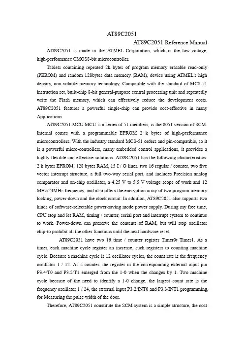
AT89C2051AT89C2051 Reference Manual AT89C2051 is made in the ATMEL Corporation, which is the low-voltage, high-performance CMOS8-bit microcontroller.Tablets containing repeated 2k bytes of program memory erasable read-only (PEROM) and random 128bytes data memory (RAM), device using ATMEL's high density, non-volatile memory technology, Compatible with the standard of MCS-51 instruction set, built-chip 8-bit general-purpose central processing unit and repeatedly write the Flash memory, which can effectively reduce the development costs. AT89C2051 features a powerful single-chip can provide cost-effective in many Applications.AT89C2051 MCU MCU is a series of 51 members, is the 8051 version of SCM. Internal comes with a programmable EPROM 2 k bytes of high-performance microcontrollers. With the industry standard MCS-51 orders and pin-compatible, so it is a powerful micro-controllers, many embedded control applications, it provides a highly flexible and effective solutions. AT89C2051 has the following characteristics: 2 k bytes EPROM, 128 bytes RAM, 15 I / O lines, two 16 regular / counter, two five vector interrupt structure, a full two-way serial port, and includes Precision analog comparator and on-chip oscillator, a 4.25 V to 5.5 V voltage scope of work and 12 MHz/24MHz frequency, and also offers the encryption array of two program memory locking, power-down and the clock circuit. In addition, AT89C2051 also supports two kinds of software-selectable power-saving mode power supply. During my free time, CPU stop and let RAM, timing / counter, serial port and interrupt system to continue to work. Power-down can preserve the contents of RAM, but will stop oscillator chip-to prohibit all the other functions until the next hardware reset.AT89C2051 have two 16 time / counter register Timer0t Timer1. As a timer, each machine cycle register an increase, such registers to counting machine cycle. Because a machine cycle is 12 oscillator cycles, the count rate is the frequency oscillator 1 / 12. As a counter, the register in the corresponding external input pin P3.4/T0 and P3.5/T1 emerged from the 1-0 when the changes by 1. Two machine cycle because of the need to identify a 1-0 change, the largest count rate is the frequency oscillator 1 / 24, the external input P3.2/INT0 and P3.3/INT1 programming, for Measuring the pulse width of the door.Therefore, AT89C2051 constitute the SCM system is a simple structure, the costof the cheapest, most efficient micro-control system, eliminating the external RAM, ROM and interface devices, reducing hardware costs, cost savings, improved The cost-effective system.Clock circuitMCU clock signal used to provide various micro-chip microcontroller operation of the benchmark time, the clock signal is usually used by the form of two circuits: the internal and external shocks oscillation. MCS-51 has a microcontroller internal oscillator for a reverse of the high-gain amplifier, pin XTALl and XTAL2 are here to enlarge the electrical inputs and outputs, as in-house approach, a simple circuit, from the clock Signal relatively stable, and actually used often in this way, as shown in Figure 3-1 in its external crystal oscillator (crystal) or ceramic resonator constituted an internal oscillation, on-chip high-gain amplifier and a reverse Feedback components of the chip quartz crystal or ceramic resonator together to form a self oscillator and generate oscillation clock pulse. Figure 3-1 in the external crystal and capacitors C1 and C2 constitute a parallel resonant circuits, their stability from the oscillation frequency, rapid start-up role, and its value are about 33 PF, crystal frequency of elections 12 MHz.Reset CircuitIn order to initialize the internal MCU some special function register to be reset by the way, will reset after the CPU and system components identified in the initial state, and from the initial state began work properly. MCU is reset on the circuit to achieve, in the normal operation of circumstances, as long as the RST-pin on a two machine cycle time over the high, can cause system reset, but if sustained for the RST-pin HIGH, in a circle on the MCU reset state. After the system will reset input / output (I / 0) home port register for the FFH, stack pointer SP home for 07 H, SBUF built-in value for the indefinite, all the rest of the register-0, the status of internal RAM from the impact of reduction, On the system, when the contents of RAM is volatile. Reset operation There are two situations in which a power-on reset and manual (switch) reduction. The system uses a power-on reset mode. Figure 3-1 in the R0 and C0 formed a power-on reset circuit, and its value for R for 8.2 K, C for the 10 uF.Main features:Compatible the MCS51 command system;Contains the 2KB memory re-programming FLASH (1000);2.7 ~ 6V voltage range;the whole Static work: 0Hz ~ 24KHz;Secrets 2 Program Memory Lock128 × 8-bit internal RAM15 programmable I / O linesTwo 16-bit timer / counter6 interrupt sources, two external interrupt sourcesProgrammable Serial ChannelHigh Precision V oltage Comparator (P1.0,P1.1,P3.6);Have the output port of the LED direct driveLow-power idle and power-down modeThe pin Picture of AT89C2051Picture one the pin of AT89C2051AT89C2051’s functional description:VCC: Power Supply V oltageGND: landP1 port: P1 mouth is a group of 8-bit bi-directional I / O interface, P1.2 ~ P1.7 provide internal pull-up resistor,P1.0 and P1.1 internal supreme pull-up resistor. P1 mouth output buffer can absorb the current 20mA and direct-drive LED.When Programming and calibration, P1 mouth as the eighth address receive.P3 mouth: P3 port P3.0 ~ P3.5, P3.7 is the internal pull-up resistor with the seven bi-directional I / O interface. Did not bring out the P3.6,It as a generic I / O port, but can not visit. Can be used as a fixed-chip input comparator output signal. when P3 write 1, they were highed the internal pull-up resistor can be raised as an input port.P3 port special function as shown in table 1:Table 1 P3 mouth’s special featuresPIN functional characteristics20191817161514131211GND P3.5P3.4P3.3P3.2XTAL1XTAL2P3.1P3.0RST P3.7P1.0P1.1P1.2P1.3P1.4P1.5P1.6P1.7VCC 12345678910RST:Reset output. When the oscillator device reset, RST pin to maintain the high level of two machine cycle time.XTAL1: the RP-oscillator amplifier and internal clock generator input.XTAL2: RP-oscillator output amplifier.TimerOverview of the Timer89C2051 single-chip-chip has two 16-bit timer / counter, That is the timer 0 (T0) and Timer 1 (T1). They all have from time to time and event count function, Can be used for timing control, delay of external events, such as counting and testing occasions. Timer’s T0 and T1—— two 16-bit timers in fact is 16-bit counter plus 1. Among them, T0 compositioned by the two 8-bit special function registers TH0 and TL0; T1 posed by the TH1 and TL1. These functions were controled by the special function registers TMOD and TCONWhen set to the work in the timing, Through the pin count of the external pulse signal. When the input pulse signal generated by the falling edge of 1-0, The value of timer plus 1. At of every machine cycle during the S5P2 sampling pin T0 and T1 the input level, if a machine cycle before sample value of 1, The next machine cycle sampling value is 0, The counter plus 1. Since then during S3P1 of the machine cycle, New value will into the counter.so Detection of a 1-0 transition of the two machine cycles,So The maximum count frequency of oscillation frequency of 1 / 24. In addition to the option of work from time to time or count,Each timer / counter have four kinds of work mode, That is, each of timer circuit kinds of four constitute a structural modelTwo low-power modeIdle modeIn idle mode, CPU to maintain sleep and all-chip peripherals remain active, this way generated in Software, At this point, Chip RAM and all the contents of special function registers remain unchanged. Idle mode was terminated by any interrupt request permission to or hardware reset.P1.0 and P1.1 ,in the non-use of external pull-up resistor on the case should be set to "0", Or in the use of pull-up resistor is set to "1."It should be noted that: when uses of hardware reset Termination idle mode, AT89C2051 is usually stopped from the program until the internal reset control of the two machine cycles before the restore procedure Service. In this case the hardware within the prohibition of the reading and writing of internal RAM, However, to allow access to ports, To eliminate the Hardware reset in the idle mode of port accidents may write, In principle, to enter the idle mode of instruction should not be under the command of a pin or an external memory port for a visit.Power-down modeIn power-down mode, the oscillator to stop working, enter the power-down mode ,Instructions, who was the last one, the implementation of the Directive, Chip RAM and all the contents of special function registers the termination of the previous power-down mode be frozen. To withdraw from power-down mode is the only way to reset the hardware, Reset will redefine all the Special Function Registers but Does not change the contents of RAM before the the Vcc work returned to normal levels Shall be null and void and must be reset to maintain a certain period of time in order to restart and oscillator stabilityP1.0 and P1.1 in the non-use of external pull-up resistor on the case should be set to "0", Or in the use of pull-up resistor is set to "1."OscillatorOscillator connected clientXTAL1: RP-oscillator amplifier and internal clock generator inputXTAL2: RP-oscillator amplifier outputCharacteristics of OscillatorXTAL1, XTAL2 ware the RP-chip oscillator amplifier inputs and outputs, Quartzcrystal can be composed of the clock oscillator or ceramic oscillator, For more information from the external input clock driver AT89C2051, XTAL1 input clock signal from, XTAL2 should be left vacant.As the input to the internal circuit is a 2-flip-flop, Therefore, the external clock signal input without special requirements, However, it must comply with the maximum level and minimum norms and timing中文翻译:AT89C2051AT89C2051数据参考手册AT89C2051是美国ATMEL公司生产的低电压、高性能CMOS8位单片机,片内含2k bytes的可反复擦写的只读程序存储器(PEROM)和128bytes的随机数据存储器(RAM),器件采用ATMEL公司的高密度、非易失性存储技术生产,兼容标准MCS-51指令系统,片内置通用8位中央处理器和可反复擦写的Flash存储器,可有效地降低开发成本。
AT89S52Features•Compatible with MCS-51Products•8K Bytes of In-System Programmable(ISP)Flash Memory–Endurance:10,000 Write/Erase Cycles•4.0V to5.5V Operating Range•Fully Static Operation:0Hz to33MHz•Three-level Program Memory Lock•256x8-bit Internal RAM•32Programmable I/O Lines•Three16-bit Timer/Counters•Eight Interrupt Sources•Full Duplex UART Serial Channel•Low-power Idle and Power-down Modes•Interrupt Recovery from Power-down Mode•Watchdog Timer•Dual Data Pointer•Power-off Flag•Fast Programming Time•Flexible ISP Programming(Byte and Page Mode)•Green(Pb/Halide-free)Packaging Option1.DescriptionThe AT89S52is a low-power,high-performance CMOS8-bit microcontroller with8K bytes of in-system programmable Flash memory.The device is manufactured using Atmel’s high-density nonvolatile memory technology and is compatible with the indus-try-standard80C51instruction set and pinout.The on-chip Flash allows the program memory to be reprogrammed in-system or by a conventional nonvolatile memory pro-grammer.By combining a versatile8-bit CPU with in-system programmable Flash on a monolithic chip,the Atmel AT89S52is a powerful microcontroller which provides a highly-flexible and cost-effective solution to many embedded control applications.The AT89S52provides the following standard features:8K bytes of Flash, 256bytes of RAM,32I/O lines,Watchdog timer,two data pointers,three16-bit timer/counters,a six-vector two-level interrupt architecture,a full duplex serial port, on-chip oscillator,and clock circuitry.In addition,the AT89S52is designed with static logic for operation down to zero frequency and supports two software selectablepower saving modes.The Idle Mode stops the CPU while allowing the RAM, timer/counters,serial port,and interrupt system to continue functioning.The Power-down mode saves the RAM con-tents but freezes the oscillator,disabling all other chip functions until the next interrupt or hardware reset.2.Pin Description2.1VCC:Supply voltage.2.2GND:Ground.2.3Port0:Port0is an8-bit open drain bidirectional I/O port.As an output port, each pin can sink eight TTL inputs.When1s are written to port0pins,the pins can be used as high-impedance inputs.Port0can also be configured to be the multiplexed low-order address/data bus during accesses to external program and data memory.In this mode,P0has internal pull-ups.Port0also receives the code bytes during Flash programming and outputs the code bytes dur-ing program verification.External pull-ups are required during program verification.2.4Port1:Port1is an8-bit bidirectional I/O port with internal pull-ups.The Port1 output buffers can sink/source four TTL inputs.When1s are written to Port1pins, they are pulled high by the inter-nal pull-ups and can be used as inputs.As inputs, Port1pins that are externally being pulled low will source current(IIL)because of the internal pull-ups.In addition,P1.0and P1.1can be configured to be the timer/counter2external count input(P1.0/T2)and the timer/counter2trigger input (P1.1/T2EX),respectively,as shown in the follow-ing table.Port1also receives the low-order address bytes during Flash programming and verification.Port Pin Alternate FunctionsP1.0T2(external count input to Timer/Counter2),clock-outP1.1T2EX(Timer/Counter2capture/reload trigger and directioncontrol)P1.5MOSI(used for In-System Programming)P1.6MISO(used for In-System Programming)P1.7SCK(used for In-System Programming)2.5Port2:Port2is an8-bit bidirectional I/O port with internal pull-ups.The Port2output buffers can sink/source four TTL inputs.When1s are written to Port2pins, they are pulled high by the inter-nal pull-ups and can be used as inputs.As inputs, Port2pins that are externally being pulled low will source current(I IL)because of the internal pull-ups.Port2emits the high-order address byte during fetches from external program memory and dur-ing accesses to external data memory that use 16-bit addresses(MOVX@DPTR).In this application,Port2uses strong internal pull-ups when emitting1s.During accesses to external data memory that use8-bit addresses(MOVX@RI),Port2emits the contents of the P2Special Function Register.Port2also receives the high-order address bits and some control signals during Flash program-ming and verification.2.6Port3:Port3is an8-bit bidirectional I/O port with internal pull-ups.The Port3 output buffers can sink/source four TTL inputs.When1s are written to Port3pins, they are pulled high by the inter-nal pull-ups and can be used as inputs.As inputs, Port3pins that are externally being pulled low will source current(IIL)because of the pull-ups.Port3receives some control signals for Flash programming and verification.Port3also serves the functions of various special features of the AT89S52,as shown in the fol-lowing table.Port Pin Alternate FunctionsP3.0RXD(serial input port)P3.1TXD(serial output port)P3.2INT0(external interrupt0)P3.3INT1(external interrupt1)P3.4T0(timer0external input)P3.5T1(timer1external input)P3.6WR(external data memory write strobe)P3.7RD(external data memory read strobe)2.7RST:Reset input.A high on this pin for two machine cycles while the oscillator is running resets the device.This pin drives high for98oscillator periods after the Watchdog times out.The DISRTO bit in SFR AUXR(address8EH)can be used to disable this feature.In the default state of bit DISRTO,the RESET HIGH out feature is enabled.2.8ALE/PROG:Address Latch Enable(ALE)is an output pulse for latching the lowbyte of the address during accesses to external memory.This pin is also the program pulse input(PROG)during Flash programming.In normal operation,ALE is emitted at a constant rate of1/6the oscillator frequency and may be used for external timing or clocking purposes.Note,however,that one ALE pulse is skipped dur-ing each access to external data memory.If desired,ALE operation can be disabled by setting bit0of SFR location8EH.With the bit set,ALE is active only during a MOVX or MOVC instruction.Otherwise,the pin is weakly pulled high.Setting the ALE-disable bit has no effect if the microcontroller is in external execution mode.2.9PSEN:Program Store Enable(PSEN)is the read strobe to external program memory.When the AT89S52is executing code from external program memory, PSEN is activated twice each machine cycle,except that two PSEN activations are skipped during each access to exter-nal data memory.2.10EA/VPP:External Access Enable.EA must be strapped to GND in order to enable the device to fetch code from external program memory locations starting at 0000H up to FFFFH.Note,however,that if lock bit1is programmed,EA will be internally latched on reset.EA should be strapped to VCC for internal program executions.This pin also receives the12-volt programming enable voltage(VPP) during Flash programming.2.11XTAL1:Input to the inverting oscillator amplifier and input to the internal clock operating circuit.2.12XTAL2:Output from the inverting oscillator amplifier.3.Memory OrganizationMCS-51devices have a separate address space for Program and Data Memory. Up to64K bytes each of external Program and Data Memory can be addressed.3.1Program MemoryIf the EA pin is connected to GND,all program fetches are directed to external memory.On the AT89S52,if EA is connected to VCC,program fetches to addresses 0000H through1FFFH are directed to internal memory and fetches to addresses 2000H through FFFFH are to external memory.3.2Data MemoryThe AT89S52implements256bytes of on-chip RAM.The upper128bytes occupy a parallel address space to the Special Function Registers.This means that the upper128bytes have the same addresses as the SFR space but are physically separate from SFR space.When an instruction accesses an internal location above address7FH,the address mode used in the instruction specifies whether the CPU accesses the upper 128bytes of RAM or the SFR space.Instructions which use direct addressing access the SFR space.For example,the following direct addressing instruction accesses the SFR at location0A0H(which is P2).MOV0A0H,#dataInstructions that use indirect addressing access the upper128bytes of RAM.For example,the following indirect addressing instruction,where R0contains0A0H, accesses the data byte at address0A0H,rather than P2(whose address is0A0H).MOV@R0,#dataNote that stack operations are examples of indirect addressing,so the upper128 bytes of data RAM are available as stack space.4.Watchdog Timer(One-time Enabled with Reset-out)The WDT is intended as a recovery method in situations where the CPU may be subjected to software upsets.The WDT consists of a14-bit counter and the Watchdog Timer Reset(WDTRST)SFR.The WDT is defaulted to disable from exiting reset.To enable the WDT,a user must write01EH and0E1H in sequence to the WDTRST register(SFR location0A6H).When the WDT is enabled,it will increment every machine cycle while the oscillator is running.The WDT timeout period is dependent on the external clock frequency.There is no way to disable the WDT except through reset(either hardware reset or WDT overflow reset).When WDT over-flows,it will drive an output RESET HIGH pulse at the RST pin.4.1Using the WDTTo enable the WDT,a user must write01EH and0E1H in sequence to the WDTRST register(SFR location0A6H).When the WDT is enabled,the user needs to service it by writing01EH and0E1H to WDTRST to avoid a WDT overflow.The 14-bit counter overflows when it reaches16383(3FFFH),and this will reset the device.When the WDT is enabled,it will increment every machine cycle while the oscillator is running.This means the user must reset the WDT at least every16383 machine cycles.To reset the WDT the user must write01EH and0E1H to WDTRST. WDTRST is a write-only register.The WDT counter cannot be read or written.When WDT overflows,it will generate an output RESET pulse at the RST pin.The RESET pulse dura-tion is98xTOSC,where TOSC=1/FOSC.To make the best use of the WDT,it should be serviced in those sections of code that will periodically be executed within the time required to prevent a WDT reset.4.2WDT During Power-down and IdleIn Power-down mode the oscillator stops,which means the WDT also stops. While in Power-down mode,the user does not need to service the WDT.There are two methods of exiting Power-down mode:by a hardware reset or via a level-activated external interrupt which is enabled prior to entering Power-down mode. When Power-down is exited with hardware reset,servicing the WDT should occur as it normally does whenever the AT89S52is reset.Exiting Power-down with an interrupt is significantly different.The interrupt is held low long enough for the oscillator to stabilize.When the interrupt is brought high,the interrupt is serviced.To prevent the WDT from resetting the device while the interrupt pin is held low,the WDT is not started until the interrupt is pulled high.It is suggested that the WDT be reset during the interrupt service for the interrupt used to exit Power-down mode.To ensure that the WDT does not overflow within a few states of exiting Power-down,it is best to reset the WDT just before entering Power-down mode.Before going into the IDLE mode,the WDIDLE bit in SFR AUXR is used to determine whether the WDT continues to count if enabled.The WDT keeps counting during IDLE(WDIDLE bit= 0)as the default state.To prevent the WDT from resetting the AT89S52while in IDLE mode,the user should always set up a timer that will periodically exit IDLE,service the WDT,and reenter IDLE mode.With WDIDLE bit enabled,the WDT will stop to count in IDLE mode and resumes the count upon exit from IDLE.5.UARTThe UART in the AT89S52operates the same way as the UART in the AT89C51 and AT89C52.For further information on the UART operation,please click on the document link below:6.Timer0and1Timer0and Timer1in the AT89S52operate the same way as Timer0and Timer 1in the AT89C51and AT89C52.For further information on the timers’operation, please click on the document link below:7.Timer2Timer2is a16-bit Timer/Counter that can operate as either a timer or an event counter.The type of operation is selected by bit C/T2in the SFR T2CON.Timer2 has three operating modes:capture,auto-reload(up or down counting),and baud rate generator.The modes are selected by bits in T2CON,as shown in Table6-1.Timer2 consists of two8-bit registers,TH2and TL2.In the Timer function,the TL2register isincremented every machine cycle.Since a machine cycle consists of12oscillator periods,the count rate is1/12of the oscil-lator frequency.Table6-1.Timer2Operating ModesRCLK+TCLK CP/RL2TR2MODE00116-bit Auto-reload 01116-bit Capture1X1Baud Rate Generator X X0(Off) In the Counter function,the register is incremented in response to a1-to-0 transition at its corre-sponding external input pin,T2.In this function,the external input is sampled during S5P2of every machine cycle.When the samples show a high in one cycle and a low in the next cycle,the count is incremented.The new count value appears in the register during S3P1of the cycle following the one in which the transition was detected.Since two machine cycles(24oscillator periods)are required to recognize a1-to-0transition,the maximum count rate is1/24of the oscillator frequency.To ensure that a given level is sampled at least once before it changes,the level should be held for at least one full machine cycle.7.1Capture ModeIn the capture mode,two options are selected by bit EXEN2in T2CON.If EXEN2=0,Timer2is a16-bit timer or counter which upon overflow sets bit TF2in T2CON.This bit can then be used to generate an interrupt.If EXEN2=1,Timer2 performs the same operation,but a1-to-0transi-tion at external input T2EX also causes the current value in TH2and TL2to be captured into RCAP2H and RCAP2L, respectively.In addition,the transition at T2EX causes bit EXF2in T2CON to be set. The EXF2bit,like TF2,can generate an interrupt.7.2Auto-reload(Up or Down Counter)Timer2can be programmed to count up or down when configured in its16-bit auto-reload mode.This feature is invoked by the DCEN(Down Counter Enable)bit located in the SFR T2MOD.Upon reset,the DCEN bit is set to0so that timer2will default to count up.When DCEN is set,Timer2can count up or down,depending on the value of the T2EX pin.Timer2automatically counting up when DCEN=0.In this mode,two options are selected by bit EXEN2in T2CON.If EXEN2=0,Timer2 counts up to0FFFFH and then sets the TF2bit upon overflow.The overflow also causes the timer registers to be reloaded with the16-bit value in RCAP2H andRCAP2L.The values in Timer in Capture ModeRCAP2H and RCAP2L are preset by software.If EXEN2=1,a 16-bit reload can be triggered either by an overflow or by a 1-to-0transition at external input T2EX.This transition also sets the EXF2bit.Both the TF2and EXF2bits can generate an interrupt if enabled.Setting the DCEN bit enables Timer 2to count up or down,as shown in Figure 10-2.In this mode,the T2EX pin controls the direction of the count.A logic 1at T2EX makes Timer 2count up.The timer will overflow at 0FFFFH and set the TF2bit.This overflow also causes the 16-bit value in RCAP2H and RCAP2L to be reloaded into the timer registers,TH2and TL2,respectively.A logic 0at T2EX makes Timer 2count down.The timer underflows when TH2and TL2equal the values stored in RCAP2H and RCAP2L.The underflow sets the TF2bit and causes 0FFFFH to be reloaded into the timer registers.The EXF2bit toggles whenever Timer 2overflows or underflows and can be used as a 17th bit of resolution.In this operating mode,EXF2does not flag an interrupt.8.Baud Rate GeneratorTimer 2is selected as the baud rate generator by setting TCLK and/or RCLK in T2CON.Note that the baud rates for transmit and receive can be different if Timer 2is used for the receiver or transmitter and Timer 1is used for the other function.Setting RCLK and/or TCLK puts Timer 2into its baud rate generator mode.The baud rate generator mode is similar to the auto-reload mode,in that a rollover in TH2causes the Timer 2registers to be reloaded with the 16-bit value in registers RCAP2H and RCAP2L,which are preset by software.The baud rates in Modes 1and 3are determined by Timer 2’s overflow rate according to the fol-lowing equation.The Timer can be configured for either timer or counter operation.In most applications,it is con-figured for timer operation (CP/T2=0).The timer operation is different for Timer 2when it is used as a baud rate generator.Normally,as a timer,it increments every machine cycle (at 1/12the oscillator frequency).As a baud rate generator,however,it increments every state time (at 1/2the oscillator frequency).The baud rate formula is given below.Timer 2 Overflow RateModes 1 and 3 Baud Rates = 16Modes 1 and 3Oscillator Frequency Baud Rate 32[65536-RCAP2H,RCAP2L]=×where (RCAP2H,RCAP2L)is the content of RCAP2H and RCAP2L taken as a 16-bit unsigned integer.This figure is valid only if RCLK or TCLK =1in T2CON.Note that a rollover in TH2does not set TF2and will not generate an inter-rupt.Note too,that if EXEN2is set,a 1-to-0transition in T2EX will set EXF2but will not cause a reload from (RCAP2H,RCAP2L)to (TH2,TL2).Thus,when Timer 2is in use as a baud rate generator,T2EX can be used as an extra external interrupt.Note that when Timer 2is running (TR2=1)as a timer in the baud rate generator mode,TH2or TL2should not be read from or written to.Under these conditions,the Timer is incremented every state time,and the results of a read or write may not be accurate.The RCAP2registers may be read but should not be written to,because a write might overlap a reload and cause write and/or reload errors.The timer should be turned off (clear TR2)before accessing the Timer 2or RCAP2registers.9.Programmable Clock OutA 50%duty cycle clock can be programmed to come out on P1.0.This pin,besides being a regular I/O pin,has two alternate functions.It can be programmed to input the external clock for Timer/Counter 2or to output a 50%duty cycle clock ranging from 61Hz to 4MHz (for a 16-MHz operating frequency).To configure the Timer/Counter 2as a clock generator,bit C/T2(T2CON.1)must be cleared and bit T2OE (T2MOD.1)must be set.Bit TR2(T2CON.2)starts and stops the timer.The clock-out frequency depends on the oscillator frequency and the reload value of Timer 2capture registers (RCAP2H,RCAP2L),as shown in the following equation.In the clock-out mode,Timer 2roll-overs will not generate an interrupt.This behavior is similar to when Timer 2is used as a baud-rate generator.It is possible to use Timer 2as a baud-rate gen-erator and a clock generator simultaneously.Note,however,that the baud-rate and clock-out frequencies cannot be determined independently from one another since they both use RCAP2H and RCAP2L.10.InterruptsThe AT89S52has a total of six interrupt vectors:two external interrupts (INT0and INT1),three timer interrupts (Timers 0,1,and 2),and the serial port interrupt.Each of these interrupt sources can be individually enabled or disabled by setting or clearing a bit in Special Function Register IE.IE also contains a global disable bit,EA,Oscilator Frequency Clock-Out Frequency=4[65536-(RCAP2H,RCAP2L)]×which disables all interrupts at once.Note that bit position IE.6is unimplemented. User software should not write a1to this bit position,since it may be used in future AT89products.Timer2interrupt is generated by the logical OR of bits TF2and EXF2in register T2CON.Nei-ther of these flags is cleared by hardware when the service routine is vectored to.In fact,the service routine may have to determine whether it was TF2or EXF2that generated the interrupt,and that bit will have to be cleared in software.The Timer0and Timer1flags,TF0and TF1,are set at S5P2of the cycle in which the timers overflow.The values are then polled by the circuitry in the next cycle.However,the Timer2flag,TF2,is set at S2P2and is polled in the same cycle in which the timer overflows.11.Oscillator CharacteristicsXTAL1and XTAL2are the input and output,respectively,of an inverting amplifier that can be configured for use as an on-chip oscillator.Either a quartz crystal or ceramic resonator may be used.To drive the device from an external clock source, XTAL2should be left unconnected while XTAL1is driven,.There are no requirements on the duty cycle of the external clock signal,since the input to the internal clock-ing circuitry is through a divide-by-two flip-flop,but minimum and maximum voltage high and low time specifications must be observed.12.Idle ModeIn idle mode,the CPU puts itself to sleep while all the on-chip peripherals remain active.The mode is invoked by software.The content of the on-chip RAM and all the special functions regis-ters remain unchanged during this mode.The idle mode can be terminated by any enabled interrupt or by a hardware reset.Note that when idle mode is terminated by a hardware reset,the device normally resumes pro-gram execution from where it left off,up to two machine cycles before the internal reset algorithm takes control.On-chip hardware inhibits access to internal RAM in this event,but access to the port pins is not inhibited.To eliminate the possibility of an unexpected write to a port pin when idle mode is terminated by a reset,the instruction following the one that invokes idle mode should not write to a port pin or to external memory.13.Power-down ModeIn the Power-down mode,the oscillator is stopped,and the instruction that invokes Power-down is the last instruction executed.The on-chip RAM and Special Function Registers retain their values until the Power-down mode is terminated.Exitfrom Power-down mode can be initiated either by a hardware reset or by an enabled external interrupt.Reset redefines the SFRs but does not change the on-chip RAM. The reset should not be activated before VCC is restored to its normal operating level and must be held active long enough to allow the oscillator to restart and stabilize.Article Source;/view/d06e2f95dd88d0d233d46a83.html(截图呢?)。
外文原文AT89S52DescriptionThe AT89s52 is a low-power, high-performance CMOS 8-bit microcomputer with 8K bytes of Flash programmable and erasable read only memory(PEROM). The device is manufactured using Atmel’s high-density nonvolatile memory technology and is compatible with the industry-standard 80C51 and 80C52 instruction set and pinout. The on-chip Flash allows the program memory to be reprogrammed in-system or by a conventional nonvolatile memory programmer. By combining a versatile 8-bit CPU with Flash on a monolithic chip, the Atmel AT89s52 is a powerful microcomputer which provides a highly-flexible and cost-effective solution to many embedded control applications.Pin Configurations: The AT89s52 provides the following standard features: 8K bytes of Flash, 256 bytes of RAM, 32 I/O lines, three 16-bittimer/counters, a six-vector two-level interrupt architecture, a full-duplex serial port, on-chip oscillator, and clock circuitry. In addition, the AT89s52 is designed with static logic for operation down to zero frequency and supports two software selectable power saving modes. The Idle Mode stops the CPU while allowing the RAM, timer/counters, serial port, and interrupt system to continue functioning. The Power-down mode saves the RAM contents but freezes the oscillator, disabling all other chip functions until the next hardware reset.Pin Description·VCC: Supply voltage.·GND: Ground.·Port 0: Port 0 is an 8-bit open drain bi-directional I/O port. As an output port, each pin can sink eight TTL inputs. When 1s are written to port 0 pins, the pins can be used as highimpedance inputs.Port 0 can also be configured to be the multiplexed loworder address/data bus during accesses to external program and data memory. In this mode, P0 has internalpullups.Port 0 also receives the code bytes during Flash programming and outputs the code bytes during program verification. External pullups are required during program verification.·Port 1: Port 1 is an 8-bit bi-directional I/O port with internal pullups. The Port 1 output buffers can sink/source four TTL inputs. When 1s are written to Port 1 pins, they are pulled high by the internal pullups and can be used as inputs. As inputs, Port 1 pins)because of the internal that are externally being pulled low will source current (IILpullups.In addition, P1.0 and P1.1 can be configured to be the timer/counter 2 external count input(P1.0/T2) and the timer/counter 2 trigger input (P1.1/T2EX), respectively, as shown in the following table.Port 1 also receives the low-order address bytes during Flash programming and verification.Port Pin Alternate FunctionP1.0 T2(external count input to Timer/Counter2),clock-outP1.1 T2EX(Time/Counter2 capture/reload triggerand direction control)·Port 2: Port 2 is an 8-bit bi-directional I/O port with internal pullups. The Port 2 output buffers can sink/source four TTL inputs. When 1s are written to Port 2 pins, they are pulled high by the internal pullups and can be used as inputs. As inputs, Port 2 pins)because of the internal that are externally being pulled low will source current (IILpullups.Port 2 emits the high-order address byte during fetches from external program memory and during accesses to external data memory that use 16-bit addresses (MOVX @DPTR). In this application, Port 2 uses strong internal pullups when emitting 1s. During accesses to external data memory that use 8-bit addresses (MOVX @ RI), Port 2 emits the contents of the P2 Special Function Register.Port 2 also receives the high-order address bits and some control signals duringFlash programming and verification.·Port 3: Port 3 is an 8-bit bi-directional I/O port with internal pullups. The Port 3 output buffers can sink/source four TTL inputs. When 1s are written to Port 3 pins, they are pulled high by the internal pullups and can be used as inputs. As inputs, Port 3 pins that are externally being pulled low will source current (I) because of the pullups.ILPort 3 also serves the functions of various special features of the AT89C51, as shown in the following table.Port 3 also receives some control signals for Flash programming and verification.Port Pin Alternate FunctionP3.0 RXD (serial input port)P3.1 TXD(serial output port)P3.2 external interrupt 0P3.3 external interrupt 1P3.4 T0(timer 0 external input)P3.5 T1(timer 1 external input)P3.6 external data memory write strobeP3.7 external data memory read strobe ·RST: Reset input. A high on this pin for two machine cycles while the oscillator is running resets the device.·ALE/PROG: Address Latch Enable is an output pulse for latching the low byte of the address during accesses to external memory. This pin is also the program pulse input (PROG) during Flash programming.In normal operation, ALE is emitted at a constant rate of 1/6 the oscillator frequency and may be used for external timing or clocking purposes. Note, however, that one ALE pulse is skipped during each access to external data memory.If desired, ALE operation can be disabled by setting bit 0 of SFR location 8EH. With the bit set, ALE is active only during a MOVX or MOVC instruction. Otherwise, the pin is weakly pulled high. Setting the ALE-disable bit has no effect if the microcontroller is in external execution mode.·PSEN: Program Store Enable is the read strobe to external program memory.When the AT89s52 is executing code from external program memory, PSEN is activated twice each machine cycle, except that two PSEN activations are skipped during each access to external data memory.·EA/VPP: External Access Enable. EA must be strapped to GND in order to enable the device to fetch code from external program memory locations starting at 0000H up to FFFFH.Note, however, that if lock bit 1 is programmed, EA will be internally latched on reset.EA should be strapped to V CC for internal program executions.This pin also receives the 12-volt programming enable voltage (V PP) during Flash programming when 12-volt programming is selected.·XTAL1I: nput to the inverting oscillator amplifier and input to the internal clock operating circuit.·XTAL2: Output from the inverting oscillator amplifier.Oscillator Characteristics: XTAL1 and XTAL2 are the input and output, respectively, of an inverting amplifier which can be configured for use as an on-chip oscillator, as shown in Figure 1. Either a quartz crystal or ceramic resonator may be used. To drive the device from an external clock source, XTAL2 should be left unconnected while XTAL1 is driven as shown in Figure 2. There are no requirements on the duty cycle of the external clock signal, since the input to the internal clocking circuitry is through a divide-by-two flip-flop, but minimum and maximum voltage high and low time specifications must be observed.Idle Mode: In idle mode, the CPU puts itself to sleep while all the onchip peripherals remain active. The mode is invoked by software. The content of the on-chip RAM and all the special functions registers remain unchanged during this mode. The idle mode can be terminated by any enabled interrupt or by a hardware reset.It should be noted that when idle is terminated by a hard ware reset, the device normally resumes program execution, from where it left off, up to two machine cycles before the internal reset algorithm takes control. On-chip hardware inhibits access tointernal RAM in this event, but access to the port pins is not inhibited. To eliminate the possibility of an unexpected write to a port pin when Idle is terminated by reset, the instruction following the one that invokes Idle should not be one that writes to a port pin or to external memory.Status of External Pins During Idle and Power Down Modes:Power Down Mode: In the power down mode the oscillator is stopped, and the instruction that invokes power down is the last instruction executed. The on-chip RAM and Special Function Registers retain their values until the power down mode is terminated. The only exit from power down is a hardware reset. Reset redefines the SFRs but does not change the on-chip RAM. The reset should not be activated before VCC is restored to its normal operating level and must be held active long enough to allow the oscillator to restart and stabilize.Program Memory Lock Bits: On the chip are three lock bits which can be left unprogrammed (U) or can be programmed (P) to obtain the additional features listed in the table below:Lock Bit Protection ModesWhen lock bit 1 is programmed, the logic level at the EA pin is sampled and latched during reset. If the device is powered up without a reset, the latch initializes to a random value, and holds that value until reset is activated. It is necessary that the latched value of EA be in agreement with the current logic level at that pin in order for the device to function properly.Programming the Flash: The at89s52 is normally shipped with the on-chip Flash memory array in the erased state (that is, contents = FFH) and ready to be programmed. The programming interface accepts either a high-voltage (12-volt) or a low-voltage(VCC) program enable signal.The low voltage programming mode provides a convenient way to program the at89s52 inside the user’s system, while the high-voltage programming mode is compatible with conventional third party Flash or EPROM programmers.The at89s52 is shipped with either the high-voltage or low-voltage programming mode enabled. The respective top-side marking and device signature codes are listed in the following table.The at89s52 code memory array is programmed byte-bybyte in either programming mode. To program any nonblank byte in the on-chip Flash Programmable and Erasable Read Only Memory, the entire memory must be erased using the Chip Erase Mode.Programming Algorithm: Before programming the at89s52, the address, data and control signals should be set up according to the Flash programming mode table and Figures 3 and 4. To program the at89s52, take the following steps.1. Input the desired memory location on the address lines.2. Input the appropriate data byte on the data lines.3. Activate the correct combination of control signals.4. Raise EA/VPP to 12V for the high-voltage programming mode.5. Pulse ALE/PROG once to program a byte in the Flash array or the lock bits. The byte-write cycle is self-timed and typically takes no more than 1.5 ms. Repeat steps 1 through 5, changing the address and data for the entire array or until the end of the object file is reached.Data Polling: The at89s52 features Data Polling to indicate the end of a write cycle. During a write cycle, an attempted read of the last byte written will result in the complement of the written datum on PO.7. Once the write cycle has been completed, true data are valid on all outputs, and the next cycle may begin. Data Polling may begin any time after a write cycle has been initiated.Ready/Busy: The progress of byte programming can also be monitored by the RDY/BSY output signal. P3.4 is pulled low after ALE goes high during programming to indicate BUSY. P3.4 is pulled high again when programming is done to indicate READY.Program Verify: If lock bits LB1 and LB2 have not been programmed, the programmed code data can be read back via the address and data lines for verification. The lock bits cannot be verified directly. Verification of the lock bits is achieved by observing that their features are enabled.Chip Erase:The entire Flash Programmable and Erasable Read Only Memory array is erased electrically by using the proper combination of control signals and by holding ALE/PROG low for 10 ms. The code array is written with all “1”s. The chip erase operation must be executed before the code memory can be re-programmed.Reading the Signature Bytes: The signature bytes are read by the same procedure as a normal verification of locations 030H, 031H, and 032H, except that P3.6 and P3.7 must be pulled to a logic low. The values returned are as follows.(030H) = 1EH indicates manufactured by Atmel(031H) = 51H indicates 89C51(032H) = FFH indicates 12V programming(032H) = 05H indicates 5V programmingProgramming Interface: Every code byte in the Flash array can be written and the entire array can be erased by using the appropriate combination of control signals. The write operation cycle is selftimed and once initiated, will automatically time itself to completion.中文翻译AT89S52AT89s52是美国ATMEL公司生产的低功耗,高性能COMS 8位单片机,片内含8K bytes的可反复擦写的Flash只读程序存储器和256 bytes的随机存取数据存储器(RAM),器件采用ATMEL公司的高密度、非易是失性存储技术生产,与标准MCS-51指令系统及8052产品引脚兼容,片内置通用8位中央处理器(CPU)和Flash存储单元,功能强大AT89s52单片机适用许多较为复杂控制应用场合。
中文4800字附录3:外文翻译AT89C52 monolithic integrated circuit introduction AT89C52 is the low voltage which American ATMEL Corporation produces, the high performance CMOS 8 monolithic integrated circuits, internal may repeatedly scratch read-only program memory (PEROM) and 256bytes random access data-carrier storage (RAM) including 8k bytes which writes, the component uses ATMEL Corporation the high density, the non-volatility memory technology production, is compatible with the standard MCS-51 command system and 8052 product pins, internal sets at general 8 central processor (CPU) and the Flash memory cell, the function formidable AT89C52 monolithic integrated circuit suits in many comparatively plurality of controls application situation.Main performance parameter:Are completely compatible with the MCS-51 product instruction and the pinThe 8k byte may again scratch writes Flash to dodge the fast memory1000 times scratches the write cycleEntire static operation: 0Hz—24MHzThree level of encryption program memory256×8 In byte RAM32 programmable I/O mouth line3 16 fixed time/counters8 interrupt sourcesProgrammable serial UART channelThe low power loss idle and falls the electricity patternFunction characteristic outline:Below AT89C52 provides the standard function: 8k byte Flash dodges the fast memory, 256 byte internal RAM,32 I/O mouth line, 3 16 fixed time/counters, 6 vector two level of interrupt structures, A full-duplex serial passes unguardedly, internal oscillator and clock electric circuit.At the same time, AT89C52 may fall to the 0HZ static state logical operation, and supports the electricity saving working pattern which two kind of softwares may elect.The idle way stops CPU the work, but permits RAM, fixed time/the counter, serial passes unguardedly and the interruption system continues to work.Falls the electricity way to preserve in RAM the content, but the oscillator knock off and forbids other all part work to reposition until the next hardware.The pin function showsVcc: Supply voltageGND: GroundingP0 mouth: The P0 mouth is one group of 8 leaks leads the way extremely the bidirectional I/O mouth, also is the address/data bus multiplying mouth.As outlet with when, each potential energy absorption current way actuates 8 TTL logic gate, when writes “1” to port P0, may take the high impedance input end uses.When visits exterior data-carrier storage or the program memory, when this group of mouth line segment transforms the address (low 8) and the data bus multiplying, pulls the resistance in the visit activation interior.When Flash programming, P0 mouth receive instruction byte, but when program check, when output order byte, verification, outside the request joins pulls the resistanceP1 mouth: P1 is in a belt interior pulls the resistance 8 bidirectional I/O mouth, the P1 output buffer may actuate (absorption or output current) 4 TTL logic gate.Writes “1” to the port, pulls the resistance through internal on to pull the port tothe high level, this time may make the input port.When makes the input port use, because in internal existence pulls the resistance, some pin is pulled lowly by exterior signal when can output electric current (IIL).With at89C51 similarity is, P1.0 and P1.1 also may take separately fixed time/the counter 2 exterior countings inputs (P1.0/T2) and inputs (P1.1/T2EX), see also table 1.Flash programming and program check period, P1 receives the low 8 bit address.P2 mouth: P2 is one has in the interior to pull the resistance 8 bidirectional I/O mouth, the P2 output buffer may actuate (absorption or output current) 4 TTL logic gate.Writes “1” to port P2, pulls the resistance through internal on to pull the port to the high level, this time may make the input port, when makes the input port use, because in internal existence pulls the resistance, some pin is pulled lowly by exterior signal when can output electric current (IIL).When visits exterior program memory or 16 bit address exterior data-carrier storage (e.g. carries out the MOVX@DPTR instruction), the P2 mouth sends out the high 8 bit address data.When visits 8 bit addresses exterior data-carrier storage (for example carries out the MOVX@RI instruction), the P2 mouth outputs the P2 latch the contentWhen Flash programming or verification, P2 also receives the top digit address and some control signal.P3 mouth: The P3 mouth is a group has in the interior to pull the resistance 8 bidirectional I/O mouth.The P3 mouth output buffer may actuate (absorption or output current) 4 TTL logic gate.Reads in “1” when to the P3 mouth, they the position resistance are pulled by the interior in Gao Bingke the achievement to input the port.This time, will be pulled by the outside the low P3 mouth to use to pull resistance output current (IIL).The P3 mouth besides took the general I/O mouth line, a more important use isIn addition, the P3 mouth also receives some to use in Flash dodging the fast memory programming and the program check control signal.RST: Replacement input.When the oscillator works, the RST pin will appear above two machine cycles the high level to cause the monolithic replacement.ALE/PROG: When visits exterior program memory or the data-carrier storage, ALE (address lock saves permission) to output the pulse to use in the lock saving the address the low 8 bytes.In ordinary circumstances, ALE still by clock oscilation frequency 1/6 output fixed pulse signal, therefore it may the foreign output clock or uses in fixed time the goal.Must pay attention: When visits exterior data-carrier storage will jump over a ALE pulse.To Flash memory programming period, this pin also uses in inputting programming pulse (PROG).If has the necessity, may through to in special function register (SFR) area 8EH the unit D0 position position, be possible to forbid the ALE operation.After this position position, only then MOVX and the MOVC instruction can activate ALE.In addition, this pin can pull weakly high, when the monolithic integrated circuit carries out exterior procedure, should establish the ALE prohibition position to be invalid PSEN: The procedure storage permits the (PSEN) output is exterior program memory reads the gating signal, when AT89C52 takes the instruction by exterior program memory (or data), each machine cycle two PSEN is effective, namely outputs two pulses.When visits exterior data-carrier storage, will jump over two RSEN signals.EA/VPP: Exterior visit permission.Wants to cause CPU only to visit exterior program memory (address is 0000H-FFFFH), the EA end must maintain the low level (earth).Must pay attention: If adds mil LB1 to program, when replacement the interiorcan lock saves the EA end condition.If the EA end (meets the Vcc end) for the high level, CPU carries out in the internal procedure memory instruction.When the Flash memory programs, this pin adds on 12V programming permission power source VPP, certainly this must be this component is uses 12V to program voltage VPP.XTAL1: Oscillator inverting amplifier and internal clock generator input end.XTAL2: Oscillator inverting amplifier out-port. Special function register:In at89C52 internal memory, the 80H-FFH altogether 128 units for special function register (SFE), SFR address basement reflection as shown in Table 2.All addresses all are defined by no means, only then a part is defined from the 80H-FFH altogether 128 bytes, but also has quite a part not to define.To the definition unit read-write will not have been Yuan Xiao, the read-out value will be indefinite, but will read in the data will also lose.Should not “1” not read in the data the definition unit, then will possibly entrust with the new function in these units in the future product, in this case, after replacement these unit value always “0”.AT89C52 besides with AT89C51 all fixed time/counters 0 and fixed time/counter 1, but also increased a fixed time/counter 2.Fixed time/the counter 2 control statusbyte is located T2CON、T2MOD (to see Table 4), the register to (RCA02H, RCAP2L) is the timer 2/automatic loads the register again under 16 capture ways or 16 automatic heavy loading way capture.Interrupt register:AT89C52 has 6 interrupt sources, 2 interrupt priorities, the IE register controls each interrupt position, in the IP register 6 interrupt source each may decide as 2 superiordata-carrier storages:AT89C52 has 256 byte internal RAM,80H-FFH high 128 bytes and the special function register (SFR) address is overlap, also is high 128 byte RAM and the special function register address is same, but in physics they are separated.When an instruction visits the 7FH above dummy home address unit, in the instruction uses the addressing way is different, also is the addressing way decision is visits high 128 byte RAM to visit the special function register.If the instruction is the direct addressing way for the visit special function register.For example, following direct addressing instruction visit special function register 0A0H (i.e. P2 mouth) address unit.MOV 0A0H,#dataThe indirect addressing instruction visits high 128 byte RAM, for example, in following indirect addressing instruction, the R0 content is 0A0H, then the visit data byte address is 0A0H, but is not the P2 mouth (0A0H).MOV the @R0,#datastorehouse operation also is the indirect addressing way, therefore, high 128 bit data RAM also may take the storehouse area use.Timer 0 and timer 1:The AT89C52 timer 0 and the timer 1 working and AT89C51 are same.Timer 2:The timer 2 is 16 fixed time/counters.It already may when timer use, also may take the external event counter use, its working chooses by the special function register T2CON C/T2 position.The timer 2 has three workings: The capture way, the automatic heavy loading (upward or downward counting) the way and the baudrate generator way, the working chooses by the T2CON control position, see also table 4.The timer 2 is composed by two 8 register TH2 and TL2, in the timer working, each machine cycle TL2 register value adds 1, because a machine cycle vibrates the clock constitution by 12, therefore, counting speed for oscilation frequency 1/12.When counting working, when on the T2 pin exterior input signal produces by 1 to 0 drops along, the register value adds 1, under this working, each machine cycle 5SP2 period, carries on the sampling to exterior input. If picks in the first machine cycle the value is 1, but the value which picks in the next machine cycle is 0, then is following close on the next cyclical S3P1 period register adds 1.Because distinguishes 1 to need 2 machine cycles to 0 jumps (24 durations of oscillation), therefore, highest counting speed for oscilation frequency 1/24. In order to guarantee the sampling the accuracy, the request input level maintains at least before the change for a complete cyclical the time, guarantees the input signal at least by sampling one time.Capture way:Under the capture way, chooses two ways through T2CON control position EXEN2.If EXEN2=0, the timer 2 is 16 timers or the counter, when counting overflow, to the T2CON overflow symbolized TF2 sets at the position, simultaneously activates the interrupt.If looks up EXEN2=1, the timer 2 completes the same operation, But when the T2EX pin exterior input signal has 1 to 0 negative jumps, also appears in TH2 and the TL2 value is caught separately to in RCAP2H and RCAP2L.Moreover, the T2EX pin signal jump causes in T2CON EXF2 to set at the position, is similar with TF2, EXF2 also can interrupt exactly.Capture way as shown in Figure 4.Automatic heavy loading (upward or downward counter) way:When timer 2 work in 16 automatic heavy loading ways, can to its programming for upward or the downward counting way, this function may (see Table 5) through special function register T2CON the DCEN position (permission downward counting) choose.When replacement, the DCEN position “0”, the timer 2 defaults establishes as the upward counting. When DCEN sets at the position, the timer 2 already may count upwardly also may the downward counting, this is decided by the T2EX pin value,see also Figure 5, when DCEN=0, the timer 2 automatic setups for the upward counting, under this way, in the T2CON EXEN2 control position have two kind of choices, if EXEN2=0, the timer 2 for the upward counting to the 0FFFFH overflow, sets at the position TF2 activation interrupt, simultaneously 16 counter register RCAP2H and the RCAP2L heavy loading, RCAP2H and the RCAP2L value may by the software initialization.When DCEN sets at the position, the timer 2 already may count upwardly also may the downward counting, this is decided by the T2EX pin value, see also Figure 5, when DCEN=0, the timer 2 automatic setups for the upward counting, under this way, in the T2CON EXEN2 control position have two kind of choices, if EXEN2=0, the timer 2 for the upward counting to the 0FFFFH overflow, sets at the position TF2 activation interrupt, simultaneously 16 counter register RCAP2H and the RCAP2L heavy loading, RCAP2H and the RCAP2L value may by the software initialization.Baudrate generator:When T2CON (Table 3) TCLK and RCLK set at the position, fixed time/the counter 2 takes the baudrate generator use.If fixed time/the counter 2 took thetransmitter or the receiver, its transmission and the receive baudrate may be different, the timer 1 uses in other functions, as shown in Figure 7.If RCLK and TCLK set at the position, then timer 2 work in baudrate generator way.The baudrate generator way and the automatic heavy loading way are similar, under this way, the TH2 turn over causes the timer 2 registers is important the new loading with in RCAP2H and the RCAP2L 16 figures, this value establishes by the software.In the way 1 and the way in 3, the baudrate determined by the timer 2 overflow speeds according to the equation below that,Way 1 and 3 baudrate = timer overflow rate /16The timer already can work in fixed time the way also can work in the counting way, in the majority applications, is the work in fixed time the way (C/T2=0).The timer 2 took when baudrate generator, with as the timer operation is different, when usual achievement timer, (1/12 oscilation frequency) checks the value in each machine cycle to add 1, but took when baudrate generator use, (1/2 oscilation frequency) the register value adds 1 in each condition time. The baudrate formula is as follows:The way 1 and 3 baudrate = oscilation frequency/{32×[65536-(RCAP2H, RCAP2L)]}in the formula (RCAP2H, RCAP2L) is in RCAP2H and RCAP2L 16 does not have the sign digit.The timer 2 took the baudrate generator use electric circuit as shown in Figure 7.In when T2CON RCLK or TCLK=1, the baudrate working only then is effective. In the baudrate generator working, the TH2 turn over cannot cause TF2 to set at theposition, therefore does not have the interrupt.But if EXEN2 sets at the position, also the T2EX end produces by 1 to 0 negative jumps, then can cause EXF2 to set at the position, this time cannot load (RCAP2H, RCAP2L) content in TH2 and TL2.Therefore, when the timer 2 takes the baudrate generator use, T2EX may use as the additional exterior interrupt source.Needs to pay attention, when timer 2 work in baudrate, when moves (TR2=1) as the timer, cannot visit TH2 and TL2.Because this time each condition time timer can add 1, to its read-write will obtain a indefinite value.But however, may read to RCAP2 cannot write, because the write operation will be the reload, the write operation possibly command writes with/or the heavy loading makes a mistake.In visits timer 2 or in front of the RCAP2 register, should (eliminate the timer closure TR2).The programmable clock outputs:The timer 2 may output a dutyfactor through the programming from P1.0 is 50% clock signal, as shown in Figure 8.The P1.0 pin besides is a standard I/O mouth, but also may cause it through the programming to take fixed time/the counter 2 exterior clock inputs and the output dutyfactor 50% clock pulse.When the clock oscilation frequency is 16MHz, outputs the clock frequency range is 61Hz-4MHz.When establishes fixed time/the counter 2 as the clock generator, C/T2(T2CON.1)=0, T2OE(T2MOD.1)=1, must or stops the timer by TR2(T2CON.2) start.The clock output frequency is decided in the oscilation frequency and the timer 2 catches the register (RCAP2H, RCAP2L) reload value, the formula is as follows:The output clock frequency = oscillator frequency/{4×[65536-(RCAP2H, RCAP2L)]}under the clock output way, the timer 2 turn over cannot have the interrupt, this characteristic with took when baudrate generator use is similar.When the timer 2 takes the baudrate generator use, Also may take the clock generator use, but needs to pay attention is the baudrate and the clock output frequency cannot separate the determination, this is because they with use RCAP2H and RCAP2L.AT89C52单片机的介绍AT89C52是美国ATMEL公司生产的低电压,高性能CMOS 8位单片机,片内含8k bytes的可反复擦写的只读程序存储器(PEROM)和256bytes的随机存取数据存储器(RAM),器件采用ATMEL公司的高密度、非易失性存储技术生产,与标准MCS-51指令系统及8052产品引脚兼容,片内置通用8位中央处理器(CPU)和Flash存储单元,功能强大AT89C52单片机适合于许多较为复杂控制应用场合。
附录B:外文文献及译文STC89C52 Date SheetDescriptionThe STC89C52 is a low-power,high-performance CMOS 8-bit microcontroller with 8Kbytes of in-system programmable Flash memory. The device is manufactured using Atmel’s high-density nonvolatile memory technology and is compatible with the industry-standard 80C51 instruction set and pinout. The on-chip Flash allows the program memory to be reprogrammed in-system or by a conventional nonvolatile memory programmer. By combining a versatile 8-bit CPU with in-system programmable Flash on a monolithic chip,the Atmel STC89C52 is a powerful microcontroller which provides a highly-flexible and cost-effective solution to many embedded control applications.The STC89C52 provides the following standard features: 8K bytes of Flash,256 bytes of RAM,32 I/O lines,Watchdog timer,two data pointers,three 16-bit timer/counters,a six-vector two-level interrupt architecture,a full duplex serial port,on-chip oscillator,and clock circuitry. In addition,the STC89C52 is designed with static logic for operation down to zero frequency and supports two software selectable power saving modes. The Idle Mode stops the CPU while allowing the RAM,timer/counters,serial port,and interrupt system to continue functioning. The Power-down mode saves the RAM contents but freezes the oscillator,disabling all other chip functions until the next interrupt or hardware reset.VCCSupply voltage.GNDGround.Port 0Port 0 is an 8-bit open drain bidirectional I/O port. As an output port,each pin can sink eight TTL inputs. When 1sare written to port 0 pins,the pins can be used as highimpe dance inputs. Port 0 can also be configured to be the multiplexed loworder address/data bus during accesses to external program and data memory. In this mode,P0 has internal pullups. Port 0 also receives the code bytes during Flash programming and outputs the code bytes during program verification. External pullups are required during program verification.Port 1Port 1 is an 8-bit bidirectional I/O port with internal pullups. The Port 1 output buffers can sink/source four TTL inputs. When 1s are written to Port 1 pins,they are pulled high by the internal pullups and can be used as inputs. As inputs,Port 1 pins that are externally being pulled low will source current (IIL) because of the internal pullups.In addition,P1.0 and P1.1 can be configured to be the timer/counter 2 external count input (P1.0/T2) and the timer/counter 2 trigger input (P1.1/T2EX),respectively,Port 1 also receives the low-order address bytes during Flash programming and verificationPort 2Port 2 is an 8-bit bidirectional I/O port with internal pullups. The Port 2 output buffers can sink/source four TTL inputs. When 1s are written to Port 2 pins,they are pulled high by the internal pullups and can be used as inputs. Port 2 emits the high-order address byte during fetches from external program memory and during accesses to external data memory that use 16-bit addresses (MOVX @DPTR). In this application,Port 2 uses strong internal pull-ups when emitting 1s. During accesses to external data memory that use 8-bit addresses (MOVX @ RI),Port 2 emits the contents of the P2 Special Function Register. Port 2 also receives the high-order address bits and some control signals during Flash programming and verification.Port 3Port 3 is an 8-bit bidirectional I/O port with internal pullups. The Port 3 output buffers can sink/source four TTL inputs. When 1s are written to Port 3 pins,they are pulled high by the internal pullups and can be used as inputs. As inputs,Port 3 pins that are externally being pulled low will source current (IIL) because of the pullups. Port 3 also serves the functions of various special features of the STC89C52,as shown in the following table. Port 3 also receives some control signals for Flash programming and verification.RSTReset input. A high on this pin for two machine cycles while the oscillator is running resets the device. This pin drives High for 96 oscillator periods after the Watchdog times out. The DISRTO bit in SFR AUXR (address 8EH) can be used to disable this feature. In the default state of bit DISRTO,the RESET HIGH out feature is enabled. ALE/PROGAddress Latch Enable (ALE) is an output pulse for latching the low byte of the address during accesses to external memory. This pin is also the program pulse input (PROG) during Flash programming. In normal operation,ALE is emitted at a constant rate of 1/6 the oscillator frequency and may be used for external timing or clocking purposes.If desired,ALE operation can be disabled by setting bit 0 of SFR location 8EH. With the bit set,ALE is active only during a MOVX or MOVC instruction. Otherwise,the pin is weakly pulled high. Setting the ALE-disable bit has no effect if the microcontroller is in external execution mode.PSENProgram Store Enable (PSEN) is the read strobe to external program memory. When the STC89C52 is executing code from external program memory,PSEN is activated twice each machine cycle,except that two PSEN activations are skipped during each access to external data memory.EA/VPPExternal Access Enable. EA must be strapped to GND in order to enable the device to fetch code from external program memory locations starting at 0000H up to FFFFH.Note,however,that if lock bit 1 is programmed,EA will be internally latched on reset. EA should be strapped to VCC for internal program executions. This pin also receives the 12-volt programming enable voltage (VPP) during Flash programming. XTAL1Input to the inverting oscillator amplifier and input to the internal clock operating circuit.XTAL2Output from the inverting oscillator amplifier.译文:STC89C52 数据手册功能特性描述STC89C52是一种低功耗、高性能CMOS8位微控制器,具有8K在系统可编程Flash 存储器。
Presented in this paper is a design of pulse measuring instrument based on MCU, as the circuit module plays an important role in the system, such as heart rate acquisition circuit, display circuit and STC89C52 microcontroller through the serial port to realize the connection. This design with STC89C52 microcontroller as the central control unit, through ST188 as infrared photoelectric sensor to collect the pulse signal, after the lm358 for op amp; again through before and after filtering, magnifying, shaping, and get stable signal; functions to achieve the rapid detection of heart. You can also through the button to set the pulse value scope; buzzer driver module In the range beyond the scope of the alarm prompt, the measurement results in the liquid crystal display.Experimental results show that the test results of the design and practical requirements are basically the same, STC89C52 MCU strong anti-interference ability and LCD1602 display control the advantages of more convenient so that these features can be successfully completed. The production cost less than 100 yuan, with low price, easy manipulation, low power consumption, high reliability, very applicable to families and individuals.Heart rate) in professional terms is used to describe the human heart beat cycle. Pulse of modern Chinese will be interpreted as "heart beating frequency value; so the heart rate can also said in a unit of time, heart rhythm speed.Everyone's heart rate signals mostly contains rich physiological and psychological information. This is due to the health of internal organs of the body can reflect in the pulse information. This discovery has gradually attracted the attention of many clinicians. In our country, pulse diagnosis has been regarded as the essence of Chinese medicine; so far the clinical practice has about 2600 years. However due to the use of fingers often there will be some sweat glands refers to pulse diagnosis in the presence of errors can not be ignored; and leads to inaccurate measurement. Then perhaps you would say and the ear vein measurement, instead of the previous is often used. Although by measuring ear ripple come to pulse signal relatively comparison Clean, but because the ear pulse signal is weak, especially when the seasonal changes, the measurement signal is vulnerable to the influence of environmental temperature,resulting in inaccurate measurement values.With the development and progress of world science and technology and economy, cherish life, health care has become a common pursuit of mankind throughout the world. According to the Health Bureau statistics, every year because of cardiovascular and cerebrovascular diseases death of the highest number of human deaths first, not only the high cost of health care, back to the family, the government and the society caused great burden. In recent years, due to the accelerated pace of life, unreasonable eating habits and many junk food impact and other reasons, the incidence of cardiovascular and cerebrovascular is showing a trend of rising year by year. How to scientifically and harmless reduce cardiovascular disease morbidity and mortality, effectively reduce cardiovascular and cerebrovascular diseases and social Family burden, has become a very serious problem faced by human beings all over the world.World first lever type pulse scanner is Vierordt was founded in 1854. It is a lever and a pressure drum scanner uses the notation to record the pulse waveform, also is the human for the first time through non invasion of recording the human body pulse, then caused a great sensation. However the starting point for the development of domestic relatively is relatively low, in the early 50s of the 20th century Zhu Yancai will pulse instrument reference to objective study on the pulse diagnosis in traditional Chinese medicine. In recent years, non invasive vascular function detection gradually attracted the eyes of the medical professionals. Since about 1980, no trauma vascular function detection by using the small range, its principle is roughly Based on hemodynamic rheology theory and elastic chamber theory. Characterized in it by the module temperature, blood pressure cuff module, blood oxygen module of multi physiological signal acquisition module combination by of brachial artery blocking opening in the process of finger end temperature signal, oxygen saturation and pulse wave signal changes of the parameters of the, again according to the clinical trial data acquisition and through the method of signal processing and statistical analysis, establishment of vascular function quantitative evaluation formula and blood vessel function evaluation. It has noninvasive, simple operation, accurate, good repeatability and convenient for clinical application and automatically generates diagnosis ofcardiovascular function, health status analysis and gives related medical solution Release.Now pulse testing is no longer confined to the traditional manual testing or stethoscope test, only use electronic devices can be obtained more accurate data. In today's society, most of electronic measuring instruments has been directed towards the digitization, automation development direction. Pulse measuring instrument is not only good performance, simple structure, and has good value of application and popularization. In general, the pulse measurement instrument development is mainly the following trends: first, in the absence of human can automatically analyze the measurement of pulse value; the pulse of the traditional instrument need after experienced doctor pulse signal of the first initial analysis and then make a comprehensive analysis to final To confirm the results, this method of total said to not only waste a lot of manpower and by factitious error is relatively large. The second: the wide application of digital technology and other advanced technology; pulse measuring instrument integration to want to achieve a higher degree, and are more convenient to carry must rely on the rapid development of digital science and technology; at the same time digital signal processing application will enable interference becomes smaller measurement result is more accurate. The third: multi function of more and more obvious. The fourth: cheap, easy to carry and application and popularization value better, to the general public convenience.Has always been in the hospital for basis for clinical diagnosis and treatment of most source extracted from the human pulse wave in physiological and pathological information. In China, feeling the pulse is old doctor of traditional Chinese medicine is the most commonly used to diagnose disease, has been in use ever since. The pulse signal emitted by human body contains the velocity of heart rate, full waveform, period and amplitude, a full range of integrated information, in a large extent can reflect human body each part information (for example blood viscosity, blood velocity). Although these biological signals exist in the human body, the signal intensity relative to said is relatively weak; if in a noisy environment effect is more obvious.This graduation design principle is the use of single-chip microprocessorSTC89C52 as the center processor; pulse signal is collected by the sensor, through the microcontroller chip in the interior of the system timer to set the time; finally get the heart rate beat numerical by STC89C52 microcontroller to signal accumulation can be. Normal heartbeat is about 60-100 per minute times, circuit diagram of key module can through the button to set the scope of people's heart rate, above or below the setting range of possible heart there will be risks, buzzer driver module will drive buzzer alarm; the final measurement results Will be displayed on the LCD. The design can by viewing the IR indicates whether the lights and flashing, if sustained, stable flashing that test results are correct and error is small. With the assumption that the display results back and forth rock and numerical difference between the larger, there may exist error. Through the above steps, can roughly determine the body's own health, and is particularly suitable to be used to the individual or family, is also sometimes used in nursing homes and healthcare center.The design of the selection of SCM is STC89C52。
外文资料翻译STC89C52 processi ng chipPrime features:With MCS - 51 SCM product compatibility, 8K bytes in the system programmable Flash memory, 1000 times CaXie cycle, the static operation: 0Hz ~ 33Hz, triple encryption program memory, 32 programmed I/O port, three 16 timer/counter, the eight uninterrupted dual-career UART serial passage, low power consumption, leisure and fall after fall electric power mode can be awakened and continuous watchdog timer and double-number poin ter, power ide ntifier. Efficacy: characteristicsSTC89C52 is one kind of low power consumption, high CMOS8 bit micro-co ntroller, 8K in system programmable Flash memory. Use high-de nsity nonv olatile storage tech no logy, and in dustrial 80C51 product in structi on and pin fully compatible. The Flash memory chips allows programs in the system, also suitable for programmable conventional programming. In a single chip, have clever 8 bits CPU and on li ne system programmable Flash, in crease STC89C52 for many embedded control system to provide high vigorous application and useful solutions. STC89C52 has following standard efficacy: 8k byte Flash RAM, 256 bytes, 32 I/O port, the watchdog timer, two, three pointer numerical 16 timer/counter, a 6 vector level 2 continuous structure, the serial port, working within crystals and horological circuit. In addition, 0Hz AT89S52 can drop to the static logic operation, support two software can choose power saving mode. Idle mode, the CPU to stop working, and allows the RAM, timer/c oun ters, serial, continu ous to work. Protectio n asa na patter n, RAM content is survival, vibrators frozen, SCM, until all the work under a continuous or hardware reset. 8-bit microcontrollers 8K bytes in the system programmable Flash AT89S52 devices.Mouth: P0 P0 mouth is a two-way ope n drain I/O. As export, each can drive eight TTL logic level. For P0 port to write "1", foot as the high impeda nee input.When access to exter nal programs and nu merical memory, also known aslow P0 mouth eight address/nu merical reuse. In this mode, with the in tern al P0 resistor.In the flash when programming, also used for P0 mouth; absorb in struct ion bytes In the process, the output comma nd byte calibrati on. When the program requires external, calibration on pull-up resistors.Mouth: P1 mouth P1 is an internal resistance of the eight two-way I/O buffers can drive, P1 output four TTL logic level. To write "1" P1 port, the internal resista nce to port, can push as in put mouth. Whe n used as in put, exter nal and in ternal foot because of low resista nce, will output curre nt (IIL).In addition, P1.0 and P1.2 respectively timer/counter 2 external counting in put (P1.0 / T2) and whe n the trigger editor/co un ter P1.1 in put (2), specificT2EX/are shown below. In programming and calibration, flash P1 mouth absorb eight address low byte.Efficacy: the foot.P1.0 T2 (timer/co un ter T2 external coun ti ng in put), clock outputP1.1 T2EX (timer/co un ter T2 capture/overloaded triggered sig nals and directi on con trol),P1.5 MOSI (with) on li ne system program ming,P1.6 MISO (with) on li ne system program ming,P1.7 SCK (with) on li ne system program ming,Mouth: P2 P2 mouth is an internal resista nce of the eight two-way I/O buffers and P2 output can drive four TTL logic level. To write "1" P2 port, the internal resista nce to port, can push as in put mouth. When used as in put, exter nal and in ternal foot because of low resista nce, will output curre nt (IIL).In the exter nal program memory access or use 16bit exter nal nu merical memory address read (for example MOVX execution DPTR @), P2 mouth send out high 8 address. In this application, P2 mouth on the internal use strong pull send 1. In using 8-bit address (such as MOVX @ Rl) access to external numerical memory, P2 mouth output P2 latches content. In programming and calibration, flash P2 mouth also absorb high eight address byte and some con trol sig nal.P3: a P3 mouth on the in side of the eight two-way pull-up resistors I/O buffers can drive, p2 output four TTL logic level. For P3 port to write "1", the internal resista nee to port, can push as in put mouth. Whe n used as in put, exter nal and in ternal foot because of low resista nee, will output curre nt (IIL).P3 mouth AT89S52 special fun cti ons (also as the sec ond efficacy), are show n below. In programming and calibration, flash also absorb some P3 mouth con trol sig nals.Port pin sec ond efficacy:P3.0 RXD (serial in put)P3.1 TXD (serial export),P3.2 INTO the disco ntin uous (0)P3.3 INT1 (1) the disco ntin uousP3.4 (time/ccounter TO 0)P3.5 T1 (1) time/cou nter,P3.6 WR (exter nal nu merical memory write for)P3.7 RD (exter nal nu merical memory read for)In addition, also absorb some used in mp3 mouth FLASH memory program ming and calibrati on of program con trol sig nals.RST, reset in put: whe n the vibrator, RST pin appeared two machi ne cycle above high level will be reset the chip.ALE/PROG - when access to external program memory or numerical memory, ALE (address latch allow) output pulses are used to latch address of low eight bytes. Normally, ALE with clock frequencies are 1/6 output pulse signal with fixed, so it can be used for the purpose or output clocks. Timing Those who want an attention is: whenever access to external numerical memory will skip a ALE pulse.For FLASH memory program ming, this pin is used for in put program ming pulse (.) PROGIf n ecessary, but through special effect to the zone registers (SFR) 8EH DO position, the unit can be banned ALE operations. This position is a bit, MOVX and MOVC instructions will be activated. ALE -- In addition, the foot will be weak,execute exter nal program MCU hig n should be bann ed, a void. Set ALE PSEN - program storage PSEN allowed (output is outside of the program memory read, choose com muni catio n by exter nal program memory whe n tak ing AT89C52 in structi ons (or), each mach ine cycle PSEN twice, two pulse output is useful, during this period, when access to external numerical memory, will skip PSEN twice.EA/VPP - exter nal access permissi on, to make the CPU on ly access to exter nal program memory (address for 0000H - FFFFH), EA end must rema in low level (ground). Should notice is: if a LB1 is encrypted, reset when program ming will latch EA end.As for the high level of the EA (VCCS), the CPU is the impleme ntati on of the program memory internal in structi ons.FLASH memory when programming, this pin plus + 12 v programming allow power Vpp, of course, that is the part is used to Vpp voltage 12V program ming.中文翻译STC89C52处理芯片首要性能:与MCS-51单片机产物兼容、8K字节在系统可编程Flash存储器、1000次擦写周期、全静态操作:0Hz〜33Hz、三级加密程序存储器、32个可编程I/O 口线、三个16位定时器/计数器八个间断源、全双职工UART 串行通道、低功耗空闲和掉电模式、掉电后间断可唤醒、看门狗定时器、双数值指针、掉电标识符。