AD7656
- 格式:pdf
- 大小:189.43 KB
- 文档页数:3
基于FPGA实现对AD7656的采样与存储1、AD7656的引脚功能REFCAPA、REFCAPB、REFCAPC是参考电压引脚,这几个引脚应该接去耦电容器来减小每1个ADC通道参考缓冲器的衰减。
V1一V6是模拟输入1-6引脚,它们是模拟前端输入,对应通道的输入范围取决于RANGE 引脚的定义。
AGND是模拟地,所有的模拟输入信号和外部参考信号都要用AGND。
DVcc是5V数字电源端。
VDRIVE是逻辑电源输入,该引脚的电压取决于内部参考电压,应接10μF或100μF的去耦电容器。
DGND是数字地,它是数字电路的参考点。
A Vcc是模拟电压输入(4.5V-5.5V),它只给ADC的内核供电。
CONVSTA/B/C是转换使能逻辑输入,每对有其相关的CONVST信号,用来启动每对或每4个或6个ADC同步采样。
CS是片选信号,逻辑低电平时使能。
RD是读信号,逻辑低电平时使能。
WR/PEFEN/DIS是写数据/参考使能/非使能。
BUSY是忙信号输出,当转换开始时为高电平,并且在转换结束前一直为高电平。
SER/PAR是串行/并行选择输入信号。
低电平时选择并行接口模式,高电平时选择串行接口模式。
DB[0]/SEL A是数据0位/选择输出A路。
DB[1]/SEL B是数据1位/选择输出B路。
DB[2]/SEL C是数据2位/选择输出C路。
DB[3]/DCIN C是数据3位,C路为菊花链式。
DB[4]DCIN B是数据4位/B路为菊花链式。
DB[5]/DCIN A是数据5位/A路为菊花链式。
DB[6]/SCLK是数据6位/串行时钟。
DB[7]/HBEN/DCEN是数据7位/高位使能/菊花链式使能。
DB[8]DOUTA是数据8位/串行数据输出A。
DB[9]/DOUTB是数据9位/串行数据输出B。
DB[10]/DOUTC是数据10位/串行数据输出C。
DB[11]/DGND是数据11位/数字地。
DB[12]、DB[13]、DB[15]是数据12位、数据13位、数据15位。
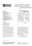
05020-001250 kSPS, 6-Channel, SimultaneousFEATURESFUNCTIONAL BLOCK DIAGRAM6 independent ADCsV DDCONVST ACONVST B CONVST C AV CCDV CCTrue bipolar analog inputsPin-/software-selectable ranges: ±10 V, ±5 V Fast throughput rate: 250 kSPS i CMOS process technologyBUFCLK OSCCONTROL LOGICCS SER/PAR V DRIVE STBYLow power140 mW at 250 kSPS with 5 V supplies V1T/H16-/14-/12-BIT SAROUTPUT DRIVERSDOUT AWide input bandwidthSCLK86.5 dB SNR at 50 kHz input frequency On-chip reference and reference buffersParallel, serial, and daisy-chain interface modes High speed serial interfaceSPI-/QSPI™-/MICROWIRE™-/DSP-compatible Standby mode: 100 μW maximum 64-lead LQFPV2V3 V4 V5T/HT/H T/H T/H BUFBUF16-/14-/12-BIT SAR16-/14-/12-BIT SAR16-/14-/12-BIT SAR16-/14-/12-BIT SAROUTPUT DRIVERSOUTPUT DRIVERSOUTPUT DRIVERSDOUT BDOUT CDATA/ CONTROL LINES RD WRAPPLICATIONSPower line monitoring systems V6T/HV SS16-/14-/12-BIT SARAD7656/AD7657/AD7658AGNDDGNDInstrumentation and control systems Multi-axis positioning systemsGENERAL DESCRIPTIONThe AD7656/AD7657/AD76581 contain six 16-/14-/12-bit, fast, low power, successive approximation ADCs all in the one package that is designed on the i CMOS™ process (industrial CMOS). i CMOS is a process combining high voltage silicon with submicron CMOS and complementary bipolar technol- ogies. It enables the development of a wide range of high performance analog ICs, capable of 33 V operation in a footprint that no previous generation of high voltage partscould achieve. Unlike analog ICs using conventional CMOS processes, i CMOS components can accept bipolar input signals while providing increased performance, which dramatically reduces power consumption and package size.Figure 1.The conversion process and data acquisition are controlled using CONVST signals and an internal oscillator. Three CONVST pins allow independent, simultaneous sampling of the three ADC pairs. The AD7656/AD7657/AD7658 all have a high speed parallel and serial interface, allowing the devices to interface with microprocessors or DSPs. In serial interface mode, the parts have a daisy-chain feature that allows multiple ADCs to connect to a single serial interface. The AD7656/ AD7657/AD7658 can accommodate true bipolar input signals in the ±4 × V REF range and ±2 × V REF range. The AD7656/ AD7657/AD7658 also contain an on-chip 2.5 V reference.PRODUCT HIGHLIGHTSThe AD7656/AD7657/AD7658 feature throughput rates up to 250 kSPS. The parts contain low noise, wide bandwidth, track-and-hold amplifiers that can handle input frequencies up to 12 MHz.1Protected by U.S. Patent No. 6,731,232.Rev. CInformation furnished by Analog Devices is believed to be accurate and reliable. However, no 1. 2. 3.Six 16-/14-/12-bit, 250 kSPS ADCs on board. Six true bipolar, high impedance analog inputs. Parallel and high speed serial interfaces.responsibilityisassumedbyAnalogDevicesforitsuse,norforanyinfringementsofpatentsorother rightsofthirdpartiesthatmayresultfromitsuse.Specificationssubjecttochangewithoutnotice.No license is granted by implication or otherwise under any patent or patent rights of Analog Devices. Trademarksandregisteredtrademarksarethepropertyoftheirrespectiveowners.One Technology Way, P.O. Box 9106, Norwood, MA 02062-9106, U.S.A. Tel: 781.329.4700 Fax: 781.461.3113 ©2006–2010 Analog Devices, Inc. All rights reserved.TABLE OF CONTENTSFeatures (1)Applications (1)Functional Block Diagram (1)General Description (1)Product Highlights (1)Revision History (2)Specifications (3)AD7656 (3)AD7657 (5)AD7658 (7)Timing Specifications (9)Absolute Maximum Ratings (10)Thermal Resistance (10)ESD Caution (10)Pin Configuration and Function Descriptions (11)REVISION HISTORY8/10—Rev. B to Rev. CChanges to t1 Unit in Table 4 (9)Changes to V DD to AV CC Rating in Table 5 (10)Added Power Supply Configuration Section (29)Added Figure 36 (29)V DD to AV CC Typical Performance Characteristics (14)Terminology (18)Theory of Operation (20)Converter Details (20)ADC Transfer Function (21)Reference Section (21)Typical Connection Diagram (21)Driving the Analog Inputs (22)Interface Section (22)Application Hints (29)Layout (29)Power Supply Configuration (29)Outline Dimensions (30)Ordering Guide (30)4/06—Rev. 0 to Rev. AAdded AD7657/AD7658 parts .........................................Universal Changes to Table 1.. (3)Changes to Table 5 (10)3/06—Revision 0: Initial Version1/10—Rev. A to Rev. BChanges to Unit of DC Accuracy Parameter, Table 1 (3)Changes to DC Accuracy Parameter, Table 2 (5)Changes to DC Accuracy Parameter, Table 3 (7)Changes to Terminology Section (18)Updated Outline Dimensions (30)Changes to Ordering Guide (30)Rev. C | Page 2 of 32SPECIFICATIONSAD7656V REF = 2.5 V internal/external, AV CC = 4.75 V to 5.25 V, DV CC = 4.75 V to 5.25 V, V DRIVE = 2.7 V to 5.25 V;For ±4 × V REF range: V DD = 10 V to 16.5 V, V SS = −10 V to −16.5 V; For ±2 × V REF range: V DD = 5 V to 16.5 V, V SS = −5 V to −16.5 V;f SAMPLE = 250 kSPS, T A = T MIN to T MAX, unless otherwise noted.1Table 1.Parameter B Version1 Y Version1 Unit Test Conditions/Comments DYNAMIC PERFORMANCE f IN = 50 kHz sine waveSignal-to-Noise + Distortion (SINAD) 2 Signal-to-Noise Ratio (SNR)2Total Harmonic Distortion (THD)2 8485.58586.5−908485.58586.5−90dB mindB typdB mindB typdB max−92−100−92−100dB typdB typV DD/V SS = ±5 V to ±10 VV DD/V SS = ±12 V to ±16.5 VPeak Harmonic or Spurious Noise (SFDR)2 Intermodulation Distortion (IMD)2 Second-Order TermsThird-Order TermsAperture DelayAperture Delay MatchingAperture Jitter −100−112−10710435−100−112−10710435dB typdB typdB typns maxns maxps typfa = 50 kHz, fb = 49 kHzChannel-to-Channel Isolation2 Full Power Bandwidth −100122−100122dB typMHz typMHz typf IN on unselected channels up to 100 kHz@ −3 dB@ −0.1 dBDC ACCURACYResolutionNo Missing Codes 16151614BitsBits min16 16 Bits min @ 25°CIntegral Nonlinearity2 ±3±1 ±4.5±1LSB maxLSB typPositive Full-Scale Error2Positive Full-Scale Error Matching2 Bipolar Zero-Scale Error2Bipolar Zero-Scale Error Matching2 Negative Full-Scale Error2 Negative Full-Scale Error Matching2 ±0.75±0.35±0.023±0.038±0.75±0.35±0.75±0.35±0.023±0.038±0.75±0.35% FSR max% FSR max% FSR max% FSR max% FSR max% FSR max±0.22% FSR typical±0.004% FSR typical±0.22% FSR typicalANALOG INPUT See Table 8 for min V DD/V SS for each rangeInput Voltage Ranges DC Leakage Current Input Capacitance 3 ±4 × V REF±2 × V REF±11014±4 × V REF±2 × V REF±11014VVμA maxpF typpF typRNG bit/RANGE pin = 0RNG bit/RANGE pin = 1±4 × V REF range when in track±2 × V REF range when in trackREFERENCE INPUT/OUTPUTReference Input Voltage Range DC Leakage Current 2.5/3±12.5/3±1V min/maxμA maxInput Capacitance3Reference Output VoltageLong-Term StabilityReference Temperature Coefficient 18.52.49/2.5115025618.52.49/2.51150256pF typV min/maxppm typppm/°C maxppm/°C typREF EN/DIS = 11,000 hours Rev. C | Page 3 of 32ParameterB Version 1 Y Version 1 Unit Test Conditions/CommentsLOGIC INPUTSInput High Voltage (V INH ) Input Low Voltage (V INL ) 0.7 × V DRIVE 0.3 × V DRIVE 0.7 × V DRIVE 0.3 × V DRIVE V min V max Input Current (I IN ) Input Capacitance (C IN )3 ±1 10 ±1 10 μA max pF max Typically 10 nA, V IN = 0 V or V DRIVELOGIC OUTPUTSOutput High Voltage (V OH ) Output Low Voltage (V OL ) Floating-State Leakage Current Floating-State Output Capacitance 3 V DRIVE − 0.2 0.2 ±1 10 V DRIVE − 0.2 0.2 ±1 10 V min V max μA max pF maxI SOURCE = 200 μA I SINK = 200 μAOutput Coding CONVERSION RATE Twos complement Conversion Time Track-and-Hold Acquisition Time 2, 3 3.1 550 3.1 550 μs max ns max Throughput Rate 250 250 kSPSParallel interface mode onlyPOWER REQUIREMENTS V DD V SS AV CC DV CC V DRIVE 5/15 −5/−15 5 5 3/5 5/15 −5/−15 5 5 3/5 V nom min/max V nom min/max V nom V nomV nom min/max For 4 × V REF range, V DD = 10 V to 16.5 V For 4 × V REF range, V DD = −10 V to −16.5 VI TOTALDigital I/P S = 0 V or V DRIVENormal Mode (Static) 28 28 mA max AV CC = DV CC = V DRIVE = 5.25 V, V DD = 16.5 V, (Includes IAV CC , IV DD , IV SS , IV DRIVE , IDV CC ) V SS = −16.5 VNormal Mode (Operational) 26 26 mA max f SAMPLE = 250 kSPS, AV CC = DV CC = V DRIVE = 5.25 V, (Includes IAV CC , IV DD , IV SS , IV DRIVE , IDV CC ) V DD = 16.5 V, V SS = −16.5 VI SS (Operational) I DD (Operational) Partial Power-Down Mode 0.25 0.25 7 0.25 0.25 7mA max mA max mA max V SS = −16.5 V, f SAMPLE = 250 kSPS V DD = 16.5 V, f SAMPLE = 250 kSPSAV CC = DV CC = V DRIVE = 5.25 V, V DD = 16.5 V, V SS = −16.5 VFull Power-Down Mode (STBY Pin) 8080μA maxSCLK on or off, AV CC = DV CC = V DRIVE = 5.25 V, V DD = 16.5 V, V SS = −16.5 VPower DissipationAV CC = DV CC = V DRIVE = 5.25 V, V DD = 16.5 V, V SS = −16.5 V Normal Mode (Static)143 143 mW max Normal Mode (Operational) Partial Power-Down ModeFull Power-Down Mode (STBY Pin)140 35 100140 35 100mW max mW max μW maxf SAMPLE = 250 kSPS1 2 3Temperature ranges are as follows: B version is −40°C to +85°C and Y version is −40°C to +125°C.See the Terminology section.Sample tested during initial release to ensure compliance.Rev. C | Page 4 of 32AD7657V REF = 2.5 V internal/external, AV CC = 4.75 V to 5.25 V, DV CC = 4.75 V to 5.25 V, V DRIVE = 2.7 V to 5.25 V;For ±4 × V REF range: V DD = 10 V to 16.5 V, V SS = −10 V to −16.5 V; For ±2 × V REF range: V DD = 5 V to 16.5 V, V SS = −5 V to −16.5 V;f SAMPLE = 250 kSPS, T A = T MIN to T MAX, unless otherwise noted.1Table 2.Parameter B Version1 Y Version1 Unit Test Conditions/Comments DYNAMIC PERFORMANCE f IN = 50 kHz sine waveSignal-to-Noise + Distortion (SINAD) 2 Signal-to-Noise Ratio (SNR)2Total Harmonic Distortion (THD)2Peak Harmonic or Spurious Noise (SFDR)2 Intermodulation Distortion (IMD)2 Second-Order TermsThird-Order TermsAperture DelayAperture Delay MatchingAperture Jitter 81.582.583.5−90−92−100−109−1041043581.582.583.5−89−92−100−109−10410435dB mindB mindB typdB maxdB typdB typdB typdB typns maxns maxps typfa = 50 kHz, fb = 49 kHzChannel-to-Channel Isolation2 Full Power Bandwidth −100122−100122dB typMHz typMHz typf IN on unselected channels up to 100 kHz@ −3 dB@ −0.1 dBDC ACCURACYResolutionNo Missing Codes Integral Nonlinearity2 1414±1.5±11414±1.5±1BitsBits minLSB maxLSB typPositive Full-Scale Error2Positive Full-Scale Error Matching2 Bipolar Zero-Scale Error2Bipolar Zero-Scale Error Matching2 Negative Full-Scale Error2 Negative Full-Scale Error Matching2 ±0.75±0.3±0.0305±0.0427±0.75±0.3±0.75±0.3±0.0305±0.0427±0.75±0.3% FSR max% FSR max% FSR max% FSR max% FSR max% FSR max±0.183% FSR typical±0.015 % FSR typical±0.183% FSR typicalANALOG INPUT See Table 8 for min V DD/V SS for each rangeInput Voltage Ranges DC Leakage Current Input Capacitance 3 ±4 × V REF±2 × V REF±11014±4 × V REF±2 × V REF±11014VVμA maxpF typpF typRNG bit/RANGE pin = 0RNG bit/RANGE pin = 1±4 × V REF range when in track±2 × V REF range when in trackREFERENCE INPUT/OUTPUTReference Input Voltage Range DC Leakage Current 2.5/3±12.5/3±1V min/maxμA maxInput Capacitance3Reference Output VoltageLong-Term StabilityReference Temperature Coefficient 18.52.49/2.5115025618.52.49/2.51150256pF typV min/maxppm typppm/°C maxppm/°C typREF EN/DIS = 11,000 hoursLOGIC INPUTSInput High Voltage (V INH) Input Low Voltage (V INL) 0.7 × V DRIVE0.3 × V DRIVE0.7 × V DRIVE0.3 × V DRIVEV minV maxInput Current (I IN) Input Capacitance (C IN)3 ±110±110μA maxpF maxTypically 10 nA, V IN = 0 V or V DRIVE Rev. C | Page 5 of 32ParameterB Version 1 Y Version 1 Unit Test Conditions/Comments LOGIC OUTPUTSOutput High Voltage (V OH ) Output Low Voltage (V OL ) Floating-State Leakage Current Floating-State Output Capacitance 3 V DRIVE − 0.2 0.2 ±1 10 V DRIVE − 0.2 0.2 ±1 10 V min V max μA max pF maxI SOURCE = 200 μA I SINK = 200 μAOutput Coding CONVERSION RATE Twos complement Conversion Time Track-and-Hold Acquisition Time 2, 3 3.1 550 3.1 550 μs max ns max Throughput Rate 250 250 kSPSParallel interface mode onlyPOWER REQUIREMENTS V DD V SS AV CC DV CC V DRIVE 5/15 −5/−15 5 5 3/5 5/15 −5/−15 5 5 3/5 V nom min/max V nom min/max V nom V nomV nom min/max For 4 × V REF range, V DD = 10 V to 16.5 V For 4 × V REF range, V DD = −10 V to −16.5 VI TOTALDigital I/P S = 0 V or V DRIVENormal Mode (Static) 28 28 mA max AV CC = DV CC = V DRIVE = 5.25 V, V DD = 16.5 V, (Includes IAV CC , IV DD , IV SS , IV DRIVE , IDV CC ) V SS = −16.5 VNormal Mode (Operational) 26 26 mA max f SAMPLE = 250 kSPS, AV CC = DV CC = V DRIVE = 5.25 V, (Includes IAV CC , IV DD , IV SS , IV DRIVE , IDV CC ) V DD = 16.5 V, V SS = −16.5 VI SS (Operational) I DD (Operational) Partial Power-Down Mode 0.25 0.25 7 0.25 0.25 7mA max mA max mA max V SS = −16.5 V, f SAMPLE = 250 kSPS V DD = 16.5 V, f SAMPLE = 250 kSPSAV CC = DV CC = V DRIVE = 5.25 V, V DD = 16.5 V, V SS = −16.5 VFull Power-Down Mode (STBY Pin) 8080μA maxSCLK on or off, AV CC = DV CC = V DRIVE = 5.25 V, V DD = 16.5 V, V SS = −16.5 VPower DissipationAV CC = DV CC = V DRIVE = 5.25 V, V DD = 16.5 V, V SS = −16.5 V Normal Mode (Static)143 143 mW max Normal Mode (Operational) Partial Power-Down ModeFull Power-Down Mode (STBY Pin)140 35 100140 35 100mW max mW max μW maxf SAMPLE = 250 kSPS1 23Temperature ranges are as follows: B version is −40°C to +85°C and Y version is −40°C to +125°C. See the Terminology section. Sample tested during initial release to ensure compliance.Rev. C | Page 6 of 32AD7658V REF = 2.5 V internal/external, AV CC = 4.75 V to 5.25 V, DV CC = 4.75 V to 5.25 V, V DRIVE = 2.7 V to 5.25 V;For ±4 × V REF range: V DD = 10 V to 16.5 V, V SS = −10 V to −16.5 V; For ±2 × V REF range: V DD = 5 V to 16.5 V, V SS = −5 V to −16.5 V;f SAMPLE = 250 kSPS, T A = T MIN to T MAX, unless otherwise noted.1Table 3.Parameter B Version1 Y Version1 Unit Test Conditions/Comments DYNAMIC PERFORMANCE f IN = 50 kHz sine waveSignal-to-Noise + Distortion (SINAD) 2 Total Harmonic Distortion (THD)2Peak Harmonic or Spurious Noise (SFDR)2 Intermodulation Distortion (IMD)2 Second-Order TermsThird-Order TermsAperture DelayAperture Delay MatchingAperture Jitter 7373.5−88−92−97−106−101104357373.5−88−92−97−106−10110435dB mindB typdB maxdB typdB typdB typdB typns maxns maxps typfa = 50 kHz, fb = 49 kHzChannel-to-Channel Isolation2 Full Power Bandwidth −100122−100122dB typMHz typMHz typf IN on unselected channels up to 100 kHz@ −3 dB@ −0.1 dBDC ACCURACYResolutionNo Missing Codes Differential Nonlinearity Integral Nonlinearity2 1212±0.7±11212±0.7±1BitsBits minLSB maxLSB maxPositive Full-Scale Error2Positive Full-Scale Error Matching2 Bipolar Zero-Scale Error2Bipolar Zero-Scale Error Matching2 Negative Full-Scale Error2 Negative Full-Scale Error Matching2 ±0.75±0.366±3±3±0.75±0.366±0.75±0.366±3±3±0.75±0.366% FSR max% FSR maxLSB maxLSB max% FSR max% FSR max±0.244% FSR typical±0.0488% FSR typical±0.244% FSR typicalANALOG INPUT See Table 8 for min V DD/V SS for each rangeInput Voltage Ranges DC Leakage Current Input Capacitance 3 ±4 × V REF±2 × V REF±11014±4 × V REF±2 × V REF±11014VVμA maxpF typpF typRNG bit/RANGE pin = 0RNG bit/RANGE pin = 1±4 × V REF range when in track±2 × V REF range when in trackREFERENCE INPUT/OUTPUTReference Input Voltage Range DC Leakage Current 2.5/3±12.5/3±1V min/maxμA maxInput Capacitance3Reference Output VoltageLong-Term StabilityReference Temperature Coefficient 18.52.49/2.5115025618.52.49/2.51150256pF typV min/maxppm typppm/°C maxppm/°C typREF EN/DIS = 11,000 hoursLOGIC INPUTSInput High Voltage (V INH) Input Low Voltage (V INL) 0.7 × V DRIVE0.3 × V DRIVE0.7 × V DRIVE0.3 × V DRIVEV minV maxInput Current (I IN) Input Capacitance (C IN)3 ±110±110μA maxpF maxTypically 10 nA, V IN = 0 V or V DRIVE Rev. C | Page 7 of 32ParameterB Version 1 Y Version 1 Unit Test Conditions/Comments LOGIC OUTPUTSOutput High Voltage (V OH ) Output Low Voltage (V OL ) Floating-State Leakage Current Floating-State Output Capacitance 3 V DRIVE − 0.2 0.2 ±1 10 V DRIVE − 0.2 0.2 ±1 10 V min V max μA max pF maxI SOURCE = 200 μA I SINK = 200 μAOutput Coding CONVERSION RATE Twos complement Conversion Time Track-and-Hold Acquisition Time 2, 3 3.1 550 3.1 550 μs max ns max Throughput Rate 250 250 kSPSParallel interface mode onlyPOWER REQUIREMENTS V DD V SS AV CC DV CC V DRIVE 5/15 −5/−15 5 5 3/5 5/15 −5/−15 5 5 3/5 V nom min/max V nom min/max V nom V nomV nom min/max For 4 × V REF range, V DD = 10 V to 16.5 V For 4 × V REF range, V DD = −10 V to −16.5 VI TOTALDigital I/P S = 0 V or V DRIVENormal Mode (Static) 28 28 mA max AV CC = DV CC = V DRIVE = 5.25 V, V DD = 16.5 V, (Includes IAV CC , IV DD , IV SS , IV DRIVE , IDV CC ) V SS = −16.5 VNormal Mode (Operational) 26 26 mA max f SAMPLE = 250 kSPS, AV CC = DV CC = V DRIVE = 5.25 V, (Includes IAV CC , IV DD , IV SS , IV DRIVE , IDV CC ) V DD = 16.5 V, V SS = −16.5 VI SS (Operational) I DD (Operational) Partial Power-Down Mode 0.25 0.25 7 0.25 0.25 7mA max mA max mA max V SS = −16.5 V, f SAMPLE = 250 kSPS V DD = 16.5 V, f SAMPLE = 250 kSPSAV CC = DV CC = V DRIVE = 5.25 V, V DD = 16.5 V, V SS = −16.5 VFull Power-Down Mode (STBY Pin) 8080μA maxSCLK on or off, AV CC = DV CC = V DRIVE = 5.25 V, V DD = 16.5 V, V SS = −16.5 VPower DissipationAV CC = DV CC = V DRIVE = 5.25 V, V DD = 16.5 V, V SS = −16.5 V Normal Mode (Static)143 143 mW max Normal Mode (Operational) Partial Power-Down ModeFull Power-Down Mode (STBY Pin)140 35 100140 35 100mW max mW max μW maxf SAMPLE = 250 kSPS1 23Temperature ranges are as follows: B version is −40°C to +85°C and Y version is −40°C to +125°C See the Terminology section. Sample tested during initial release to ensure compliance.Rev. C | Page 8 of 3205020-002TIMING SPECIFICATIONSAV CC /DV CC = 4.75 V to 5.25 V, V DD = 5 V to 16.5 V, V SS = −5 V to −16.5 V, V DRIVE = 2.7 V to 5.25 V, V REF = 2.5 V internal/external, T A = T MIN to T MAX , unless otherwise noted.1Table 4.Limit at T MIN,T MAXParameterV DRIVE < 4.75V V DRIVE = 4.75V to 5.25V Unit DescriptionPARALLEL MODE t CONVERT t QUIET3 1503 150 μs typ ns min Conversion time, internal clockMinimum quiet time required between bus relinquish and start of next conversion t ACQ t 10 t 1t WAKE-UP550 25 60 2 25550 25 60 2 25 ns min ns min ns max ms max μs max Acquisition timeMinimum CONVST low pulse CONVST high to BUSY highSTBY rising edge to CONVST rising edge Partial power-down modePARALLEL WRITE OPERATION t 11 t 12 t 13 t 14 t 15 15 0 5 5 515 0 5 5 5 ns min ns min ns min ns min ns min WR pulse width CS to WR setup time CS to WR hold timeData setup time before WR rising edge Data hold after WR rising edge PARALLEL READ OPERATION t 2 t 3 t 4 t 5 t 6 t 7 t 8 t 9 0 0 0 45 45 10 12 6 0 0 0 36 36 10 12 6 ns min ns min ns min ns min ns max ns min ns max ns min BUSY to RD delay CS to RD setup time CS to RD hold time RD pulse widthData access time after RD falling edge Data hold time after RD rising edge Bus relinquish time after RD rising edge Minimum time between readsSERIAL INTERFACE f SCLK t 16 18 12 18 12 MHz max ns max Frequency of serial read clockDelay from CS until SDATA three-state disabledt 17 t 18 t 19 t 20 t 21 2 22 0.4 t SCLK 0.4 t SCLK 10 18220.4 t SCLK 0.4 t SCLK 10 18ns max ns min ns min ns min ns maxData access time after SCLK rising edge/CS falling edge SCLK low pulse width SCLK high pulse widthSCLK to data valid hold time after SCLK falling edge CS rising edge to SDATA high impedance1 2Sample tested during initial release to ensure compliance. All input signals are specified with t R = t F = 5 ns (10% to 90% of V DD ) and timed from a voltage level of 1.6 V. A buffer is used on the data output pins for this measurement.TO OUTPUTPINFigure 2. Load Circuit for Digital Output Timing SpecificationRev. C | Page 9 of 32ABSOLUTE MAXIMUM RATINGS T A = 25°C, unless otherwise noted.Stresses above those listed under Absolute Maximum Ratingsmay cause permanent damage to the device. This is a stressrating only; functional operation of the device at these or anyother conditions above those indicated in the operationalsection of this specification is not implied. Exposure to absolutemaximum rating conditions for extended periods may affectdevice reliability.THERMAL RESISTANCEθJA is specified for the worst-case conditions, that is, a devicesoldered in a circuit board for surface-mount packages. Thesespecifications apply to a four-layer board.Table 6. Thermal ResistancePackage Type64-Lead LQFPθJA45θJC11Unit°C/WESD CAUTION12If the analog inputs are being driven from alternative V DD and V SS supplycircuitry, a 240 Ω series resistor should be placed on the analog inputs.Transient currents of up to 100 mA do not cause SCR latch-up.Rev. C | Page 10 of 32R E F I N /R E F O U TW R /R E F E N /D I SS E R /P A R /S E LR E F C A P CR E F C A P BR E F C A P AH /S S E LA G N DA G N DA G N DA G N DA G N DA G N DD B 15A V C CD B 0/SE L AC O N V S T AB U S YC O N V S T CC O N V S T BS T B YD G N DW /BR DA V C CV D DR E S E TR A N G EA G N DC SD V C CV S S05020-003PIN CONFIGURATION AND FUNCTION DESCRIPTIONS64 63 62 61 60 59 5857 56 55 54 53 52 51 50 49DB14/REFBUF EN/DIS148 V6 DB13 DB12 DB11DB10/DOUT C DB9/DOUT B DB8/DOUT ADGND V DRIVE2 3 4 5 6 7 8 9PIN 1AD7656/AD7657/AD7658TOP VIEW (Not to Scale)47 AV CC 46 AV CC 45 V5 44 AGND 43 AGND 42 V4 41 AV CC 40 AV CC DB7/HBEN/DCEN 10DB6/SCLK 11 DB5/DCIN A 12 DB4/DCIN B 13 DB3/DCIN C 14 DB2/SEL C 15DB1/SEL B 16Table 7. Pin Function Descriptions 17 18 19 20 21 22 23 24 25 26 27 28 29 30 31 32Figure 3. Pin Configuration39 V3 38 AGND 37 AGND 36 V2 35 AV CC 34 AV CC 33 V1Pin No. 54, 56, 58 33, 36, 39,42, 45, 48 32, 37, 38, 43,44, 49, 52, 53, 55, 57, 592698, 2534, 35, 40, 41, 46, 47, 50, 6023, 22, 21Mnemonic REFCAPA, REFCAPB,REFCAPC V1 to V6AGNDDV CCV DRIVEDGNDAV CCCONVST A,CONVST B, CONVST C DescriptionDecoupling capacitors are connected to these pins. This decouples the reference buffer for each ADC pair. Each REFCAP pin should be decoupled to AGND using 10 μF and 100 nF capacitors. Analog Input 1 to 6. These are six single-ended analog inputs. In hardware mode, the analog input range on these channels is determined by the RANGE pin. In software mode, it is determined by Bit RNGC to Bit RNGA of the control register (see Table 10). Analog Ground. Ground reference point for all analog circuitry on the AD7656/AD7657/AD7658. All analog input signals and any external reference signal should be referred to this AGND voltage. All 11 of these AGND pins should be connected to the AGND plane of a system. The AGND and DGND voltages should ideally be at the same potential and must not be more than 0.3 V apart,even on a transient basis. Digital Power, 4.75 V to 5.25 V. The DV CC and AV CC voltages should ideally be at the same potential and must not be more than 0.3 V apart, even on a transient basis. This supply should be decoupledto DGND, and 10 μF and 100 nF decoupling capacitors should be placed on the DV CC pin. Logic Power Supply Input. The voltage supplied at this pin determines the operating voltage of the interface. Nominally at the same supply as the supply of the host interface. This pin should be decoupled to DGND, and 10 μF and 100 nF decoupling capacitors should be placed on the V DRIVE pin. Digital Ground. This is the ground reference point for all digital circuitry on the AD7656/AD7657/AD7658. Both DGND pins should connect to the DGND plane of a system. The DGND and AGND voltages should ideally be at the same potential and must not be more than 0.3 V apart, even on a transient basis. Analog Supply Voltage, 4.75 V to 5.25 V. This is the supply voltage for the ADC cores. The AV CC and DV CC voltages should ideally be at the same potential and must not be more than 0.3 V apart, even on a transient basis. These supply pins should be decoupled to AGND, and 10 μF and 100 nF decoupling capacitors should be placed on the AV CC pins. Conversion Start Input A, B, C. These logic inputs are used to initiate conversions on the ADC pairs. CONVST A is used to initiate simultaneous conversions on V1 and V2. CONVST B is used to initiatesimultaneous conversions on V3 and V4. CONVST C is used to initiate simultaneous conversions on V5 and V6. When CONVSTx switches from low to high, the track-and-hold switch on the selected ADC pair switches from track to hold and the conversion is initiated. These inputs can also be used to place the ADC pairs into partial power-down mode.Rev. C | Page 11 of 32。

AD7656—16位同步采样双极ADC转换器功能:6路独立的16位AD6路真双极模拟量输入引脚/软件可选择的范围:±10V,±5V快速通过率250KSPS指定Vcc为4.5V~5.5V低功耗以5V 供应250 kSPS的160 mW宽的输入带宽: 输入频率为100kHz时信噪比为85dB在片参考和参考缓冲器并行和串行接口高速串行接口SPI/ QSPI/μWire/DSP可兼容无流水线延迟备用模式:最大0.5μA64LQFP封装应用电力线检测系统仪器和控制系统多轴定位系统一般描述AD7656芯片包含6路16位快速、低功耗、逐步逼近ADC。
元件工作电源4.5V~5.5V,具有250kSPS通过率特性。
元件具有低噪音、宽带宽跟踪保持放大器,能够操作输入频率达到8MHz。
转换过程和数据采集由 CONVST 信号和一个内部振荡器控制。
三个CONVST引脚允许三对ADC独立的同时采样。
AD7656具有高速的并行和串行接口,可以与微处理器和DSP接口。
AD7656具有菊花链特性,允许多个ADC与一个串行接口连接。
元件没有流水线延迟。
AD7656在±10V范围内能提供真双极的输入信号。
AD7656包含一个2.5V内部参考电压,也能采用一个外部考电压,如果V REF引脚供应一个3V外部叁考电压, ADC能供给真双极±12V模拟量输入范围。
参照这±12V输入范围,需要给V DD和V SS提供±12V电压。
产品特点1 6路16位250kSPS ADC2 6路真双极高阻抗模拟量输入3 具有一个并行和一个高速串行接口。
引脚功能描述术语积分非线性这是从一条直线横传过ADC传递函数终点的最大的偏差。
传递函数终点是零刻度时,1/2LSB点低于最初代码转换,是满刻度时,1/2LSB点超出最后代码转换。
差分非线性这是一个在ADC转换中任何两个邻近代码的LSB转换的测量值与理论值差。


2 AD7656的特性及引脚功能2.1 AD7656的特性图1示出AD7656的功能框图。
AD7656的主要特性如下:●6通道16-bit逐次逼近型ADC;●最大吞吐率为250kS/s;●A Vcc范围为4.75V-5.25V;●低功耗:在供电电压为5V、采样速率为250kS/s时的功耗为160mW;●宽带宽输入:输入频率为50kHz时的信噪比(SNR)为85dB;●片上有2.5V基准电压源和基准缓冲器;●有并行和串行接口;●与SPI/QSPI/μWire/DSP兼容的高速串行接口;●可通过引脚或软件方式设定输入电压范围(±10V,±5V);●采用iCMOS工艺技术;●64引脚QFP。
2.2 AD7656的引脚功能REFCAPA、REFCAPB、REFCAPC是参考电压引脚,这几个引脚应该接去耦电容器来减小每1个ADC 通道参考缓冲器的衰减。
V1一V6是模拟输入1-6引脚,它们是模拟前端输入,对应通道的输入范围取决于RANGE引脚的定义。
AGND是模拟地,所有的模拟输入信号和外部参考信号都要用AGND。
DVcc是5V数字电源端。
VDRIVE是逻辑电源输入,该引脚的电压取决于内部参考电压,应接10μF或100μF的去耦电容器。
DGND是数字地,它是数字电路的参考点。
A Vcc是模拟电压输入(4.5V-5.5V),它只给ADC的内核供电。
CONVSTA/B/C是转换使能逻辑输入,每对有其相关的CONVST信号,用来启动每对或每4个或6个ADC同步采样。
CS是片选信号,逻辑低电平时使能。
RD是读信号,逻辑低电平时使能。
WR/PEFEN/DIS是写数据/参考使能/非使能。
BUSY是忙信号输出,当转换开始时为高电平,并且在转换结束前一直为高电平。
SER/PAR是串行/并行选择输入信号。
低电平时选择并行接口模式,高电平时选择串行接口模式。
DB[0]/SEL A是数据0位/选择输出A路。
AD7656—16位同步采样双极ADC转换器功能:6路独立的16位AD6路真双极模拟量输入引脚/软件可选择的范围:±10V,±5V快速通过率250KSPS指定Vcc为4.5V~5.5V低功耗以5V 供应250 kSPS的160 mW宽的输入带宽: 输入频率为100kHz时信噪比为85dB在片参考和参考缓冲器并行和串行接口高速串行接口SPI/ QSPI/μWire/DSP可兼容无流水线延迟备用模式:最大0.5μA64LQFP封装应用电力线检测系统仪器和控制系统多轴定位系统一般描述AD7656芯片包含6路16位快速、低功耗、逐步逼近ADC。
元件工作电源4.5V~5.5V,具有250kSPS通过率特性。
元件具有低噪音、宽带宽跟踪保持放大器,能够操作输入频率达到8MHz。
转换过程和数据采集由 CONVST 信号和一个内部振荡器控制。
三个CONVST引脚允许三对ADC独立的同时采样。
AD7656具有高速的并行和串行接口,可以与微处理器和DSP接口。
AD7656具有菊花链特性,允许多个ADC与一个串行接口连接。
元件没有流水线延迟。
AD7656在±10V范围内能提供真双极的输入信号。
AD7656包含一个2.5V内部参考电压,也能采用一个外部考电压,如果V REF引脚供应一个3V外部叁考电压, ADC能供给真双极±12V模拟量输入范围。
参照这±12V输入范围,需要给V DD和V SS提供±12V电压。
产品特点1 6路16位250kSPS ADC2 6路真双极高阻抗模拟量输入3 具有一个并行和一个高速串行接口。
引脚功能描述术语积分非线性这是从一条直线横传过ADC传递函数终点的最大的偏差。
传递函数终点是零刻度时,1/2LSB点低于最初代码转换,是满刻度时,1/2LSB点超出最后代码转换。
差分非线性这是一个在ADC转换中任何两个邻近代码的LSB转换的测量值与理论值差。
AD7656的原理及在继电保护产品中的应用1 AD7656的性能简介AD7656是高集成度、6通道、16bit逐次逼近(SAR)型ADC,它具有最大4 LSBS INL和每通道达250kSPS的采样率,并且在片内包含一个2.5V内部基准电压源和基准缓冲器。
该器件仅有典型值160mW的功耗,比最接近的同类双极性输入ADC的功耗降低了60%。
AD7656包含一个低噪声、宽带采样保持放大器(T/H),以便处理输入频率高达8MHz的信号。
该AD7656还具有高速并行和串行接口,可以与微处理器(MCU)或数字信号处理器(DSP)连接。
AD7656在串行接口方式下,能提供一个菊花链连接方式,以便把多个ADC连接到一个串行接口上。
AD7656采用具有ADI专利技术的iCMOS(工业CMOS)工艺。
iCMOS 工艺是一种高压半导体工艺与亚微米CMOS(互补金属氧化物半导体)和互补双极型工艺相结合的制造上艺。
它能开发出承受30V电源电压的多种高性能模拟IC,并且其小封装尺寸是任何其他同类高电压IC都未曾达到的。
与使用传统CMOS工艺的模拟IC不同,iCMOS器件能承受高电源电压,同时提高性能、显著降低功耗和缩小封装尺寸。
AD7656是使用该种工艺设计制造的产品,所以非常适合在继电保护、电机控制等工业领域使用。
图1是AD7656的内部原理框图。
2 AD7656的工作原理AD7656足具有独立的六通道逐次逼近型(SAR)的模数转换器,转换处理和数据的精度是通过CONVST信号和一个内部晶振控制的。
3个CONVST管脚允许3路ADC对独立同步采样。
当3个CONVST管脚连接到一起时,就可以进行6个通道的同步采样。
AD7656具有高速的并行和串行接口,允许其与Microprocessors和DSP进行接口。
当使用串行接口模式时,AD7656具有的菊花链特性允许多个ADC和一个串行接口连接。
由于在电力继电保护产品中以并行接口连接设计为主,所以下面将以并行接口的连接方式介绍其工作原理。
250 kSPS 、六通道、同步采样、双极性16/14/12-位 ADCAD7656/AD7657/AD7658Rev. D Information furnished by Analog Devices is believed to be accurate and reliable. However , no responsibility is assumed by Analog Devices for its use, nor for any infringements of patents or other rights of third parties that may result from its use. Speci cations subject to change without notice. No license is granted by implication or otherwise under any patent or patent rights of Analog Devices. T rademarks and registered trademarks are the property of their respective owners.One Technology Way, P.O.Box 9106, Norwood, MA 02062-9106, U.S.A.Tel: 781.329.4700 Fax: 781.461.3113 2006–2012 Analog Devices, Inc. All rights reserved.功能框图V SSDGNDV DDREFCONVST ACONVST B CONVST C OUTPUT DRIVERSOUTPUT DRIVERSOUTPUT DRIVERSOUTPUT DRIVERSCONTROL LOGICBUFBUFBUFAGNDT/HT/H T/H T/HT/HT/HCLK OSCAV CCDV CCV1V2V3V4V5V6SER/PAR CSV DRIVE STBYDOUT ADOUT BDOUT C SCLKRD WRDATA/CONTROL LINES 05020-001AD7656/AD7657/AD765816-/14-/12-BIT SAR16-/14-/12-BIT SAR16-/14-/12-BIT SAR16-/14-/12-BIT SAR16-/14-/12-BIT SAR16-/14-/12-BIT SAR图1.-1受美国专利第6,731,232号保护。