Microchip连接电网的太阳能微逆变器220V参考设计
- 格式:doc
- 大小:11.51 KB
- 文档页数:4

一、简介AND220系列的正弦波逆变电源是新一代专用电源主要针对中国电力、汽车供电系统的特点和要求设计制造,采用先进的正弦波脉宽调制(SPWM)技术,具有可靠性高、保护功能全、波形失真小、功率大等优点。
适合对供电设备高质量、高可靠性的要求。
二、应用AND220系列的正弦波逆变电源输入直流电压为220V DC,输出为交流220V AC。
主要为发电厂、电力系统、化工、冶金等重要场合提供不间断电力。
在有直流屏的发电厂或通信系统采用逆变电源与常规不间断电源(UPS)相比,前者有一下优点:1、避免蓄电池的重复投资,减少系统的维护,降低系统运行成本;2、由于直流屏通常采用阀控式密封电池,电池的浮充寿命较长,因此采用直流动力加逆变电源,其供电可靠性和寿命大大提高;3、由于电厂的直流电池屏容量均较大,因此采用逆变电源供电时,在市电断电后可提供较长的交流供电时间;4、正弦波逆变电源的应用消除了直接使用市电和UPS电源所产生的不利因素,从根本上避免了由于市电不稳、供电中断、杂音干扰和雷电侵入等造成的危害。
三、保护功能:四、安装步骤及使用方法:端子排接线指示:上面接线柱依次为:“+”:直流输入的正极,“-”:直流输入的负极,注意正负及切勿接反。
“L”:旁路输入的火线,“N”:旁路输入的零线;“地”:交流输入的接地线。
“L”:交流输出的火线,“N”:交流输出的零线;“地”:交流输出的接地线.1、开箱时,请检查箱体是否有损坏情况,若箱体有明显变形,请立即与供应商联系。
2、确认前面板上启动开关处于“OFF”位置。
机箱后面的直流开关也处于“OFF”位置。
3、请按照逆变器后面输入标示正确将直流线接入端子,“+”“-”切勿接反!4、开机:先接通电源的直流输入,将机箱后面的直流空气开关置于“ON”位置,然后把电源前面板上的启动开关置于“ON”位置,这时启动开关上面的市电灯亮,表示旁路输入正常工作。
电源的“逆变”指示灯发光,表示逆变器工作正常。


© 2012 Microchip Technology Inc.DS01444A_CN 第 1页AN1444作者:Alex Dumais 和Sabarish Kalyanaraman Microchip Technology Inc.简介风力发电系统和光伏(PV )发电系统等可再生资源使用方便且前景广阔,在过去几年获得了大量关注。
太阳能系统具有很多优势,例如:•清洁的可再生能源,可替代煤、石油和核能产生的能量•可降低/消除用电费用•用于制造PV 电池板的硅是地球上含量第二多的元素•能够为边远地点提供电能随着晶体电池板制造能力的增强,总体制造成本随之降低,PV 电池板的效率也得以提高,因此近来对太阳能系统的需求不断增长。
使太阳能需求增长的其他原 因包括:PV 技术经过验证且可靠,PV 模块具有30年以上的保修期,以及政府的鼓励措施。
太阳能逆变器系统有两个主要要求:从PV 电池板收集可用能量,以及将与电网电压同相的正弦电流注入电网。
为了从PV 电池板收集能量,需要使用最大功率点追踪(Maximum Power Point Tracking ,MPPT )算法。
该算法决定了在任何给定时间可从PV 模块获取的最大功率。
与电网接口要求太阳能逆变器系统符合公共事业公司指定的特定标准。
这些标准(如EN61000-3-2、IEEE1547和美国国家电气规范(NEC )690)涉及电源质量、安全、接地和孤岛情况检测。
太阳能电池的特性要开始开发太阳能微型逆变器系统,了解太阳能电池的不同特性非常重要。
PV 电池是半导体器件,其电气特性与二极管相似。
但是,PV 电池是电力来源,当其受到光(如太阳光)照射时会成为电流源。
目前最常见的技术是单晶硅模块和多晶硅模块。
PV 电池的模型如图1所示。
Rp 和Rs 为寄生电阻,在理想情况下分别为无穷大和零。
图1:PV 电池的简化模型RpRsVoIoPV 电池的表现会因其尺寸或与其连接的负载的类型,以及太阳光的强度(照度)而有所不同。

微型光伏发电逆变器的设计摘要目前,人类社会发展迅速,对能源的需求不断加大,能源危机和环境保护成了21世纪的主题。
太阳能具有无限性,清洁性等特点,如果能加以利用,对人类以后的发展和延续由很重要的意义。
在此背景下,本设计基于TMS320F240对光伏发电并网逆变器做出了分析和研究。
本设计首先介绍了国内外光伏发电的现状,分析了光伏发电的工作原理,然后对主电路结构进行分析和选择,最终确定前级采用Boost升压电路以及后级采用全桥逆变电路,逆变主电路采用无变压器绝缘的两级拓扑结构。
控制方法采用滞环反馈调节。
分析了太阳能电池的工作原理,确定了采用扰动观测法实现最大功率点跟踪(MPPT)的方法。
接着论述了孤岛效应的产生原因和危害,确定了采用周期性扰动正反馈频率漂移(AFDPF)孤岛检测方法。
对系统进行了软硬件的设计,最后利用MATLAB软件对系统部分指标进行了仿真,满足了部分要求。
本次设计能够部分解决地区供电难,社会能源短缺问题,对社会发展和稳定有重大现实意义。
关键词:太阳能,光伏并网逆变器,最大功率点跟踪,孤岛检测,MATLABThe Design of Photovoltaic InverterABSTRACTAt present, the development of human beings growing demand for energy, the energy crisis and environmental pollution have become the theme of this century. In this background, this paper use the solar energy, based on TMS320F240 is designed 800 w miniature grid-connected photovoltaic inverter.At first, this paper analyzes the main circuit structure of system, before the final level using the Boost booster circuit, and the latter adopts full bridge inverter circuit working principle of inverter main circuit adopts the two levels of topological structure of transformer insulation. Then analyzed the working principle of solar cells, determines the disturbance observation method is used to achieve maximum power point tracking (MPPT) method. Then discusses the causes and harm of islanding, determines the periodic disturbance using positive feedback frequency drift island (AFDPF) detection method.Finally, the system hardware and software design, and on the part of the performance of the MATLAB simulation, to verify the part of the performance of the system.KEY WORDS:The solar energy,Photovoltaic grid-connected inverter,Maximum power point tracing,Island detection,MATLAB目录前言 (1)第1章绪论 (2)1.1 微型光伏发电逆变器国内外研究动态 (2)1.2 选题的依据和意义 (2)1.3 基本内容和解决重点问题 (3)1.4 研究进度 (3)1.5 主要内容 (3)第2章控制系统总体设计 (4)2.1 光伏逆变系统的工作过程 (5)2.2 光伏并网逆变系统的性能指标和参数要求 (6)2.2.1 逆变器性能指标 (6)2.2.2 逆变器参数要求 (6)2.3 光伏并网逆变系统的控制方案 (7)2.3.1 系统的整体控制方案 (7)第3章控制系统硬件设计 (10)3.1 控制系统的整体构成 (10)3.2 控制系统中变量分析 (10)3.2.1 变步长扰动观察法实现最大功率点跟踪 (10)3.2.2 孤岛效应及其检测方法 (12)3.3控制系统中所用硬件设备的选择 (13)3.3.1 Boost电路设计 (13)3.3.2 逆变电路设计 (15)3.3.3 驱动电路的设计 (17)3.3.4 控制电路的设计 (18)第4章控制系统的软件设计 (19)4.1 MATLAB简介 (19)4.2控制系统整体设计 (20)4.3 DSP 锁相环节软件设计 (20)第5章系统仿真 (22)5.1电流跟踪型逆变器仿真 (22)5.2光伏阵列的仿真 (25)5.3扰动观察法模型仿真 (28)第6章总结与展望 (31)6.1本设计主要完成的工作 (31)6.2控制系统的性能和优缺点 (31)6.3控制系统设计过程中的技术难点 (32)6.4控制系统还需改进的地方 (32)谢辞 (33)参考文献 (34)外文翻译资料 (36)前言本课题主要针对目前能源问题而设计,能源问题一直关乎人类生存和发展,是人类能否延续下去的关键。
小功率光伏逆变器设计韩 翠(中国矿业大学 计算机科学与技术学院 江苏 徐州 221000)摘 要: 光伏发电系统是由光伏电池板产生电能并将其转换成负载所能使用的电能的一种装置。
本文所设计的小功率光伏逆变器主要包括直流升压电路的设计和逆变电路的设计,逆变器成功的将光电转换成220v 的工频交流电供用户使用,本逆变器具有体积小,转化效率高的特点。
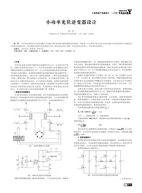
关键词: 光伏发电;逆变器;直流升压中图分类号:TM91 文献标识码:A 文章编号:1671-7597(2011)0120057-010 引言压器的次级线圈串接在一起;整流滤波电路将高压交流电,整流滤波生成高压直流电,整流滤波电路采用全波整流滤波,由四个二极管组成的整流光伏发电是将太阳的光能转化为电能的发电方式,它包括光化学发桥串联电感和电容组成的滤波电路构成;PWM 生成及稳压控制电路主要由电、光感应发电和光伏发电[1-2]。
光伏发电是利用光伏电池板将太阳光意法半导体公司(ST )生产的PWM 控制器SG3525A 来完成[5]。
其中的PWM 生的能量直接转化为电能的发电方式。
由于光伏电池和蓄电池是直流电源,成及稳压控制电路如图2所示。
当负载为交流负载时,就需要逆变器将直流电能转换成交流电能的作用。
推挽升压电路中的四个开关器件(Q5、Q6、Q7、Q8)在高频开关信号光伏逆变装置从结构上一般可分为工频和高频两种,工频光伏逆变装置由下工作,并且两个为一组在PWM 信号控制下交替导通。
PWM 控制器用简单的于带有工频变压器,所以体积较大且比较笨重,更主要的是效率较低。
随比例控制方法动态地调节PWM 输出信号的脉宽,当直流电压高于标准值着电力电子元器件的逐步发展,对于功率较小的系统,高频光伏逆变装置时,脉宽占空比为10%,当直流电压低于标准值时脉宽占空比为50%,升压已经得到了广泛的使用,高频光伏逆变装置一般是用DC-DC 高频升压电路电路能够很快的稳定在给定的参考电压上。

微型光伏逆变器设计要素及拓扑结构1.微型逆变器设计要素与整个系统使用一个逆变器相比,为系统内每个太阳能电池组件都配备一个微型逆变器会再次提升整个系统的转换效率。
微型逆变器拓扑的主要好处是,即便其中一个逆变器消失故障,能量转换仍能进行。
设计微型逆变器需要考虑的要素如下:1)变换效率高。
并网逆变器的变换效率直接影响整个发电系统的效率,为了保证整个系统较高的发电效率,要求并网微型逆变器具有较高的变换效率。
2)牢靠性高。
由于微型逆变器直接与太阳能电池组件集成,一般与太阳能电池组件一起放于室外,其工作环境恶劣,要求微型逆变器具有较高的牢靠性3)寿命长。
太阳能电池组件的寿命一般为二十年,微型逆变器的使用寿命应当与太阳能电池组件的寿命相当。
4)体积小。
微型逆变器直接与太阳能电池组件集成在一起,其体积越小越简单与太阳能电池组件集成。
5)成本低。
低成本是产品进展的必定趋势,也是微型逆变器市场化的需求。
认真权衡这些高层次要求是确定MCU需要哪些功能的最好方法,例如,当并联太阳能电池组件时需要负载平衡掌握。
所选MCU 必需能检测负载电流以及能通过开/关掌握MOSFET上升或降低输出电压,这需要一个高速片上ADC来采样电压和电流。
对于针对光伏逆变器应用所设计的MCU,一个极具价值的特性是双片上振荡器,可用于时钟故障检测以提高牢靠性。
能够同时运行两个系统时钟的力量也有助于削减太阳能电池组件安装时消失的问题。
由于在微型逆变器设计中分散了如此多的创新,对MCU来说,其最重要的特性或许就是软件编程力量,该特性使得在电源电路设计和掌握中拥有最高的敏捷性。
片上集成恰当的掌握外设以及高模拟集成度是保证系统低成本的两个基本要素,为执行针对优化转换、系统监控和能量存储各环节中的效率所开发出的算法,高性能也是必需的。
2.微型逆变器拓扑结构微型逆变器的特别应用需求,打算了其不能采纳传统的降压型逆变器拓扑结构,如全桥、半桥等拓扑,而应当选择能够同时实现升降压变换功能的变换器拓扑,除能够实现升降压变换功能外,还应实现电气隔离;另一方面,高效率、小体积的要求打算了其不能采纳工频变压器实现电气隔离,需要采纳高频变压器。
适用于微网运行的太阳能微逆变器设计下载温馨提示:该文档是我店铺精心编制而成,希望大家下载以后,能够帮助大家解决实际的问题。
文档下载后可定制随意修改,请根据实际需要进行相应的调整和使用,谢谢!本店铺为大家提供各种各样类型的实用资料,如教育随笔、日记赏析、句子摘抄、古诗大全、经典美文、话题作文、工作总结、词语解析、文案摘录、其他资料等等,如想了解不同资料格式和写法,敬请关注!Download tips: This document is carefully compiled by the editor. I hope that after you download them, they can help you solve practical problems. The document can be customized and modified after downloading, please adjust and use it according to actual needs, thank you!In addition, our shop provides you with various types of practical materials, such as educational essays, diary appreciation, sentence excerpts, ancient poems, classic articles, topic composition, work summary, word parsing, copy excerpts, other materials and so on, want to know different data formats and writing methods, please pay attention!太阳能微逆变器是一种能够将太阳能光伏板产生的直流电转换为交流电的装置,是针对小规模太阳能发电系统的设计,能够将太阳能转换为电能并接入微网系统中。
1KW光伏发电单相离网220V 逆变器设计毕业设计目录1 绪论 (3)1.1太阳能应用的背景 (3)1.2光伏发电应用现状和意义 (2)1.2.1 国内光伏发电应用现状 (2)1.2.2 国外光伏发电发展现状 (3)1.2.3 研究的意义 (4)1.3本课题研究的内容 (4)1.4本课题结构 (4)2 光伏发电系统的基本组成和工作方式 (5)2.1光伏发电系统的基本组成 (5)2.2光伏发电系统的工作方式 (6)3 太阳能电池和MPPT控制 (9)3.1太阳能电池的工作原理 (9)3.1.1 太阳能电池的V-I特性 (10)3.1.2 太阳能电池最大效率点的跟踪控制(MPPT) (13)3.1.3 常用MPPT控制技术 (14)3.2光伏组件的几种结构 (17)4 蓄电池的分类和充电方式 (19)4.1蓄电池的分类 (19)4.2蓄电池的充电方式 (20)5 主电路拓扑、控制方式及IPM模块的介绍 (23)5.1DC-DC部分的电路拓扑 (23)5.2DC-AC(逆变)部分的电路拓扑 (24)5.3控制方式 (25)5.4IPM模块的介绍 (27)6 本课题中蓄电池以及光伏电池的选择 (30)6.1蓄电池的选择 (30)6.2光伏电池的选择 (31)7 1KW单相离网220V逆变器的硬件系统设计 (32)7.1系统的构成和主要参数 (32)7.1.1 系统的构成 (32)7.1.2 主要参数 (32)7.2主电路拓扑及电路主要参数设计 (33)7.2.1 主电路拓扑 (33)7.2.2 功率开光管的选择 (33)7.2.3 功率开光管的缓冲电路的设计 (34)7.2.4 电路主要参数设计 (34)7.3IPM模块PM50B4LB060的驱动电源和外围的保护 (36)7.3.1 PM50B4LB060驱动电路 (38)7.3.2 PM50B4LB060外围的保护 (40)7.4基于DSP的控制系统设计 (40)7.4.1 DSP端口资源的分配 (42)7.4.2 取样检测电路 (43)8 系统软件的构架 (46)8.1系统的软件构架 (46)8.1.1 PI算法的程序框图 (48)8.1.2 PI控制程序框图 (49)8.1.3 SPWM波的生成 (50)8.1.4 系统的保护 (52)9 结论与展望 (53)9.1结论 (53)9.2展望 (53)参考文献 (54)翻译部分 (56)英文原文 (56)中文翻译 (60)致谢 (70)1 绪论1.1 太阳能应用的背景目前,世界能源结构中,人类主要利用的是化石能源,其中石油、天然气、煤炭的消费构成分别为41%、23%和27%而根据目前所探明的储量和消费量计算,这些能源资料仅可供全世界大约消费170年。
Microchip连接电网的太阳能微逆变器220V参考设计公司的衔接电网的太阳能微参考设计(220V)采纳ds33FJx6GS系列产品.该16位数字信号控制器包括功能和高性能16位微控制器()架构,3.0V-3.6V时的性能高达40.太阳能微逆变器系数的峰值效率高达94%,输出的THD小于5%,功率因素大于0.95,具有最大功率点跟踪(MPPT),全数字控制,太阳能电池板的从25V到55VDC,MPPT电压25V-45V,最大DC短路电流10A,广泛用于衔接电网农村家庭太阳能系统.本文介绍了dsPIC33FJx6GS系列主要特性,方框图,CPU核方框图,太阳能微逆变器参考设计框图,和材料清单与布局图.dsPIC33FJ06GS101/X02 and dsPIC33FJ16GSX02/X04 devices contain extensive Digital Signal Processor (DSP) functionality with a high-performance, 16-bit microcontroller (MCU) architecture.dsPIC33FJx6GS系列主要特性:Operating Range: Up to 40 MIPS Operation (at 3.0-3.6V):- Industrial temperature range (-40℃ to +85℃)- Extended temperature range (-40℃ to +125℃)High-Performance DSC CPU:Modified Harvard ArchitectureC Compiler Optimized Instruction Set16-Bit Wide Data Path24-Bit Wide InstructionsProgram Memory Addressing up to 4M Instruction WordsLinear Data Memory Addressing up to 64 Kbytes83 Base Instructions: Mostly 1 Word/1 CycleTwo 40-Bit Accumulators with Rounding and Saturation Options Flexible and Powerful Addressing modes:- Indirect- Modulo- Bit-ReversedSoftware Stack16 x 16 Fractional/Integer Multiply Operations 32/16 and 16/16 Divide OperationsSingle-Cycle Multiply and Accumulate:- Accumulator write back for DSP operations- Dual data fetchUp to ±16-Bit Shifts for up to 40-Bit Data Digital I/O:Peripheral Pin Select FunctionalityUp to 35 Programmable Digital I/O PinsWake-up/Interrupt-on-Change for up to 30 Pins Output Pins can Drive Voltage from 3.0V to 3.6V Up to 5V Output with Open-Drain Configuration 5V Tolerant Digital Input Pins (except RB5) 16 mA Source/Sink on All pinsOn-Chip Flash and SRAM:Flash Program Memory (up to 16 Kbytes)Data SRAM (up to 2 Kbytes)Boot and General Security for Program Flash Peripheral Features:Timer/Counters, up to Three 16-Bit Timers:- Can pair up to make one 32-bit timerInput Capture (up to two channels):- Capture on up, down or both edges- 16-bit capture input functions- 4-deep FIFO on each captureOutput Compare (up to two channels):- Single or Dual 16-Bit Compare mode- 16-Bit Glitchless PWM mode4-Wire SPI:- Framing supports I/O interface to simple codecs- 1-deep FIFO Buffer.- Supports 8-bit and 16-bit data- Supports all serial clock formats and sampling modes I2C :- Supports Full Multi-Master Slave mode- 7-bit and 10-bit addressing- Bus collision detection and arbitration- Integrated signal conditioning- Slave address masking UART:- Interrupt on address bit detect- Interrupt on UART error- Wake-up on Start bit from Sleep mode - 4-character TX and RX FIFO buffers- LIN bus support- IrDA encoding and decoding in hardware - High-Speed Baud mode- Hardware Flow Control with CTS and RTS Interrupt Controller:5-Cycle LatencyUp to 35 Available Interrupt SourcesUp to Three External InterruptsSeven Programmable Priority LevelsFour Processor ExceptionsHigh-Speed PWM Module Features:Up to Four PWM Generators with Four to Eight Outputs Individual Time Base and Duty Cycle for each of the Eight PWM OutputsDead Time for Rising and Falling EdgesDuty Cycle Resolution of 1.04 nsDead-Time Resolution of 1.04 nsPhase Shift Resolution of 1.04 nsFrequency Resolution of 1.04 nsPWM modes Supported:- Standard Edge-Aligned- True Independent Output- Complementary - Center-Aligned- Push-Pull- Multi-Phase- Variable Phase- Fixed Off-Time- Current Reset- Current-LimitIndependent Fault/Current-Limit Inputs for 8 PWM Outputs Output Override ControlSpecial Event TriggerPWM Capture FeaturePrescaler for Input ClockDual Trigger from PWM toPWMxL, PWMxH Output Pin SwappingPWM4H, PWM4L Pins RemappableOn-the-Fly PWM Frequency, Duty Cycle and Phase Shift Changes Disabling of Individual PWM GeneratorsLeading-Edge Blanking (LEB) Functionality High-Speed Analog ComparatorUp to Four Analog Comparators:- 20 ns response time- 10-bit for each analog comparator- DACOUT pin to provide DAC output- Programmable output polarity- Selectable input source- ADC sample and convert capabilityPWM Module Interface:- PWM duty cycle control - PWM period control- PWM Fault detect High-Speed 10-Bit ADC10-Bit ResolutionUp to 12 Input Channels Grouped into Six Conversion Pairs Two Internal Reference Monitoring Inputs Grouped into a Pair Successive Approximation Register (SAR) Converters for Parallel Conversions of Analog Pairs:- 4 Msps for devices with two SARs- 2 Msps for devices with one SARDedicated Result Buffer for each Analog ChannelIndependent Trigger Source Section for each Analog Input Conversion PairPower Management:On-Chip 2.5V Voltage RegulatorSwitch between Clock Sources in Real TimeIdle, Sleep, and Doze modes with Fast Wake-upFlash Technology:Low-Power, High-Speed Flash TechnologyFully Static Design3.3V (±10%) Operating VoltageIndustrial and Extended TemperatureLow-Power ConsumptionSystem Management:Flexible Clock Options:- External, crystal, resonator, internal RC- Phase-Locked Loop (PLL) with 120 MHz VCO- Primary Crystal Oscillator (OSC) in the range of 3 MHz to 40 MHz - Internal Low-Power RC (LPRC) oscillator at a frequency of 32 kHz- Internal Fast RC (FRC) oscillator at a frequency of 7.37 MHz Power-on Reset (POR)Brown-out Reset (BOR)Power-up Timer (PWRT)Oscillator Start-up Timer (OST)Watchdog Timer with its RC OscillatorFail-Safe Clock Monitor (FSCM)Reset by Multiple SourcesIn-Circuit Serial Programming (ICSP )Reference Oscillator OutputApplication ExamplesAC-to-DC ConvertersAutomotive HIDBattery ChargersDC-to-DC ConvertersDigital LightingInduction CookingBallastRenewable Power/Pure Sine Wave Inverters Uninterruptible Power Supply (UPS) Packaging: 18-Pin SOIC28-Pin SPDIP/SOIC/QFN-S44-Pin TQFP/QFN。
Microchip连接电网的太阳能微逆变器220V参考设计Microchip公司的连接电网的太阳能微逆变器参考设计(220V)采用dsPIC33FJx6GS系列产品.该16位数字信号控制器包括DSP功能和高性能16位微控制器(MCU)架构,3.0V-3.6V时的性能高达40MIPS.太阳能微逆变器系数的峰值效率高达94%,输出电流的THD小于5%,功率因素大于0.95,具有最大功率点跟踪(MPPT),全数字控制,太阳能电池板的电压从25V到55VDC,MPPT电压25V-45V,最大DC短路电流10A,广泛用于连接电网农村家庭太阳能系统.本文介绍了dsPIC33FJx6GS系列主要特性,方框图,CPU核方框图,太阳能微逆变器参考设计框图,电路图和材料清单与PCB布局图.dsPIC33FJ06GS101/X02 and dsPIC33FJ16GSX02/X04 devices contain extensive Digital Signal Processor (DSP) functionality with a high-performance, 16-bit microcontroller (MCU) architecture.dsPIC33FJx6GS系列主要特性:Operating Range:• Up to 40 MIPS Operation (at 3.0-3.6V):- Industrial temperature range (-40℃ to +85℃)- Extended temperature range (-40℃ to +125℃)High-Performance DSC CPU:• Modified Harvard Architecture• C Compiler Optimized Instruction Set• 16-Bit Wide Data Path• 24-Bit Wide Instructions• Linear Program Memory Addressing up to 4M Instruction Words• Linear Data Memory Addressing up to 64 Kbytes• 83 Base Instructions: Mostly 1 Word/1 Cycle• Two 40-Bit Accumulators with Rounding and Saturation Options• Flexible and Powerful Addressing modes:- Indirect- Modulo- Bit-Reversed• Software Stack• 16 x 16 Fractional/Integer Multiply Operations• 32/16 and 16/16 Divide Operations• Single-Cycle Multiply and Accumulate:- Accumulator write back for DSP operations- Dual data fetch• Up to ±16-Bit Shifts for up to 40-Bit DataDigital I/O:• Peripheral Pin Select Functionality• Up to 35 Programmable Digital I/O Pins• Wake-up/Interrupt-on-Change for up to 30 Pins• Output Pins can Drive Voltage from 3.0V to 3.6V• Up to 5V Output with Open-Drain Configuration• 5V Tolerant Digital Input Pins (except RB5)• 16 mA Source/Sink on All PWM pinsOn-Chip Flash and SRAM:• Flash Program Memory (up to 16 Kbytes)• Data SRAM (up to 2 Kbytes)• Boot and General Security for Program FlashPeripheral Features:• Timer/Counters, up to Three 16-Bit Timers:- Can pair up to make one 32-bit timer• Input Capture (up to two channels):- Capture on up, down or both edges- 16-bit capture input functions- 4-deep FIFO on each capture• Output Compare (up to two channels):- Single or Dual 16-Bit Compare mode- 16-Bit Glitchless PWM mode• 4-Wire SPI:- Framing supports I/O interface to simple codecs- 1-deep FIFO Buffer.- Supports 8-bit and 16-bit data- Supports all serial clock formats and sampling modes• I2C™:- Supports Full Multi-Master Slave mode- 7-bit and 10-bit addressing- Bus collision detection and arbitration- Integrated signal conditioning- Slave address masking• UART:- Interrupt on address bit detect- Interrupt on UART error- Wake-up on Start bit from Sleep mode- 4-character TX and RX FIFO buffers- LIN bus support- IrDA® encoding and decoding in hardware- High-Speed Baud mode- Hardware Flow Control with CTS and RTSInterrupt Controller:• 5-Cycle Latency• Up to 35 Available Interrupt Sources• Up to Three External Interrupts• Seven Programmable Priority Levels• Four Processor ExceptionsHigh-Speed PWM Module Features:• Up to Four PWM Generators with Four to Eight Outputs• Individual Time Base and DutyCycle for each of the Eight PWM Outputs• Dead Time for Rising and Falling Edges• Duty Cycle Resolution of 1.04 ns• Dead-Time Resolution of 1.04 ns• Phase Shift Resolution of 1.04 ns• Frequency Resolution of 1.04 ns• PWM modes Supported:- Standard Edge-Aligned- True Independent Output- Complementary- Center-Aligned- Push-Pull- Multi-Phase- Variable Phase- Fixed Off-Time- Current Reset- Current-Limit• Independent Fault/Current-Limit Inputs for 8 PWM Outputs• Output Override Control• Special Event Trigger• PWM Capture Feature• Prescaler for Input Clock• Dual Trigger from PWM to ADC• PWMxL, PWMxH Output Pin Swapping• PWM4H, PWM4L Pins Remappable• On-the-Fly PWM Frequency, Duty Cycle and Phase Shift Changes• Disabling of Individual PWM Generators• Leading-Edge Blanking (LEB) Functionality High-Speed Analog Comparator• Up to Four Analog Comparators:- 20 ns response time- 10-bit DAC for each analog comparator- DACOUT pin to provide DAC output- Programmable output polarity- Selectable input source- ADC sample and convert capability• PWM Module Interface:- PWM duty cycle control- PWM period control- PWM Fault detect High-Speed 10-Bit ADC• 10-Bit Resolution• Up to 12 Input Channels Grouped into Six Conversion Pairs• Two Internal Reference Monitoring Inputs Grouped into a Pair• Successive Approximation Register (SAR) Converters for Parallel Conversions of Analog Pairs:- 4 Msps for devices with two SARs- 2 Msps for devices with one SAR• Dedicated Result Buffer for each Analog Channel• Independent Trigger Source Section for each Analog Input Conversion PairPower Management:• On-Chip 2.5V Voltage Regulator• Switch between Clock Sources in Real Time• Idle, Sleep, and Doze modes with Fast Wake-upCMOS Flash Technology:• Low-Power, High-Speed Flash Technology• Fully Static Design• 3.3V (±10%) Operating Voltage• Industrial and Extended Temperature• Low-Power ConsumptionSystem Management:• Flexible Clock Options:- External, crystal, resonator, internal RC- Phase-Locked Loop (PLL) with 120 MHz VCO- Primary Crystal Oscillator (OSC) in the range of 3 MHz to 40 MHz- Internal Low-Power RC (LPRC) oscillator at a frequency of 32 kHz- Internal Fast RC (FRC) oscillator at a frequency of 7.37 MHz• Power-on Reset (POR)• Brown-out Reset (BOR)• Power-up Timer (PWRT)• Oscillator Start-up Timer (OST)• Watchdog Timer with its RC Oscillator• Fail-Safe Clock Monitor (FSCM)• Reset by Multiple Sources• In-Circuit Serial Programming™ (ICSP™)• Reference Oscillator OutputApplication Examples• AC-to-DC Converters• Automotive HID• Battery Chargers• DC-to-DC Converters• Digital Lighting• Induction Cooking• LED Ballast• Renewable Power/Pure Sine Wave Inverters• Uninterruptible Power Supply (UPS) Packaging:• 18-Pin SOIC• 28-Pin SPDIP/SOIC/QFN-S• 44-Pin TQFP/QFN图 1.dsPIC33FJx6GS系列方框图图2.dsPIC33FJx6GS系列CPU核方框图图3.采用dsPIC33FJ16GS504的PFC 和三输出(12V,5V 和3.3V)AC/DC电源框图太阳能(光伏(PV))微逆变器参考设计Due to global environmental concerns, photovoltaic (PV) systems (i.e., solar panels) are becoming more common as a renewable energy source.The main drawbacks of PV energy are the high cost of manufacturing silicon solar panels and the low conversion efficiency. However, with the latest techniques in manufacturing, PV systems are becoming more efficient, aswell as cost effective.The conversion of the output voltage from a solar panel into usable DC or AC voltage must be done at its Maximum Power Point, or MPP. MPP is the PV output voltage at which the PV module delivers maximum energy to load.Interfacing a solar inverter module with the power grid involves two major tasks. One is to ensure that the solar inverter module is operated at the Maximum Power Point (MPP). The second is to inject a sinusoidal current into the grid. Since the inverter is connected to the grid, the standards given by the utility companies must be obeyed. The EN61000-3-2, IEEE1547 standards, and the U.S. National Electrical Code (NEC) 690, are worth considering. These standards deal with issues like power quality, detection of islanding operation, grounding, and so on.These inverters must be able to detect an islanding situation, and take appropriate action in order to prevent bodily harm and damage to equipment connected to the grid. Islanding is the continued operation of the inverter when the grid has been removed intentionally, by accident, or by damage. In other words, if the grid has been removed from the inverter; the inverter should then stop supplying power to the grid or energizing the grid.The most common solar technologies today are the monocrystalline and multi-crystalline silicon modules.The MPP voltage range for these PV modules is normally defined in the range from 27V to 45V, at a power generation of approximate 200W, and their open-circuit voltage is below 45V.In order to capture the maximum energy from the PV module, solar inverters must guarantee that the PV module is operated at the MPP. This is accomplished by the maximum power point control loop known as the Maximum Power Point Tracker (MPPT). It also involves PV output voltage ripple at the terminals of the PV module being sufficiently small, in order to operate around the MPP without too much variation in PV Current.图3.农村家庭太阳能系统框图图4.模块化逆变器(微逆变器)系统框图图5.太阳能微逆变器系统两级拓扑图图 6.太阳能微逆变器参考设计框图图7.交错式反激转换器电路图8.连接电网的太阳能微逆变器框图图9.连接电网的太阳能微逆变器参考设计板外形图This reference design demonstrates the flexibility and power of SMPS dsPIC® Digital Signal Controllers in Grid connected power conversion systems. This reference design works with any photovoltaic (PV) panel of maximum 220 Watts having open circuit voltage between 25V to 55V DC. This reference design ensures maximum power tracking for PV panel voltage between 25V to 45V DC. Two versions of this reference design is available to support 110V and 220V Grid.This reference design is implemented using a single dsPIC33F “GS” digital-power DSCs from Microchip that provides the full digital control of the power conversion and system management functions. As shown in this reference design the dsPIC33F ‘GS’ devices enable designers to easily and cost effectively create products using advanced switching techniques that lower switching losses and enable efficiencies as high as 94%. Grid-Connected Solar Micro Inverter Reference Design is royalty free when used in accordance with the licensing agreement.太阳能微逆变器参考设计主要特性:Peak efficiency of up to 94%Beta build peak efficiency of up to 92%Output current THD < 5%Power factor >0.95Maximum power point trackingGrid voltage and frequency trackingProtection against various current and voltage faultsSystem Islanding to detect grid failureFull Digital ControlSpecifications:Micro Inverter for individual PV Module up to 220WWide PV Panel voltage : 25V to 55V DCMaximum Power Point Trackingvoltage: 25V to 45VMaximum DC short circuit current : 10AGrid Frequency range :47 – 53 Hz for 220V systems57 – 63 Hz for 110V systemsGrid voltage range :90V – 140V for 110V systems180V – 264V for 220V systems图10.太阳能微逆变器参考设计电路图(1)图11.太阳能微逆变器参考设计电路图(2)图12.太阳能微逆变器参考设计电路图(3)图13.太阳能微逆变器参考设计电路图(4)图15.太阳能微逆变器参考设计电路图(4)图16.太阳能微逆变器参考设计板PCB布局图(顶层)图17.太阳能微逆变器参考设计板PCB布局图(底层)太阳能微逆变器参考设计材料清单见:太阳能微逆变器参考设计(220V)材料清单.xls详情请见:/downloads/en/AppNotes/01338D.pdf。