s_
- 格式:doc
- 大小:22.50 KB
- 文档页数:3

sack/ sæk/ n.袋,麻袋;开除sacrifice/ ‘sækrifais/ n.&vt.牺牲;南祭saddle/ ‘sædl/ n.鞍子,马鞍sail/ seil/ n.帆;船vi.航行sake/ seik/ n.缘故,理由sample/ ‘sa:mpl/ n.样品;实例,标本satellite/ ‘sætəlait/ n.卫星;人造卫星satisfactory/ sætis’fæktəri/ a.令人满意的,良好的saucer/ ‘sɔ:sə/ n.茶托,浅碟sausage/ ‘sɔsidʒ/ n.香肠,腊肠saw/ sɔ:/ n.锯子vt.锯,锯开say/ sei/ vt.比如说[用于举例]scale/ skeil/ n.天平,磅秤,秤scale/ skeil/ n.标度;比例;大小scan/ skæn/ vt.细看;浏览;扫描scarcely/ ‘skeəsli/ ad.仅仅;几乎不scatter/ ‘skætə/ vt.使消散;撒;散播scenery/ ‘si:nəri/ n.舞台布景;风景schedule/ ‘ʃedju:l/ n.时间表;计划表scheme/ ski:m/ n.计划,规划;诡计scholar/ ‘skɔlə/ n.学者(尤指文学方面) scientific/ saiən’tifik/ a.科学(上)的scissors/ ‘sizəz/ n.剪刀,剪子score/ skɔ:/ n.得分,比数,成绩scout/ skaut/ n.侦察员,侦察机scrape/ skreip/ vt.&vi.&n.刮,擦scratch/ skrætʃ/ vt.&vi.&n.搔;抓screw/ skru:/ n.螺旋,螺丝vt.拧紧seal/ ‘si:l/ n.封蜡;印记vt.封seal/ ‘si:l/ n.海豹secondary/ ‘sekəndəri/ a.第二的;次要的secretary/ ‘sekrətri/ n.秘书;书记;大臣section/ ‘sekʃən/ n.切片;一段;部门secure/ si’kjuə/ a.安心的;安全的security/ si’kjuəriti/ n.安全,安全感seed/ si:d/ n.种(子),籽,萌芽seek/ si:k/ vt.寻找,探索;试图seize/ si:z/ vt.抓住,逮捕;夺取semiconductor/ semikən’dΛktə/ n. 半导体senate/ senit/ n.参议院,上院senior/ ‘si:njə/ a.年少的;地位较高的sensible/ ‘sensəbl/ a.感觉得到的;明智的sensitive/ ‘sensitiv/ a.敏感的;灵敏的separate/ ‘sepəreit, ‘sepərit/ a.分离的;个别的sequence/ ‘si:kwəns/ n.连续,继续;次序series/ ‘siəri:z/ n.连续,系列;丛书serve/ sə:v/ vt.为…服务;招待session/ ‘seʃən/ n.会议,一段时间setting/ ‘setiŋ/ n.安装,调整;环境settle/ ‘setl/ vt.安排;安放;调停settlement/ ‘setlmənt/ n.解决;殖民,殖民地severe/ si’viə/ a.严格的;严厉的sew/ səu/ vt.缝制vi.缝纫shade/ ʃeid/ n.荫;遮光物vi.荫蔽shave/ ʃeiv/ vt.剃,刮vi.修面shear/ ʃiə/ vt.剪;剥夺vi.剪shed/ ʃed/ vt.流出;散发;脱落shed/ ʃed/ n.棚,小屋;贷棚sheet/ ʃi:t/ n.被单;纸张;薄板shelf/ ʃelf/ n.搁板,架子shelter/ ‘ʃeltə/ n.隐蔽处;掩蔽,庇护shield/ ʃi:ld/ n.盾;防护物vt.保护shift/ ʃift/ vt.替换,转移n.转换shiver/ ‘ʃivə/ vi.颤抖,哆嗦n.冷颤shoot/ ʃu:t/ vt.发射;射中n.发芽shore/ ʃɔ:/ n.滨,岸shortage/ ‘ʃɔ:tidʒ/ n.不足,缺少,不足额shortly/ ‘ʃɔ:tli/ ad.立刻;简短地shot/ ʃɔt/ n.发射;弹丸;射门shower/ ‘ʃəuə, ‘ʃauə/ n.阵雨;(一)阵;淋浴shriek/ ʃri:k/ vi.尖声喊叫n.尖叫声sideways/ ‘saidweiz/ ad.斜着,斜向一边地sightseeing/ ‘saitsi:iŋ/ n.观光,游览sign/ sain/ n.符号;招牌n.签名signal/ ‘signəl/ n.信号vi.发信号signature/ ‘signitʃə/ n.署名,签字,签名significance/ sig’nifikəns/ n.意义,意味;重要性significant/ sig’nifikənt/ n.有意义的;重要的silence/ ‘sailəns/ n.沉默vt.使沉默silent/ ‘sailənt/ a.沉默的;寂静无声的silk/ silk/ n.蚕丝,丝,丝织品silly/ ‘sili/ a.傻的,愚蠢的silver/ ‘silvə/ n.银;银子;银器similar/ ‘similə/ a.相似的,类似的similarly/ ‘similəli/ ad.类似地,相似地simplicity/ sim’plisiti/ n.简单,简易;朴素simplify/ ‘simplifai/ vt.简化,使单纯simply/ ‘simpli/ ad.简单地;朴素地singular/ ‘siŋgjulə/ a.单一的;非凡的site/ sait/ n.地点,地基;场所sketch/ sketʃ/ n.略图;速写;概略skilled/ skild/ a.有技能的,熟练的skillful/ ‘skilful/ a.灵巧的,娴熟的skim/ skim/ vt.掠过,擦过;略读slam/ slæm/ vt.使劲关,砰地放下sleeve/ sli:v/ n.袖子,袖套slender/ ‘slendə/ a.细长的;微薄的slice/ slais/ n.薄片,切片;部分slide/ slaid/ vi.滑vt.使滑动n.滑slippery/ ‘slipəri/ a.滑的,使人滑跤的slit/ slit/ n.裂缝vt.切开,撕开slope/ sləup/ n.倾斜;斜面vi.倾斜smart/ sma:t/ a.巧妙的;洒脱的soak/ səuk/ vt.浸,泡vi.浸泡sɔil/ sɔil/ vt.弄脏vi.变脏solar/ ‘səulə/ a.太阳的,日光的sole/ səul/ n.脚底,鞋底,袜底sole/ səul/ a.单独的,唯一的solemn/ ‘sɔləm/ a.庄严的;隆重的solid/ ‘sɔlid/ a.固体的n.固体soluble/ ‘sɔljubl/ a.可溶的;可以解决的solution/ sə’lju:ʃən/ n.解决,解答;溶解solve/ ‘sɔlv/ vt.解答,解释,解决somebody/ ‘sΛmbədi/ pron.某人,有人somehow/ ‘sΛmhau/ ad.由于某种原因sometime/ ‘sΛmtaim/ ad.在某一时候;从前somewhat/ ‘sΛmwɔt/ pron.一点儿ad.有点sophisticated/ sə’fistikeitid/ a.老于世故的;高级的sore/ sɔ:/ a.痛的;恼火的n.疮sorrow/ ‘sɔrəu/ n.悲痛,悲哀,悲伤sort/ sɔ:t/ n.种类;类别vt.整理sound/ saund/ a.健康的;完好的sour/ ‘sauə/ a.酸的;脾气坏的sow/ səu/ vt.播(种) vi.播种spacecraft/ ‘speiskra:ft/ n.航天器,宇宙飞船spade/ speid/ n.铲,铁锹span/ spæn/ n.跨距;一段时间spare/ speə/ vt.节约 a.多余的spark/ spa:k/ n.火花,火星specialist/ speʃəlist/ n.专家specialize/ ‘speʃəlaiz/ vi.成为…专家;专攻specify/ ‘spesifai/ vi.指定,详细说明specimen/ ‘spesimin/ n.样本,标本,样品sphere/ sfiə/ n.球,圆体;范围spill/ spil/ vt.使溢出vi.溢出spin/ spin/ vt.纺;使旋转n.旋转spite/ spait/ n. 恶意,怨恨,不顾vt. 刁难,欺侮split/ split/ vt.劈开vi.被劈开spɔil/ spɔil/ vt.损坏,糟蹋;宠坏sponsor/ ‘spɔnsə/ n.发起者vt.发起sportsman/ ‘spɔ:tsmən/ n.运动员spray/ sprei/ n.浪花;喷雾vt.喷spring/ spriŋ/ vi.跳,跃n.跳跃;泉spur/ spə:/ n.刺激物vt.刺激square/ skweə/ n.正方形;广场squeeze/ ‘skwi:z/ vt.&vi.榨,挤;压榨stability/ stə’biliti/ n.稳定,稳定性,巩固stable/ ‘steibl/ a.稳定的,不变的stable/ ‘steibl/ n.厩,马厩,牛棚stack/ stæk/ n.堆,垛vt.堆积staff/ sta:f/ n.工作人员;参谋stage/ steidʒ/ n.舞台;戏剧;阶段stain/ stein/ vt.沾污;给…着色stair/ steə/ n.楼梯stake/ steik/ n.桩;赌金;奖品stale/ steil/ n.陈腐的;走了气的static/ ‘stætikl/ a.静的;静态的statistical/ stə’tistikl/ a.统计的,统计学的statue/ ‘stætju:/ n.塑像,雕像,铸像status/ ‘steitəs/ n.地位,身分steady/ ‘stedi/ a.稳固的vt.使稳定steam/ sti:m/ n.蒸汽vi.蒸发vt.蒸steamer/ ‘sti:mə/ n.轮船,汽船steel/ ‘sti:l/ n.钢,钢铁steep/ sti:p/ a.险峻的,陡峭的steer/ stiə/ vt.&vi.驾驶stem/ stem/ n.茎,(树)干vi.起源sticky/ ‘stiki/ a.粘性的;胶粘的stiff/ stif/ a.硬的;僵直的stimulate/ ‘stimjuleit/ vt.刺激,激励,激发sting/ stiŋ/ vt.刺;刺痛vi.&n.刺stir/ stə:/ vt.动;拨动;激动stock/ stɔk/ n.原料;库存品;股本stocking/ ‘stɔkiŋ/ n.长(统)袜stoop/ stu:p/ vi.俯身;弯身n.弯腰storage/ ‘stɔ:ridʒ/ n.贮藏;贮藏量store/ stɔ:/ n.贮藏;贮存品;商店storey/ ‘stɔ:ri/ n.(层)楼stove/ stəuv/ n.炉,火炉,电炉strain/ ‘strein/ vt.拉紧vi.尽力strange/ streindʒ/ a.陌生的;奇怪的stranger/ ‘streindʒə/ n.陌生人;新来者strap/ stræp/ n.带子vt.捆扎strategy/ ‘strætidʒi/ n.战略;策略straw/ strɔ:/ n.稻草,麦杆吸管strengthen/ ‘streŋθən/ vt.加强,巩固stress/ stres/ n.压力;重音vt.着重stretch/ stretʃ/ vt.伸展vi.伸n.伸展string/ striŋ/ n.线,细绳;一串strip/ strip/ vt.剥;夺去n.条带stripe/ straip/ n.条纹,条子stroke/ strəuk/ n.打,击;鸣声;中风stroke/ strəuk/ vt.&n.抚,摩,捋structural/ ‘strΛktʃərəl/ a.结构的,构造的stuff/ stΛf/ n.材料vt.装,填,塞submarine/ ‘sΛbməri:n/ a.水下的n.潜水艇submerge/ sΛb’mə:dʒ/ vt.浸没vi.潜入水中submit/ sΛb’mit/ vt.使服从vi.服从subsequent/ ‘sΛbsikwənt/ a.随后的,后来的substance/ ‘sΛbstəns/ n.物质;实质;本旨substantial/ səb’stænʃəl/ a.物质的;坚固的substitute/ ‘sΛbstitju:t/ n.代替人vt.用…代替subtract/ səb’trækt/ vt.减,减去,去掉subway/ ‘sΛbwei/ n.地道;地下铁路succession/ sək’seʃən/ n.连续;继任,继承successive/ sək’sesiv/ a.连续的;接连的suck/ sΛk/ vt.吸,吮,啜;吸收sufficient/ sə’fiʃənt/ a.足够的,充分的suit/ sju:t/ n.起拆,诉讼【其动词形式为sue】vt.适合sulfur/ ‘sΛlfə/ n.硫(磺),硫黄sulphur/ ‘sΛlfə/ n.硫(磺),硫黄sum/ sΛm/ n.总数;金额vi.共计summarize/ ‘sΛməraiz/ vt.概括,概述,总结superficial/ sju:pə’fiʃəl/ a.表面的;肤浅的superior/ sju:’piəriə/ a.较高的;优越的supplement/ ‘sΛplimənt/ n.&vt.增补,补充suppose/ sə’pəuz/ vt.猜想;假定;让supreme/ sju:’pri:m/ a.最高的;最大的surgery/ ‘sə:dʒəri/ n.外科,外科手术surrender/ sə’rendə/ vt.交出vi.投降surroundings/ sə’raundiŋz/ n.周围的事物,环境survey/ sə:’vei/ vt.俯瞰;检查;测量survive/ sə’vaiv/ vt.幸免于vi.活下来suspect/ səs’pekt, ‘sΛspekt/ vt.怀疑vi.疑心suspend/ səs’pend/ vt.吊,悬;推迟suspicion/ səs’piʃən/ n.怀疑,疑心,猜疑suspicious / səs’piʃəs/ adj.怀疑的;可疑的sustain/ səs’tein/ vt.支撑;供养;忍受swallow/ ‘swɔləu/ n.燕子swallow/ ‘swɔləu/ vt.&vi.吞下,咽下sway/ swei/ vi.摇动vt.摇;摇动swear/ sweə/ vt.宣(誓) vi.诅咒sweater/ ‘swetə/ n.厚运动衫,毛线衫sweep/ swi:p/ vt.扫;刮起;扫过swell/ swel/ vi.膨胀;隆起;增长swift/ swift/ a.快的;反应快的swing/ swiŋ/ vi.摇摆;回转n.摇摆switch/ switʃ/ n.开关;转换vt.转换sword/ sɔ:d/ n.剑,刀symbol/ ‘simbəl/ n.象征;符号,记号sympathetic/ simpə’θetik/ a.同情的;和谐的sympathize/ ‘simpəθaiz/ vi.同情;同感,共鸣synthetic/ sin’θetik/ a.综合的;合成的systematic(al)/ sisti’mætik(əl)/ a.有系统的;有计划的。
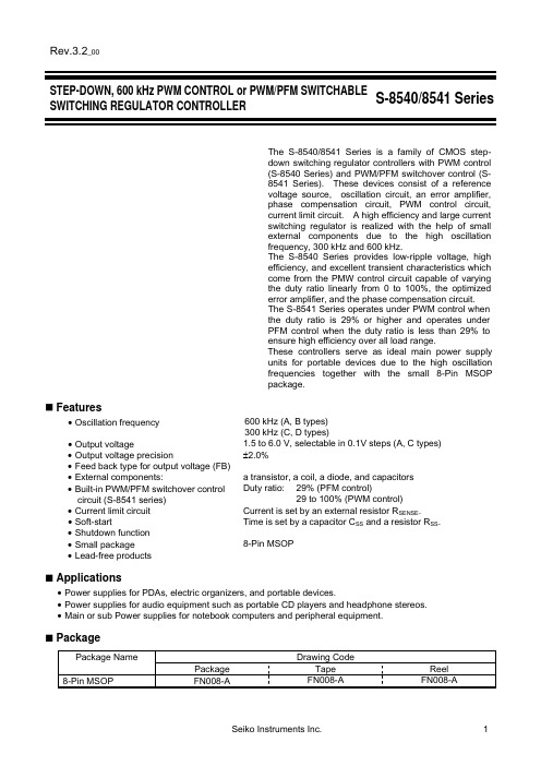
Rev.3.2_00STEP-DOWN, 600 kHz PWM CONTROL or PWM/PFM SWITCHABLE SWITCHING REGULATOR CONTROLLERS-8540/8541 SeriesSeiko Instruments Inc. 1The S-8540/8541 Series is a family of CMOS step-down switching regulator controllers with PWM control (S-8540 Series) and PWM/PFM switchover control (S-8541 Series). These devices consist of a reference voltage source, oscillation circuit, an error amplifier, phase compensation circuit, PWM control circuit, current limit circuit. A high efficiency and large current switching regulator is realized with the help of small external components due to the high oscillation frequency, 300 kHz and 600 kHz.The S-8540 Series provides low-ripple voltage, high efficiency, and excellent transient characteristics which come from the PMW control circuit capable of varying the duty ratio linearly from 0 to 100%, the optimized error amplifier, and the phase compensation circuit. The S-8541 Series operates under PWM control when the duty ratio is 29% or higher and operates under PFM control when the duty ratio is less than 29% to ensure high efficiency over all load range.These controllers serve as ideal main power supply units for portable devices due to the high oscillation frequencies together with the small 8-Pin MSOP package.Features• Oscillation frequency600 kHz (A, B types) 300 kHz (C, D types)• Output voltage1.5 to 6.0 V, selectable in 0.1V steps (A, C types) • Output voltage precision±2.0%• Feed back type for output voltage (FB) • External components:a transistor, a coil, a diode, and capacitors • Built-in PWM/PFM switchover control circuit (S-8541 series) Duty ratio: 29% (PFM control)29 to 100% (PWM control)• Current limit circuit Current is set by an external resistor R SENSE . • Soft-startTime is set by a capacitor C SS and a resistor R SS . • Shutdown function• Small package 8-Pin MSOP • Lead-free productsApplications• Power supplies for PDAs, electric organizers, and portable devices.• Power supplies for audio equipment such as portable CD players and headphone stereos. • Main or sub Power supplies for notebook computers and peripheral equipment.PackagePackage Name Drawing CodePackage Tape Reel8-Pin MSOP FN008-AFN008-A FN008-ASTEP-DOWN, 600 kHz PWM CONTROL or PWM/PFM SWITCHABLE SWITCHING REGULATOR CONTROLLERS-8540/8541 Series Rev.3.2_00Block Diagrams1. A, C types (fixed output voltage)S SFigure 12. B, D types (feed back)S SFigure 22 Seiko Instruments Inc.STEP-DOWN, 600 kHz PWM CONTROL or PWM/PFM SWITCHABLE SWITCHING REGULATOR CONTROLLER Rev.3.2_00 S-8540/8541 SeriesSeiko Instruments Inc. 3Product Name Structure• The control types, product types, and output voltage for the S-8540/8541 series can be selected at theuser’s request. Please refer to the “1. Product name ” for the definition of the product name and “2. Product Name List ” for the full product names. 1. Product nameS -854X X XX FN - XXX T2 GProduct typeA: Fixed output voltage, fosc = 600 kHz B: Feed back type, fosc = 600kHz C: Fixed output voltage, fosc = 300 kHz D: Feed back type, fosc = 300 kHz Output voltage *3 15 to 60(e.g. When the output voltage is 1.5 V, it is expressed as 15.) Control system0: PWM control1: PWM/PFM switching controlFN: 8-Pin MSOPProduct code *2IC direction in tape specifications*1*1. Refer to the taping specifications at the end of this book. *2. Refer to the “2. Product name list ”. *3. 00: Feed back typeSTEP-DOWN, 600 kHz PWM CONTROL or PWM/PFM SWITCHABLE SWITCHING REGULATOR CONTROLLERS-8540/8541 SeriesRev.3.2_00 4 Seiko Instruments Inc.2.Product name list2.1 A, B types (oscillation frequency: 600 kHz)Table 1Output Voltage (V)S-8540XXXFN SeriesS-8541XXXFN Series1.5 S-8540A15FN-IAAT2G − 1.6 −S-8541A16FN-IGBT2G 1.8 S-8540A18FN-IADT2G S-8541A18FN-IGDT2G 2.5 S-8540A25FN-IAKT2G S-8541A25FN-IGKT2G 3.3 S-8540A33FN-IAST2G S-8541A33FN-IGST2G 5.0 S-8540A50FN-IBBT2G −Feed back (1.5 to 6.0) S-8540B00FN-IMAT2G S-8541B00FN-IMDT2G Remark Please consult the SII marketing department for products with an output voltageother than those specified above. 2.2 C,D types (oscillation frequency: 300 kHz)Table 2Output Voltage (V) S-8540XXXFN Series S-8541XXXFN Series1.8 S-8540C18FN-ICDT2G S-8541C18FN-IIDT2G2.5 S-8540C25FN-ICKT2G S-8541C25FN-IIKT2G3.2 −S-8541C32FN-IIRT2G 3.3 S-8540C33FN-ICST2G S-8541C33FN-IIST2GFeed back (1.5 to 6.0) S-8540D00FN-IMBT2G S-8541D00FN-IMET2G Remark Please consult the SII marketing department for products with an output voltageother than those specified above.STEP-DOWN, 600 kHz PWM CONTROL or PWM/PFM SWITCHABLE SWITCHING REGULATOR CONTROLLER Rev.3.2_00 S-8540/8541 SeriesSeiko Instruments Inc. 5Pin Configuration8-Pin MSOP TOP viewFigure 3The NC pin can be connected to VIN and VSS.STEP-DOWN, 600 kHz PWM CONTROL or PWM/PFM SWITCHABLE SWITCHING REGULATOR CONTROLLERS-8540/8541 SeriesRev.3.2_006 Seiko Instruments Inc.Absolute Maximum RatingsTable 4*2. When mounted on board [Mounted board] (1) Board size : 114.3 mm × 76.2 mm × t1.6 mm (2) Board name : JEDEC STANDARD51-7Caution The absolute maximum ratings are rated values exceeding which the product could sufferphysical damage. These values must therefore not be exceeded under any conditions.(1) When mounted on board(2) When not mounted on board 050 100 150 400 200 0 P o w e r d i s s i p a t i o n P D (m W )Ambient temperature Ta (°C)500300 100 600 050 100 150 2001000P o w e r d i s s i p a t i o n P D (m W )Ambient temperature Ta (°C)25015050300350Figure 4 Power Dissipation of PackageSTEP-DOWN, 600 kHz PWM CONTROL or PWM/PFM SWITCHABLE SWITCHING REGULATOR CONTROLLER Rev.3.2_00 S-8540/8541 SeriesSeiko Instruments Inc.7Electrical Characteristics1. S-8540/8541 Series A, C typesTable 5Coil (L) :Sumida Corporation. CDRH6D28-100 Diode (SD) :Matsushita Electric Inducstrial Co., Ltd. MA2Q737 (Schottky diode) Output capacitor (C OUT ) :Nichicon Corporation F93 (16 V, 47 μF, tantalum) Input capacitor (C IN ) :Nichicon Corporation F93 (16 V, 47 μF, tantalum)Transistor (P SW ):Toshiba Corporation 2SA1213 Base resistor (R b ) :100 m ΩBase capacitor (C b ) :2200pF C VL :1.0 μFC SS :0.047 μFR SS :220 k ΩR SENSE :100 m Ω Condition: Recommended parts are used unless otherwise specified.V IN =V OUT (S) ×1.5 V, I OUT = 120 mA (When V OUT (S) ≤ 1.6 V, then V IN = 2.5 V) *1. V OUT (S) : Specified output voltage value, V OUT (E) : Actual output voltage value *2. Applied to the S-8541 series onlyCaution 1. Line regulation and load regulation may change greatly due to GND wiring when V IN is high.2. In the S-8540 series (PWM control), a state in which the duty ratio 0% continues for severalclocks may occur when the input voltage is high and the output current is low. In this case, the operation changes to the pseudo PFM mode, but the ripple voltage hardly increases.STEP-DOWN, 600 kHz PWM CONTROL or PWM/PFM SWITCHABLE SWITCHING REGULATOR CONTROLLERS-8540/8541 SeriesRev.3.2_008 Seiko Instruments Inc.2. S-8540/8541 Series B, D typesTable 6Coil (L) :Sumida Corporation CDRH6D28-100Diode (SD) :Matsushita Electric Inducstrial Co., Ltd. MA2Q737 (Schottky diode) Output capacitor (C OUT ) :Nichicon Corporation F93 (16 V, 47 μF, tantalum) Input capacitor (C IN ) :Nichicon Corporation F93 (16 V, 47 μF, tantalum)Transistor (P SW ):Toshiba Corporation 2SA1213 Base resistor (R b ) :100 m ΩBase capacitor (C b ) :2200pF C VL :1.0 μFC SS :0.047 μFR SS :220 k ΩR SENSE :100 m Ω R A :200 k Ω R B :100 k ΩC FB :50pF Condition: Connect recommended parts unless otherwise specified. V IN =4.5 V, I OUT =120 mA *1. V OUT (S) : Specified output voltage value, V OUT (E) : Actual output voltage value*2. The typical value (specified output voltage value) is V OUT (S) = 1 + R A /R B = 3.0 V. See “Output Voltage adjustment”. *3. S-8541 series onlyCaution 1. Line regulation and load regulation may change greatly due to GND wiring when V IN is high.2. In the S-8540 series (PWM control), a state in which the duty ratio 0% continues for severalclocks may occur when the input voltage is high and the output current is low. In this case, the operation changes to the pseudo PFM mode, but the ripple voltage hardly increases.STEP-DOWN, 600 kHz PWM CONTROL or PWM/PFM SWITCHABLE SWITCHING REGULATOR CONTROLLER Rev.3.2_00 S-8540/8541 SeriesSeiko Instruments Inc.9Measurement Circuits1.VLFigure 52.VVLFigure 63.Figure 74.V VLFigure 8STEP-DOWN, 600 kHz PWM CONTROL or PWM/PFM SWITCHABLE SWITCHING REGULATOR CONTROLLERS-8540/8541 Series Rev.3.2_00Operation1. Switching control method1. 1 PWM control (S-8540 Series)The S-8540 series consists of pulse width modulation (PWM) DC/DC converters. In conventional pulse frequency modulation (PFM) DC/DC converters, pulses are skipped when they operate at low output load current, causing the variation in the ripple frequency and the increase in the ripple voltage of the output voltage both of which constitute inherent drawbacks to those converters.In the S-8540 series the pulse width varies in the range from 0 to 100% according to the load current, yet ripple voltage produced by the switching can easily be removed by a filter since the switching frequency is always constant. These converters thus provide a low-ripple voltage over wide range of input voltage and load current. And it will be skippped to be low current consumption when the pulse width is 0% or it is no load, input current voltage is high.1. 2 PWM/PFM switchover control (S-8541 Series)The S-8541 series is a DC-DC converter that automatically switches between a pulse width modulation method (PWM) and a pulse frequency modulation method (PFM), depending on the load current, and features low current consumption.The S-8541 series operates under PWM control with the pulse width duty changing from 29 to 100% when the output load current is high. On the other hand, when the output current is low, the S-8541 series operates under PFM control with the pulse width duty fixed at 29%, and pulses are skipped according to the load current. The oscillation circuit thus oscillates intermittently so that the resultant lower self current consumption prevents a reduction in the efficiency when the load current is low. The switching point from PWM control to PFM control depends on the external devices (coil, diode, etc.), input voltage, and output voltage. This series is an especially efficient DC-DC converter at an output current of around 100 μA.10 Seiko Instruments Inc.2. Soft-start functionThe S-8540/8541 series has a built-in soft-start circuit. This circuit enables the output voltage to risegradually over the specified soft-start time to suppress the overshooting of the output voltage and the rush current from the power source when the power is switched on or the power-off pin is set to "H" The soft-start function of this IC, however, can not suppress rush current to the load completely (Refer to Figure 9) . The rush current is affected by the input voltage and the load. Please evaluate the rush current under the actual test condition.time (1 ms/div)VS-8540A33FN (V IN = V ON / OFF = 0 → 5 V)Figure 9 Waveforms of output voltage and rush current at soft-startThe soft-start function of the IC is achieved by raising internal reference voltage gradually, which is caused by the raising of shutdown pin voltage through RC components (R SS and C SS ) connected to shutdown pin. A soft-start time (t SS ) is changed by R SS , C SS and the input voltage V ON/OFF to R SS . t SS is calculated from the following formula:t SS [ms]=R [k Ω] × C [μF] × In (V [V] / (V [V]− 1.8)) e.g. When R SS = 220 k Ω, C SS = 0.047 μF, V ON/OFF = 2.7 V , then t SS = 11.4 ms.3. ON/OFF pin (shutdown pin)This pin deactivates or activates the step-down operation.When the OFFON pin is set to "L", the V IN voltage appears through the EXT pin, prodding the /switching transistor to go off. All the internal circuits stop working, and substantial savings in current consumption are thus achieved.The OFFON pin is configured as shown in Figure 10. Since pull-up or pull-down is not performed /internally, please avoid operating the pin in a floating state. Also, try to refrain from applying a voltage of 0.3 to 1.8 V to the pin, lest the current consumption increase. When this OFFON pin is not used,/leave it coupled to the VIN pin.Figure 104. Current limit circuitThe S-8540/8541 series contains a current limit circuit.The current limit circuit is designed to prevent thermal destruction of external transistors due to overloador magnetic saturation of the coil.The current limit circuit can be enabled by inserting a SENSE resistor (R SENSE ) between the external coil and the output pin VOUT, and connecting the node for the SENSE resistor and the coil to the SENSE pin.A current limit comparator in the IC is used to check whether the voltage between the SENSE pin and VOUT pin reaches the current limit detection voltage (V SENSE = 125 mV (typ.) ). The current flowing through the external transistor is limited by turning it off during the left time of the oscillation period after detection. The transistor is turned on again at the next clock and current limit detection resumes. If the overcurrent state still persists, the current limit circuit operates again, and the process is repeated. If the overcurrent state is eliminated, the normal operation resumes. Slight overshoot occurs in the output voltage when the overcurrent state is eliminated.Current limit setting value (I Limit ) is calculated by the following formula:I Limit =RsensemV)125 ( Vsense =If the change with time of the current flowing through the sense resistor is higher than the response speed of the current limit comparator in the IC, the actual current limit value becomes higher than the I Limit (current limit setting value) calculated by the above formula. When the voltage difference between VIN pin and VOUT pin is large, the actual current limit value increases since the change with time of the current flowing through the sense resistor becomes large. 4. 1 V IN vs. I peak in the overcurrent stateV IN vs. I peak0.00.51.01.52.0 2.53.0 2.54.05.5 7.0 8.5 10.0V IN (V)I p e a k (A )(IC: S-8540A33FN, coil: CDRH6D28-100, R S ENSE : 100 m Ω)1.25 AFigure 11 l peak change by input voltageWhen the output voltage is approximate 1.0 V or less, the load short-circuit protection does not work,since the current limit circuit does not operate.When the current limit circuit is not used, remove the SENSE resistor and connect the SENSE pin to the VSS or VOUT pin.5. 100% duty cycleThe S-8540/8541 series operates up to the maximum duty cycle of 100%. The switching transistor iskept on continuously to supply current to the load, when the input voltage falls below the preset output voltage value. The output voltage in this case is equal to the subtraction of lowering causes by DC resistance of the coil and on resistance of the switching FET from the input voltage.Even when the duty cycle is 100%, the current limit circuit works when overcurrent flows.Selection of Series Products and Associated External Components1. Selecting a productThe S-8540/8541 series is classified into eight types according to the way of control (PWM andPWM/PFM switching), the oscillation frequencies, and output voltage settings (fixed and feed back).Please select the type that suits your needs best by taking the advantage described below into account.1. 1 Control method:Two different control methods are available: PWM control (S-8540 series) and PWM/PFM switchingcontrol (S-8541 series).1. 2 Oscillation frequencies:The oscillation frequencies are selectable in 600 kHz (A and B types) or 300 kHz (C and D types).Because of their high oscillation frequency, the products in the A and B types allow the use of smallsize inductors since the peak current decreases when the same load current flows. In addition, theycan also be used with small output capacitors. These outstanding features make the A and B typesideal for downsized devices.On the other hand, the C and D types, having lower oscillation frequency, are characterized by smallself-consumption current and excellent efficiency under light load.1. 3 Output voltage setting:Two different types are available: fixed output (A and C types) and feed back type (B and D types).Table 8 provides a rough guide for selecting a product depending on the requirements of theapplication. Choose the product that has the best score ({).Table 8S-8541 S-8540A B C D A B C DThe set output voltage is fixed (1.5 to 6.0 V)Set an output voltage freely (1.5 to 6.0 V)The efficiency at light load (less than 10 mA) is{{{{important.The efficiency at 100 mA or more is important. {{{{Low-ripple voltage is important. {{{{Use of small external parts is Important. ~~~~Remark : Indispensable condition{ : Superiority of requirement~ : Particularly superiority of requirement2. InductorThe inductance value (L) greatly affects the maximum output current (I OUT ) and the efficiency (η).The peak current (I PK ) increases by decreasing L and the stability of the circuit improves and I OUT increases. If L is made even smaller, the efficiency falls causing a decline in the current drive capacity for the switching transistor, and I OUT decreases.The loss of I PK by the switching transistor decreases by increasing L and the efficiency becomes maximum at a certain L value. Increasing L further decreases the efficiency due to the loss of coil DC resistance. I OUT also decreases.When the inductance is large in an S-8540/8541 series product, the output voltage may grow unstable in some cases, depending on the conditions of the input voltage, output voltage, and the load current. Perform sufficient evaluation under the actual condition and decide an optimum inductance. The recommended inductances are 10 μH for A, B types and 22 μH for C, D types.When choosing an inductor, attention to its allowable current should be paid since the current over the allowable value will cause magnetic saturation in the inductor, leading to a marked decline in efficiency. An inductor should therefore be selected so as not I PK to surpass its allowable current. The peak current (I PK ) is represented by the following equation in non-continuous operation mode:INOSC OUT IN OUT OUT PK V L f 2)V (V V I I ×××−×+=Where f OSC is the oscillation frequency.3. DiodeThe diode to be externally coupled to the IC should be a type that meets the following conditions: • The forward voltage is low (Schottky barrier diode recommended). • The switching speed is high (50 ns max.).• The reverse direction voltage is higher than V IN . • The current rating is larger than I PK .4. Capacitors4. 1 Capacitors (C IN , C OUT )The capacitor inserted in the input side (C IN ) serves to reduce the power impedance and to averagethe input current for better efficiency. The C IN value should be selected according to the impedance of the power supply. It should be 47 to 100 μF, although the actual value depends on the impedance of the power source used and load current value.For the output side capacitor (C OUT ), select a large capacitance with low ESR (Equivalent Series Resistance) to smoothen the ripple voltage. When the input voltage is extremely high or the load current is extremely large, the output voltage may become unstable. In this case the unstable area will become narrow by selecting a large capacitance for an output side capacitor. A tantalum electrolytic capacitor is recommended since the unstable area widens when a capacitor with a large ESR, such as an aluminum electrolytic capacitor, or a capacitor with a small ESR, such as a ceramic capacitor, is chosen. The range of the capacitance should generally be 47 to 100 μF.4. 2 Internal power source stabilization capacitor (C VL )The main circuits of the IC work on an internal power source connected to the CVREF pin. The C VL is a bypass capacitor for stabilizing the internal Power source. C VL should be a 1 μF ceramic capacitor and wired in a short distance and at a low impedance.5. External transistorThe S-8540/8541 series can work with an enhancement (Pch) MOS FET or a bipolar (PNP) transistor as an external transistor.5. 1 Enhancement (Pch)MOS FETThe EXT pin can directly drive the Pch MOS FET with a gate capacity of approximate 1200 pF.When a Pch MOS FET is chosen, efficiency will be 2 to 3 % higher than that achieved by a PNP bipolar transistor since the MOS FET switching speed is faster than that of the bipolar transistor and power loss due to the base current is avoided.The important parameters in selecting a Pch MOS FET are the threshold voltage, breakdown voltage between gate and source, breakdown voltage between drain and source, total gate capacity, on-resistance, and the current ratings.The EXT pin swings from voltage V IN to V SS. When the input voltage is low, a MOS FET with a low threshold voltage has to be used so that the MOS FET will turn on as required. When, conversely, the input voltage is high, select a MOS FET whose gate-source breakdown voltage is higher than the input voltage by at least several volts.Immediately after the power is turned on, or the power is turned off (that is, when the step-down operation is terminated), the input voltage is applied across the drain and the source of the MOS FET.The transistor therefore needs to have drain-source breakdown voltage that is also several volts higher than the input voltage.The total gate capacity and the on-resistance affect the efficiency.The power loss for charging and discharging the gate capacity by switching operation will affect the efficiency at low load current region more when the total gate capacity becomes larger and the input voltage becomes higher. If the efficiency at low load is a matter of concern, select a MOS FET with a small total gate capacity.In regions where the load current is high, the efficiency is affected by power loss caused by the on-resistance of the MOS FET. If the efficiency under heavy load is particularly important in the application, choose a MOS FET having on-resistance as low as possible.As for the current rating, select a MOS FET whose maximum continuous drain current rating is higher than I PK.5. 2 Bipolar (PNP) transistorFigure 12 shows a circuit diagram using Toshiba Corporation 2SA1213-Y for the bipolar transistor(PNP). Using a bipolar transistor, the driving capacity for increasing the output current is determined by the h FE value and the R b value.2SA1213-YFigure 12The R b value is given by the following equation:EXTLIN I 0.4I 0.7V R bb −−=Calculate the necessary base current Ib using the h FE value of the bipolar transistor from the relation, I b = I PK /h FE , and select a smaller value for R b which is calculated from the above equation.A small R b value will certainly contribute to increase the output current, but it will also decrease the efficiency. Determine the optimum value through experiment since the base current flows as pulses and voltage drop may takes place due to the wiring resistance and so on.In addition, if speed-up capacitor C b is inserted in parallel with resistance R b , as shown in Figure 12, the switching loss will be reduced, leading to a higher efficiency. by using the following equation :0.7f R 21C OSC b b ×××≤πSelect a C b value after performing sufficient evaluation since the optimum C b value differs depending upon the characteristics of the bipolar transistor.Standard Circuits1. Fixed output voltage (Pch MOS FET)V INFigure 132. Feed back type (Pch MOS FET)V INOne pointFigure 14Caution The above connection diagram and constant will not guarantees successful operation.Perform through evaluation using the actual application to set the constant.Precautionsy Install the external capacitors, diode, coil, and other peripheral components as close to the IC as possible, and make a one-point grounding.When the input voltage is 9 to 10 V, V OUT may vary largely according to the grounding method.When it is difficult to make one-point grounding, use two grounds: one for V IN, C IN, and SD GND, and the other for V OUT, V CVREF, and IC GND.y Characteristics ripple voltage and spike noise occur in IC containing switching regulators. Moreover rush current flows at the time of a power supply injection. Because these largely depend on the inductor, the capacitor and impedance of power supply used, fully check them using an actually mounted model.y If the input voltage is high and output current is low, pulses with a low duty ratio may appear, and then the 0% duty ratio continues for several clocks. In this case the operation changes to the pseudo pulse frequency modulation (PFM) mode, but the ripple voltage hardly increases.y If the input power supply voltage is lower than 1.0 V, the IC operation is unstable and the external switch may be turned on.If input power supply voltage is 10.0 V or higher, the circuit operation is unstable and the IC may be damaged.The input voltage must be in the standard range (2.5 to 10.0 V).y The current limit circuit of the IC limits current by detecting a voltage difference of external resistor R SENSE.In choosing the components, make sure that overcurrent will not surpass the allowable dissipation of the switching transistor and the inductor.y Make sure that dissipation of the switching transistor will not surpass the allowable power dissipation of the package (especially at high temperature).y Do not apply an electrostatic discharge to this IC that exceeds the performance ratings of the built-in electrostatic protection circuit.y Seiko Instruments Inc. shall bear no responsibility for any patent infringement by a product that includes an IC manufactured by Seiko Instruments Inc. in relation to the method of using the IC in that product, the product specifications, or the destination country.Application Circuits1. External adjustment of output voltageThe output voltage can be adjusted or changed in the output voltage setting range (1.5 to 6.0 V) by adding external resistors (R A, R B) and a capacitor (C FB) in the S-8540/8541B00AFN and S-8540/8541D00AFN, as shown in Figure 15. Temperature gradient can be given by inserting a thermistor in series to R A and R B.V INTOne pointFigure 15Caution The above connection diagram and constant will not guarantees successful operation.Perform through evaluation using the actual application to set the constant.R A , R B must be R A + R B ≤ 2 M Ω and the ratio of R A to R B should be set so that the FB pin is 1.0 V. Add acapacitor (C FB ) in parallel to R A to prevent unstable operation like output oscillation.Set the C FB so that f = 1/(2 × πC FB × R A ) is 0.1 to 20 kHz (normally 10 kHz).e.g. When V OUT = 3.0 V, R A = 200 k Ω, R B = 100 k Ω, then C FB = 100 pF.The precision of output voltage (V OUT ) determined by R A , R B is affected by the precision of the voltage at the FB pin (1 V ± 2.0%), the precision of R A and R B , current input to the FB pin, and IC power supply voltage V DD .Suppose that the FB pin input current is 0 nA, and that the maximum absolute values of the external resistors R A and R B are R A max. and R B max, and the minimum absolute values of the external resistors R A and R B are R A min. and R B min., and that the output voltage shift due to the V DD voltage dependency is ΔV, the minimum value V OUT min. and maximum value V OUT max. of the output voltage V OUT variation is calculated by the following formula:V OUT min. = (1 +max.R min.R B A ) × 0.98 − ΔV [V ]V OUT max. = (1 +R max.R min.A B ) × 1.02 + ΔV [V ]The precision of the output voltage V OUT cannot be made lower than the precision of the IC output voltage without adjustment of external resistors R A and R B . The lower the R A /R B , the less it is affected by the absolute value precision of the external resistors R A and R B . The lower the R A and R B , the less it is affected by the FB pin input current.To suppress the influence of FB pin input current on the variation of output voltage V OUT , the external resistor R B value must be made sufficiently lower than the input impedance of the FB pin, 1 V/50 nA = 20 M Ω max.Waste current flows through external resistors R A and R B . When it is not a negligible value with respect to load current in actual use, the efficiency decreases. The R A and R B values of the external resistors must therefore be made sufficiently high.Evaluation of the influence of the noise is needed in the actual condition If the R A and R B values of resistors are high (1 M Ω or higher) since they are susceptible to external noise.The output voltage V OUT precision and the waste current are in a trade-off relation. They must be considered according to application requests.。

s的所有用法
1. “S 可以用来表示复数呀,就像“apples”表示好多苹果一样。
哎呀,你想想,要是没有这个“S”,那说苹果得多费劲呀!
2. S 还能在一些动词后表示第三人称单数呢,比如说“He likes music”里的“likes”。
这不就简单明了地表明是“他”喜欢音乐嘛,多直接呀!
3. 嘿,S 在一些缩写里也有它的身影呢!像“is”缩写成“’s”,“that is”不就可以写成“that’s”嘛,多方便!
4. 你知道吗,S 有时候还能表示所属关系哦,像“my father’s car”,就是说“我爸爸的车”呀,这“S”多重要!
5. S 还会出现在一些固定搭配里啊,比如“as soon as”,“一……就……”,这不是挺常用的嘛!
6. 哇塞,S 也是很多名词复数形式的标志呀,像“dogs”“cats”,
没有“S”可不行,那可就成独苗苗啦!
7. 很多人的名字后面加上“S”也有特别的意思呢,比如“Jones’s”表示琼斯家的。
你说是不是挺有趣的?
8. S 还能在一些表示距离的词后面表示复数呀,像“miles”就是“英里”的复数呢。
9. 哎呀呀,S 真的是有好多好多用法呀,我们可得好好记着呢!
我的观点结论就是:S 的用法真是丰富多样又重要,我们得好好掌握它呀!。

CID Name MustBeSatisfieCategorySubclausePageLineTopicIssueID2001Hunter,DavidYes Editorial22647GeneralG-Editor2002Hunter,DavidYes Editorial2251GeneralG-Editor2003Hunter,DavidYes Editorial22059SecurityS-Edit2004Hunter,DavidYes Editorial22055GeneralG-Editor2005Hunter,DavidYes Editorial22049SecurityS-General2006Hunter,DavidYes Editorial21942SecurityS-Edit2007Hunter,DavidYes Editorial21924GeneralG-Editor2008Hunter,DavidYes Editorial22014SecurityS-Edit2009Hunter,DavidYes Editorial22012GeneralG-Editor2010Hunter,DavidYes Editorial21965GeneralG-Editor2011Hunter,DavidYes Editorial21958SecurityS-Edit2012Hunter,DavidYes Editorial21954SecurityS-Edit2013Hunter,DavidYes Editorial21952SecurityS-Edit2014Hunter,DavidYes Editorial21949SecurityS-Edit2015Hunter,DavidYes Editorial21936GeneralG-Editor2016Hunter,DavidYes Editorial21934SecurityS-Edit2017Hunter,DavidYes Editorial21924SecurityS-Edit2018Hunter,DavidYes Editorial21921SecurityS-Edit2019Hunter,DavidYes Editorial21918SecurityS-Edit2020Hunter,DavidYes Editorial21916SecurityS-Edit2021Hunter,DavidYes Editorial21913SecurityS-Edit2022Hunter,DavidYes Editorial21912SecurityS-Edit2023Hunter,DavidYes Editorial21911SecurityS-Edit2024Hunter,DavidYes Editorial2198SecurityS-Edit2025Hunter,DavidYes Editorial2196SecurityS-Edit2026Hunter,DavidYes Editorial2191SecurityS-Edit2027Hunter,DavidYes Editorial21863SecurityS-Edit2028Hunter,DavidYes Editorial21861SecurityS-Edit2029Hunter,DavidYes Editorial21860SecurityS-Edit2030Hunter,DavidYes Editorial21829GeneralG-Editor2031Hunter,DavidYes Editorial21826SecurityS-Edit2032Hunter,DavidYes Editorial21826GeneralG-Editor2033Hunter,DavidYes Technical2179SecurityS-MPM2034Hunter,DavidYes Editorial2171GeneralG-Editor2035Hunter,DavidYes Technical20943SecurityS-Edit2036Hunter,DavidYes Editorial20722SecurityS-Edit2037Hunter,DavidYes Technical20718SecurityS-Edit2038Hunter,DavidYes Editorial20718SecurityS-Edit2039Hunter,DavidYes Technical20338SecurityS-Edit2040Hunter,DavidYes Technical20335SecurityS-Edit2041Hunter,DavidYes Editorial17639GeneralG-Prim2042Hunter,DavidYes Editorial17639GeneralG-Prim2043Hunter,DavidYes Editorial17639GeneralG-Prim2044Hunter,DavidYes Editorial17639GeneralG-Prim2045Hunter,DavidYes Editorial17639GeneralG-Prim2046Hunter,DavidYes Editorial17414GeneralG-Prim2047Hunter,DavidYes Technical16321MACM-MCCA2048Hunter,DavidYes Editorial15853GeneralG-Prim2049Hunter,DavidYes Editorial15724GeneralG-Prim2050Hunter,DavidYes Editorial1561GeneralG-Prim2051Hunter,DavidYes Editorial15439GeneralG-Prim2052Hunter,DavidYes Editorial1538GeneralG-Prim2053Hunter,DavidYes Editorial1531GeneralG-Prim2054Hunter,DavidYes Editorial15224GeneralG-Prim2055Hunter,DavidYes Editorial15222GeneralG-Prim2056Hunter,DavidYes Editorial15054GeneralG-Prim2057Hunter,DavidYes Technical14964MAC M-PM2058Hunter,DavidYes Editorial14958GeneralG-Prim2059Hunter,DavidYes Editorial14950GeneralG-Prim2060Hunter,DavidYes Editorial14950GeneralG-Prim2061Hunter,DavidYes Editorial14336GeneralG-Editor2062Hunter,DavidYes Technical14335GeneralG-Editor2063Hunter,DavidYes Technical14332GeneralG-Editor2064Hunter,DavidYes Technical14327GeneralG-Editor2065Hunter,DavidYes Technical13836GeneralG-Editor2066Hunter,DavidYes Editorial13624GeneralG-Editor2067Hunter,DavidYes Editorial11239MACM-MCCA2068Hunter,DavidYes Technical10556SecurityS-Edit2069Hunter,DavidYes Technical9242SecurityS-SAE2070Hunter,DavidYes Technical9046SecurityS-SAE2071Hunter,DavidYes Technical9043SecurityS-SAE2072Hunter,DavidYes Technical909SecurityS-SAE2073Hunter,DavidYes Technical8940SecurityS-SAE2074Hunter,DavidYes Technical8740SecurityS-SAE2075Hunter,DavidYes Technical8722SecurityS-SAE2076Hunter,DavidYes Technical8713SecurityS-SAE2077Hunter,DavidYes Technical8655SecurityS-SAE2078Hunter,DavidYes Technical868SecurityS-SAE2079Hunter,DavidYes Technical868SecurityS-SAE2080Hunter,DavidYes Technical8545SecurityS-SAE2081Hunter,DavidYes Technical8544SecurityS-SAE2082Hunter,DavidYes Technical6528RFIR-Proxy2083Hunter,DavidYes Technical6161RFIR-HWMP2084Hunter,DavidYes Technical5548MACM-MCCA2085Hunter,DavidYes Technical3643SecurityS-SAE2086Hunter,DavidYes Technical3628SecurityS-SAE2087Hunter,DavidYes Technical3611SecurityS-SAE2088Hunter,DavidYes Editorial3611SecurityS-SAE2089Hunter,DavidYes Technical3549SecurityS-SAE2090Hunter,DavidYes Editorial3423GeneralG-Editor2091Hunter,DavidYes Technical1536SecurityS-Edit2092Hunter,DavidYes Technical1316GeneralG-Emergency2093Hunter,DavidYes Technical1321GeneralG-Emergency2094Hunter,DavidYes Technical1264RFIR-Proxy2095Hunter,DavidYes Editorial1260GeneralG-Editor2096Hunter,DavidYes Technical1254GeneralG-Editor2097Hunter,DavidYes Editorial126GeneralG-Editor2098Hunter,DavidYes Editorial1131GeneralG-Editor2099Hunter,DavidYes Editorial1130GeneralG-Editor2100Hunter,DavidYes Editorial1129GeneralG-Editor2101Hunter,DavidYes Editorial1129GeneralG-Editor2102Hunter,DavidYes Editorial1123GeneralG-Editor2103Hunter,DavidNo Editorial118GeneralG-Editor2104Hunter,DavidYes Editorial1057GeneralG-Editor2105Hunter,DavidYes Editorial1042GeneralG-Editor2106Hunter,DavidYes Technical102GeneralG-Editor2107Hunter,DavidYes Editorial865GeneralG-Arch2108Hunter,DavidYes Editorial859GeneralG-Arch2109Hunter,DavidYes Technical859GeneralG-Arch2110Hunter,DavidYes Technical856GeneralG-Arch2111Hunter,DavidYes Editorial856GeneralG-Editor2112Hunter,DavidYes Technical849GeneralG-Base2113Hunter,DavidYes Editorial838GeneralG-Base2114Hunter,DavidYes Editorial836GeneralG-Base2115Hunter,DavidYes Editorial830GeneralG-Arch2116Hunter,DavidYes Editorial828GeneralG-Arch2117Hunter,DavidYes Editorial823GeneralG-Arch2118Hunter,DavidYes Technical816GeneralG-Arch2119Hunter,DavidYes Editorial816GeneralG-Editor2120Hunter,DavidYes Technical815GeneralG-Editor2121Hunter,DavidYes Technical87GeneralG-Editor2122Hunter,DavidYes Technical81GeneralG-Arch2123Hunter,DavidYes Editorial81GeneralG-Editor2124Hunter,DavidYes Editorial764GeneralG-Editor2125Hunter,DavidYes Editorial739GeneralG-Arch2126Hunter,DavidYes Technical733GeneralG-Arch2127Hunter,DavidYes Technical730GeneralG-Arch2128Hunter,DavidYes Technical716GeneralG-Arch2129Hunter,DavidNo Editorial542GeneralG-Editor2130Hunter,DavidYes Technical528MACM-MCCA2131Hunter,DavidYes Editorial515MAC M-PM2132Hunter,DavidYes Editorial51RFIR-General2133Hunter,DavidYes Technical45GeneralG-Arch2134Hunter,DavidYes Technical349RFIR-MeshGate2135Hunter,DavidYes Editorial318GeneralG-Editor2136Bahr,MichaelYes Technical336GeneralG-Base2137Bahr,MichaelYes Technical7.1.3.1.71929MAC M-PM2138Bahr,MichaelYes Technical7.1.3.1.71923MAC M-PM2139Bahr,MichaelYes Technical7.1.3.6.32337GeneralG-Frame2140Bahr,MichaelYes Technical7.3.2379GeneralG-Frame2141Bahr,MichaelNo Technical7.3.23761GeneralG-Editor2142Bahr,MichaelYes Technical7.3.23761MACM-MCCA2143Bahr,MichaelYes Technical7.3.23739MACM-MCCA2144Bahr,MichaelYes Technical7.3.23737MACM-MCCA2145Bahr,MichaelNo Editorial7.3.2.904145GeneralG-Emergency2146Bahr,MichaelYes Technical7.3.2.98.74547GeneralG-Frame2147Bahr,MichaelYes Technical7.3.2.98.94655GeneralG-General2148Bahr,MichaelYes Technical7.3.2.1055221MAC M-BS2149Bahr,MichaelNo Editorial7.3.2.1085464MACM-MCCA2150Bahr,MichaelNo Editorial7.3.2.1085440MACM-MCCA2151Bahr,MichaelNo Editorial7.3.2.1085440MACM-MCCA2152Bahr,MichaelNo Editorial7.3.2.1085536MACM-MCCA2153Bahr,MichaelNo Editorial7.3.2.1085526MACM-MCCA2154Bahr,MichaelNo Editorial7.3.2.1085510MACM-MCCA2155Bahr,MichaelNo Technical7.3.2.109.25664MACM-MCCA2156Bahr,MichaelNo Technical7.3.2.109.25660MACM-MCCA2157Bahr,MichaelNo Editorial7.3.2.109.15632MACM-MCCA2158Bahr,MichaelNo Editorial7.3.2.109.15623MACM-MCCA2159Bahr,MichaelNo Editorial7.3.2.109.15616MACM-MCCA2160Bahr,MichaelNo Editorial7.3.2.109.35728MACM-MCCA2161Bahr,MichaelNo Technical7.3.2.109.35725MACM-MCCA2162Bahr,MichaelNo Technical7.3.2.109.2571MACM-MCCA2163Bahr,MichaelNo Editorial7.3.2.1136047RFIR-MeshGate2164Bahr,MichaelNo Technical7.3.2.1166513RFIR-Proxy2165Bahr,MichaelNo Editorial7.4.15784MACM-MCCA2166Bahr,MichaelNo Editorial7.4.15.97958MACM-MCCA2167Bahr,MichaelNo Editorial9.9a.3.211343MACM-MCCA2168Bahr,MichaelYes Technical9.9a.3.111334MACM-MCCA2169Bahr,MichaelNo Technical9.9a.3.111339MACM-MCCA2170Bahr,MichaelNo Editorial9.9a.3.111315MACM-MCCA2171Bahr,MichaelNo Editorial9.9a.3.311416MACM-MCCA2172Bahr,MichaelNo Editorial9.9a.3.7.4b12060MACM-MCCA2173Bahr,MichaelNo Editorial9.9a.3.7.4a12040MACM-MCCA2174Bahr,MichaelNo Editorial9.9a.3.7.412022MACM-MCCA2175Bahr,MichaelNo Editorial9.9a.3.7.4b1215MACM-MCCA2176Bahr,MichaelNo Editorial9.9a.3.1012427MACM-MCCA2177Bahr,MichaelNo Technical9.22.212558RFI R-FWD2178Bahr,MichaelNo Technical9.22.212616RFI R-FWD2179Bahr,MichaelNo Editorial9.22.312754RFI R-FWD2180Bahr,MichaelNo Technical10.3.81.1.216318MACM-MCCA2181Bahr,MichaelNo Editorial10.3.81.7.116852MACM-MCCA2182Bahr,MichaelNo Editorial10.3.81.8.216959MACM-MCCA2183Bahr,MichaelNo Editorial10.3.81.8.216953MACM-MCCA2184Bahr,MichaelNo Editorial10.3.81.7.316918MACM-MCCA2185Bahr,MichaelNo Editorial10.3.81.8.216941MACM-MCCA2186Bahr,MichaelNo Editorial10.3.81.10.217127MACM-MCCA2187Bahr,MichaelNo Editorial10.3.81.10.217115MACM-MCCA2188Bahr,MichaelYes Technical11.119034MAC M-BS2189Bahr,MichaelYes Technical11.1.319035MAC M-BS2190Bahr,MichaelYes Technical11.119034MAC M-BS2191Bahr,MichaelNo Editorial11.1.1.319026MAC M-BS2192Bahr,MichaelNo Technical11.1.1.319029MAC M-BS2193Bahr,MichaelNo Editorial11C.9.723762GeneralG-Editor2194Bahr,MichaelYes Technical11C.9.8.323961RFIR-HWMP2195Bahr,MichaelYes Technical11C.9.9.324249RFIR-HWMP2196Bahr,MichaelYes Technical11C.9.9.324357RFIR-HWMP2197Bahr,MichaelYes Technical11C.9.9.324615RFIR-HWMP2198Bahr,MichaelYes Technical11C.9.9.4.325119RFIR-HWMP2199Bahr,MichaelNo Technical11C.9.11.325746RFIR-HWMP2200Bahr,MichaelNo Technical11C.9.11.325952RFIR-HWMP2201Bahr,MichaelYes Technical11C.9.11.4.326044RFIR-HWMP2202Bahr,MichaelYes Technical11C.9.11.4.326038RFIR-HWMP2203Bahr,MichaelYes Technical11C.9.11.4.326033RFIR-HWMP2204Bahr,MichaelNo Technical11C.10.4.326910RFIR-Proxy2205Bahr,MichaelNo Technical11C.12.2.2.127340MAC M-BS2206Bahr,MichaelYes Technical11C.12.2.2.127337MAC M-BS2207Bahr,MichaelNo Technical11C.12.2.2.227354MAC M-BS2208Bahr,MichaelNo Technical11C.12.2.127311MAC M-BS2209Bahr,MichaelNo Technical11C.12.2.227322MAC M-BS2210Bahr,MichaelNo Editorial11C.12.2.2.227365MAC M-BS2211Bahr,MichaelNo Technical11C.12.2.2.127332MAC M-BS2212Bahr,MichaelYes Technical11C.12.2.2.327424MAC M-BS2213Bahr,MichaelNo Technical11C.12.2.2.22741MAC M-BS2214Bahr,MichaelNo Technical11C.12.2.2.327463MAC M-BS2215Bahr,MichaelYes Technical11C.12.2.2.327456MAC M-BS2216Bahr,MichaelYes Technical11C.12.2.2.327457MAC M-BS2217Bahr,MichaelYes Technical11C.12.2.2.327437MAC M-BS2218Bahr,MichaelNo Technical11C.12.2.2.327424MAC M-BS2219Bahr,MichaelYes Technical11C.12.2.2.327435MAC M-BS2220Bahr,MichaelYes Technical11C.12.2.2.327456MAC M-BS2221Bahr,MichaelYes Technical11C.12.2.2.327446MAC M-BS2222Bahr,MichaelNo Technical11C.12.2.2.327430MAC M-BS2223Bahr,MichaelNo Technical11C.12.2.2.227417MAC M-BS2224Bahr,MichaelNo Editorial11C.12.2.2.22746MAC M-BS2225Bahr,MichaelNo Technical11C.12.3.127513MAC M-BS2226Bahr,MichaelNo Technical11C.12.3.227530MAC M-BS2227Bahr,MichaelNo Editorial11C.12.4.127564MAC M-BS2228Bahr,MichaelNo Technical11C.12.4.127562MAC M-BS2229Bahr,MichaelNo Editorial11C.12.3.227530MAC M-BS2230Bahr,MichaelNo General11C.12.3.227540MAC M-BS2231Bahr,MichaelNo Editorial11C.12.3.227534MAC M-BS2232Bahr,MichaelYes Technical11C.12.4.2.327665MAC M-BS2233Bahr,MichaelNo Editorial11C.12.4.2.327663MAC M-BS2234Bahr,MichaelYes Technical11C.12.4.2.227654MAC M-BS2235Bahr,MichaelNo Technical11C.12.4.2.227652MAC M-BS2236Bahr,MichaelNo Editorial11C.12.4.2.227640MAC M-BS2237Bahr,MichaelNo Editorial11C.12.4.2.227634MAC M-BS2238Bahr,MichaelNo Technical11C.12.4.2.127611MAC M-BS2239Bahr,MichaelNo Technical11C.12.4.2.12768MAC M-BS2240Bahr,MichaelNo Technical11C.12.4.2.12767MAC M-BS2241Bahr,MichaelYes Technical11C.12.4.22761MAC M-BS2242Bahr,MichaelNo Editorial11C.12.4.2.427755MAC M-BS2243Bahr,MichaelNo Editorial11C.12.4.2.427749MAC M-BS2244Bahr,MichaelNo Editorial11C.12.4.2.427748MAC M-BS2245Bahr,MichaelNo Editorial11C.12.4.2.427735MAC M-BS2246Bahr,MichaelNo Editorial11C.12.4.2.427734MAC M-BS2247Bahr,MichaelNo Editorial11C.12.4.2.427734MAC M-BS2248Bahr,MichaelNo Editorial11C.12.4.2.427732MAC M-BS2249Bahr,MichaelNo Editorial11C.12.4.2.32771MAC M-BS2250Bahr,MichaelNo Technical11C.12.4.2.32771MAC M-BS2251Bahr,MichaelNo Editorial11C.12.4.327864MAC M-BS2252Bahr,MichaelNo Technical11C.12.4.327856MAC M-BS2253Bahr,MichaelNo Technical11C.12.4.2.527817MAC M-BS2254Bahr,MichaelYes Technical11C.12.4.2.527815MAC M-BS2255Bahr,MichaelNo Editorial11C.12.4.2.527848MAC M-BS2256Bahr,MichaelNo Technical11C.12.4.2.527843MAC M-BS2257Bahr,MichaelNo Editorial11C.12.4.2.527829MAC M-BS2258Bahr,MichaelNo Editorial11C.12.4.2.527821MAC M-BS2259Bahr,MichaelNo Editorial11C.12.4.2.42781MAC M-BS2260Bahr,MichaelYes Technical11C.12.4.4.127923MAC M-BS2261Bahr,MichaelNo Technical11C.12.4.4.127922MAC M-BS2262Bahr,MichaelYes Technical11C.12.4.4.127915MAC M-BS2263Bahr,MichaelNo Editorial11C.12.4.4.127915MAC M-BS2264Bahr,MichaelYes Technical11C.12.4.32792MAC M-BS2265Bahr,MichaelNo Editorial11C.12.4.4.327953MAC M-BS2266Bahr,MichaelYes Technical11C.12.4.4.327962MAC M-BS2267Bahr,MichaelYes Technical11C.12.4.4.327958MAC M-BS2268Bahr,MichaelNo Technical D31310MACM-MCCA2269Bahr,MichaelNo Technical Y.733549RFIR-HWMP2270Strutt,GuenaelNo Technical11C.4.320814SecurityS-MPM2271Strutt,GuenaelNo Technical11C.4.220644SecurityS-MPM2272Strutt,GuenaelNo General11C.4.220644SecurityS-MPM2273Strutt,GuenaelNo Technical11C.3.220359SecurityS-MPM2274Strutt,GuenaelNo General11C.4.3.420949SecurityS-MPM2275Strutt,GuenaelNo General11C.4.3.320918SecurityS-MPM2276Strutt,GuenaelNo General11C.4.3.220844SecurityS-MPM2277Strutt,GuenaelNo Technical11C.32039SecurityS-MPM2278Sakoda,KazuyukiNo Technical11C.82311RFI R-LM2279Sakoda,KazuyukiNo Technical11.319152GeneralG-General2280Sakoda,KazuyukiNo Technical10.3.85.2.218325RFI R-LM2281Sakoda,KazuyukiNo Technical9.9.1.211232MACM-General2282Sakoda,KazuyukiNo Technical7.4.15.17513GeneralG-Frame2283Sakoda,KazuyukiNo Technical7.3.2.1166534RFIR-Proxy2284Sakoda,KazuyukiNo Technical7.2.3.103259SecurityS-General2285Sakoda,KazuyukiNo Technical5.2.3.1721GeneralG-Base2286Sakoda,KazuyukiNo Editorial 5.2.14.4108GeneralG-Base2287Sakoda,KazuyukiNo Editorial 5.2.14.498GeneralG-Base2288Malinen,JouniNo Editorial8.2a.7.2.49351SecurityS-General2289Malinen,JouniNo Technical7.3.23761MACM-MCCA2290Housley,RussellYes Technical11C.3.2.1SecurityS-General2291Mccann,StephenNo Technical11.23.61976GeneralG-EmergencyComment Proposed Change Resoluti on StatusNames of state machines do not need to be in caps.Replace the figure name with "Table 11C-3--Finite state machine of the authenticated mesh peering exchange protocol"Names of state machines do not need to be in caps.Replace the table name with "Table 11C-2--Authenticated mesh peering exchange finite state machine"English clean up.Replace "element" with "elements"after both "RSN" and "AMPE".Insert "the" before "Authenticated"and, since the following terms do notrefer to the field names, on lines 61through 64 replace "AuthenticatedMesh Peering Exchange" with"authenticated mesh peeringexchange".(twice) and "Mesh PeeringManagement" with "mesh peeringThe capitalized names do not refer to frame, field, primitve, etc. names.Replace "Authenticated Mesh Peering Exchange" with "authenticated mesh peering exchange".and "Mesh Peering Management" with "mesh peering management" throughout the draft when the terms do not directly refer to frames, fields, primitive names, etc.In this heading "exchange" is not Replace "Mesh Peering Management"with "mesh peering management". The indicator "the" for the peer STAbrings up the question "which one?".Replace "the peer" with "its peer".Need colon.Place a colon at the end of the line. Passive.Replace "When verifying .. followed:"with:"When the mesh STA verifies a MeshPeering Management frame, it shallfollow the procedure:"Need period.Place a period at the end of the line. Need colon.Place a colon at the end of the line.Passive.Replace "When constructing ...followed:" with "When the mesh STAconstructs a Mesh PeeringManagement frame, it shall follow theRequirements can't be stated in informative notes, and "required" and "must" are both deprecated in IEEE Replace "NOTE--" with "Note that". Replace "is required to" with "shall". Replace "must" with "shall".Need a pause after "FAIL".Insert a comma after "FAIL". Subortinate clause needs a comma.Insert a comma after "authenticating"In references to action frames, the word "Action" is not capitalized.Replace "Action" with "action" on both lines 29 and 40."protection in the Mesh Peering Open action frame' sounds like the protection is inside the frame.Replace this complete paragraph with "A mesh STA shall announce in a Mesh Peering Open action frame the group cipher suite it uses for broadcast protection. When it receives a Mesh Peering Open frame from a candidate peer, it shall verify that it supports the candidate's announced group cipher suite . In addition, if the mesh STA receives a Mesh Peering Confirm frame, it shall verify that it supports the group cipher suite listed in that frame. If either selection fails, the mesh STA shall issue the appropriate reply frame with the MESH-INVALID-SECURITY-CAPABILITY reason code.""selector of the selected"""if generating" is not clear enough.Insert "it is" before "generating". Passive.Insert "the mesh STA shall generatethe" before "failure" and delete "shallbe generated".Confusing writing Replace "the chosen pairwise ciphersuites as the result of step b). If theydo not match," with "the pariwisecipher suite chosen in step b). Ifthere is no match,".Passive.Insert "the mesh STA shall generatethe" before "failure" and delete "shallbe generated"."chosen" needs to be closer to the name of the entity doing the choosing.Move "chosen" from its current location to one immediately following "suite".Too many repetitions of "the mesh STA" for clarity.Replace "the mesh STA supports" with "it supports" (since it is clear that this reference is the decisionmaker mesh STA)."STA with the largest" is vague.Replace "with" with "that has" andreplace "in the lexicographic ordering"with "(in lexicographic order)"."not empty and contains more than oneentry" is redundant.Delete "is not empty and".Missing indicator and passive.Replace "and" with ", the mesh STAgenerates the" before "failure" andreplace "shall be generated andcorresponding actions shall be takenaccording to" with " and then takesthe corresponding actions specified English clean up.Replace "shall independently makedecision on" with "shall make itsdecision about" and "based onintersection" with "based on theintersection".Missing indicator.Insert "the" before "last".Bulky writing.Replace "most preferred cipher suiteby the mesh STA" with "mesh STA'smost preferred cipher suite".In references to action frames, the word "Action" is not capitalized.Replace "Action" with "action" on both lines 29 and 40.Misplaced apostrophe.Replace "STAs'" with "STA's" as thisrefers to a single STA. Alternatively,could replace just with "STA"."Mesh" in "Mesh TKSA" does not need to be capitalized.Replace "Mesh TKSA" with "mesh TKSA"."via the active authenticaion protocol" is confusing at best.Delete "via the active authentication protocol" as that concept is incorporated in "initiation of the protocol".In this heading "Authenticated Mesh Peering Management" does not refer to a frame, field, primitive name, parameter name, etc.Replace "Authenticated Mesh Peering Exchange" with "Authenticated mesh peering exchange" throughout the draft, whenever this term does not apply directly to a frame, field, primitive name, etc."NOTE--" is used only with informative statements, while "is required to" and "must" indicate normative behavior.Replace "NOTE--" with "Note that". Replace "is required to" with "shall". Replace "must" with "shall".Antecedent clause needs a comma.Insert a comma after "STA". "must" is deprecated in IEEE standards.Replace "must be" with "is". Antecedent clause needs a comma.Insert a comma after "AMPE". "must" is deprecated in IEEE standards.Replace "must" with "shall". "must" is deprecated in IEEE standards.Replace "must" with "shall".In the 802.11 naming style "MLME-" primitive names are in all-caps.Replace "MLME-MWMPMeshPathSelection" with "MLME-MWMPMESHPATHSELECTION"In the 802.11 naming style "MLME-" primitive names are in all-caps.Replace "MLME-MeshLinkMetricReport" with "MLME-MESHLINKMETRICREPORT" throughout the draft.In the 802.11 naming style "MLME-" primitive names are in all-caps.Replace "MLME-MeshLinkMetricRead" with "MLME-MESHLINKMETRICREAD" throughoutIn the 802.11 naming style "MLME-" primitive names are in all-caps.Replace "MLME-MBSSGateAnnouncement" with "MLME-MBSSGATEANNOUNCEMENT"In the 802.11 naming style "MLME-" primitive names are in all-caps.Replace "MLME-MBSSProxyUpdate" with "MLME-MBSSPROXYUPDATE" throughout the draft.In the 802.11 naming style "MLME-" primitive names are in all-caps.Replace "MLME-MBSSCongestonControl" with "MLME-MBSSCONGESTIONCONTROL"。

第21卷 第5期1999年10月武 汉 工 业 大 学 学 报JOURNAL OF WUHAN UNIVERSITY OF TEC HNOLOGY V ol.21 N o.5 O ct.1999对称群S 6中的循环群*黄本文(武汉大学) 摘 要: 利用计算机获得了S 6的3个重要结果:S 6中循环子群之阶只能是1,2,3,4,5,6;S 6中共有循环子群362个,每个子群的构造均已清楚;362个循环子群共分为11个共轭类,其中1阶、5阶子群名1个类,2阶子群3个类,3阶,4阶,6阶子群各2个类,且将每类所含子群均已列出。
关键词: 对称群; 子群; 计算结果中图法分类号: O 152.1收稿日期:1999-05-21.黄本文:男,1948年生,副教授;武汉:武汉大学数学系(430074).*湖北省自然科学基金资助项目(96J101).众所周知,对称群S 6含有720个元素,然而它含有多少个循环子群?而这些循环子群可分为多少个共轭类?这些一直是群论工作者渴望了解,但至今仍然没有搞清楚的问题[1~4]。
作者通过长期反复的实践和摸索,找到了一种切实可行的计算方法,设计出了可行的程序,在现有机器上计算,获得了对称群S 6的3个重要结果。
而且在获得上述结果的实践中证明利用电子计算机,通过计算的方法对有限群中的某些问题进行研究和探索,这是一个新的重要途径,有限群论中的某些问题用纯群论的方法讨论有时显得很麻烦,甚至是困难的[5~8]。
长期以来人们对对称群S 6的性质进行了各种探讨,然而,大部分采用的是纯群论的方法,以致S 6的很多特性至今都还没有揭示出来。
利用电子计算机,通过计算的方法,在我们现有工作的基础上,相信一定能获得更多新的结果,把S 6的构造彻底弄清楚[9,10]。
1 S 6的362个循环群a .1阶循环子群1个 H 1={(1)}。
b .2阶循环子群75个 H 2={(1),(56)};H 3={(1),(45)};H 4={(1),(46)};H 5={(1),(34)};H 6={(1),(35)};H 7={(1),(36)};H 8={(1),(23)};H 9={(1),(24)};H 10={(1),(25)};H 11={(1),(26)};H 12={(1),(12)};H 13={(1),(13)};H 14={(1),(14)};H 15={(1),(15)};H 16={(1),(16)};H 17={(1),(34)};H 18={(1),(35)(46)};H 19={(1),(36)(45)};H 20={(1),(23)(56)};H 21={(1),(23)(45)};H 22={(1),(23)(46)};H 23={(1),(24)(56)};H 24={(1),(24)(35)};H 25={(1),(24)(36)};H 26={(1),(25)(46)};H 27={(1),(25)(34)};H 28={(1),(25)(36)};H 29={(1),(26)(45)};H 30={(1),(26)(34)};H 31={(1),(26)(35)};H 32={(1),(12)(56)};H 33={(1),(12)(45)};H 34={(1),(12)(46)};H 35={(1),(12)(34)};H 36={(1),(12)(35)};H 37={(1),(12)(36)};H 38={(1),(13)(56)};H 39={(1),(13)(45)};H 40={(1),(13)(46)};H 41={(1),(13)(24)};H 42={(1),(13)(25)};H 43={(1),(13)(26)};H 44={(1),(14)(56)};H 45={(1),(14)(35)};H 46={(1),(14)(36)};H 47={(1),(14)(23)};H 48={(1),(14)(25)};H 49={(1),(14)(26)};H 50={(1),(15)(46)};H 51={(1),(15)(34)};H 52={(1),(15)(36)};H 53={(1),(15)(23)};H 54={(1),(15)(24)};H 55={(1),(15)(26)};H 56={(1),(16)(45)};H 57={(1),(16)(34)};H 58={(1),(16)(35)};H 59={(1),(16)(23)};H 60={(1),(16)(24)};H 61={(1),(16)(25)};H 62={(1),(12)(34)(56)};H 63={(1),(12)(35)(46)};H 64={(1),(12)(36)(45)};H 65={(1),(13)(24)(56)};H 66={(1),(13)(25)(46)};H 67={(1),(13)(26)(45)};H 68={(1),(14)(23)(56)};H 69={(1),(14)(25)(36)};H 70={(1),(14)(23)(35)};H 71={(1),(15)(23)(46)};H 72={(1),(15)(24)(36)};H 73={(1),(15)(26)(34)};H 74={(1),(16)(23)(45)};H 75={(1),(16)(24)(35)};H 76={(1),(16)(25)(34)}。
s型结构的好处一、身材方面。
咱们先聊聊身材里的S型结构吧。
你看啊,女生要是有S型身材,那可真是太迷人啦。
S型身材意味着有纤细的腰肢,然后臀部和胸部有优美的曲线。
这种身材在穿衣服的时候简直是天然的衣架子。
比如说穿那种紧身的连衣裙,就像是为S型身材的姑娘量身定做的一样,每一处曲线都能完美地展现出来,走在路上回头率超高的呢。
而且S型身材在拍照的时候也特别上镜,不管是正面拍还是侧面拍,都有一种独特的美感。
不像那种直直的身材,可能就少了点韵味。
就像我有个朋友,她就是典型的S 型身材,每次我们出去逛街,她试衣服的时候店员都会忍不住夸她身材好,她穿上那些漂亮衣服就像时尚杂志里走出来的模特一样。
二、建筑设计方面。
再说说建筑里的S型结构吧。
这种结构可有趣啦。
你想啊,如果一个建筑是S型的,那它看起来就不会那么呆板。
比如说一些桥梁要是设计成S型,就会给人一种灵动的感觉。
像那种跨越江河的大桥,S型的结构让它不仅仅是一个交通设施,更像是一件艺术品。
而且S型结构在建筑里还能起到很好的空间利用效果。
它可以根据地形来灵活地布局,就像蛇一样蜿蜒前行,适应各种不同的环境。
我曾经见过一个S型的艺术展览馆,它的内部空间因为这种结构变得很有层次感。
你在里面参观的时候,就感觉像是在探索一个神秘的迷宫一样,每一个转角都可能有惊喜等着你。
三、自然景观方面。
自然里的S型结构也超级美哦。
就拿河流来说吧,很多河流都是S型的。
这种S 型的河流就像是大地的一条丝带,蜿蜒曲折地穿过山川和草原。
它给周围的环境增添了很多的生机和美感。
S型的河流周围往往会有很丰富的生态系统,因为它形成了不同的水域环境,适合各种各样的动植物生存。
你要是沿着S型河流漫步,你能看到这边是浅滩,有小鱼在水里欢快地游来游去,那边是深水区,可能还有一些水鸟在水面上嬉戏。
而且从远处看,S型的河流和周围的山峦、树林搭配起来,简直就是一幅绝美的画卷。
就像我们去旅行的时候,看到那些有着S型河流的地方,都忍不住要停下来好好欣赏一番,拍好多好多漂亮的照片呢。
关于开展2011年度烟台大学大学生科技创新基金项目立项工作的通知
来源:作者:发布时间:2011-09-26
各学院团委:
为激励广大学生开展科技创新实践活动,培养学生的创新意识和创造能力,营造科技创新的活动氛围,浓厚学习风气,发现和培养一批具有较强创新创业能力的应用型人才,学校将继续开展大学生科技创新基金项目立项工作,现将有关事项通知如下:
一、立项范围及申报条件:
(一)立项范围:学术思想新颖、目的意义明确、立论根据充足、具有创新性和探索性、研究方案合理、技术路线可行、实施条件具备的项目,类别包括自然科学类学术论文,哲学社会科学类社会调查报告和学术论文,科技发明制作类作品。
(二)申报条件:
1、凡我校有兴趣进行科技创新的在籍大学生、硕士研究生均可申请立项。
2012届毕业生申报项目必须有合理的团队,有低年级学生可以承接项目。
要求申请者必须品学兼优、学有余力,有较强的独立思考能力和创新意识,对科学研究、科技活动或社会实践有浓厚的兴趣和坚强的毅力。
2、申请者在1—2名具有中级或以上职称的教师的指导下开展工作。
二、立项程序及要求:
(一)立项申报:
1、申报者自主立题或在指导教师的指导下,选择合适的课外科研项目;
2、申报者请填写《烟台大学大学生科技创新基金立项申报书》(附件1)一式五份,提交所在学院团委,由学院学术委员会对申请项目进行初步评审筛选后确定报送项目,并按要求填写《2011年度科技创新基金立项申报汇总表》(附件2),和《烟台大学大学生科技创新基金立项申报书》一并于2011年10月25日前报送校团委素质拓展
部,申报书及汇总表电子版发至yandakejibu@。
汇总表填写的次序应为学院初审的排名次序(可根据项目类别单独排序),汇总表的次序将成为确定项目最终是否入选的重要参考。
3、申请者分为个人和集体两类:个人申报的,申请者必须承担项目60%以上工作,项目鉴定证书、专利证书及发表的有关作品上的署名均应为第一作者,且合作者不得超过两人,原则上不接受2012届毕业生申请个人项目;凡申请者超过三人的项目或者不超过三人,但无法区分第一作者的项目,均须申报集体项目,集体项目除填写集体申请者名称外,还要注明一位申请人为集体项目的代表。
4、对跨学院的项目,由第一申请人所在学院申报。
5、所有项目必须经学院学术委员会的推荐,学校不接受学生个人直接申报。
(二)立项评审:
1、学校将于2011年10月25日-11月15日召开立项评审会,由学生科技活动专家委员会对学院报送的申请项目进行评审、公示,确定通过评审的项目。
2、学校下达立项通知。
通过评审的项目,学校将与项目负责人签订《烟台大学学生科技创新基金项目管理合同书》,项目管理严格按项目合同书执行。
(三)项目中期检查及结题:
1、一年期项目需要在2012年5月接受中期进度审查,2012年10月结题。
二年期项目需要在2012年10月接受第二次中期审查,次年10月结题;2013届毕业生申报的项目结题须在2013年5月前结题。
2、本次立项项目在结题时必须有相关成果,否则不予结题。
成果包括科技发明专利、论文、各类省级以上(含省级)竞赛奖项。
3、学校继续支持部分有较大创新价值和应用潜力的项目,支持他们参加学术会议、发表论文。
三、经费管理:
1、校团委在学校学生科技活动领导小组领导下负责我校大学生科技创新基金项目经费的使用,各学院团委负责本学院项目经费的预算、审核与结算工作。
2、项目经费的使用需经过指导教师同意签字,并报学院团委批准后方可给予报销。
原则上结题合格后可以报销全部经费。
对于个别资金周转困难的申报者,学院可向校团委申请提前借支部分经费。
3、除不可抗拒的客观原因,所有没有达到合同规定要求的项目,学校将收回全部或部分立项经费。
通知原文
附件1:《烟台大学科技创新基金立项申报书》
附件2:《烟台大学大学生科技创新基金立项申报汇总表》
共青团烟台大学委员会2011年9月26日。