DS75452中文资料
- 格式:pdf
- 大小:284.49 KB
- 文档页数:14

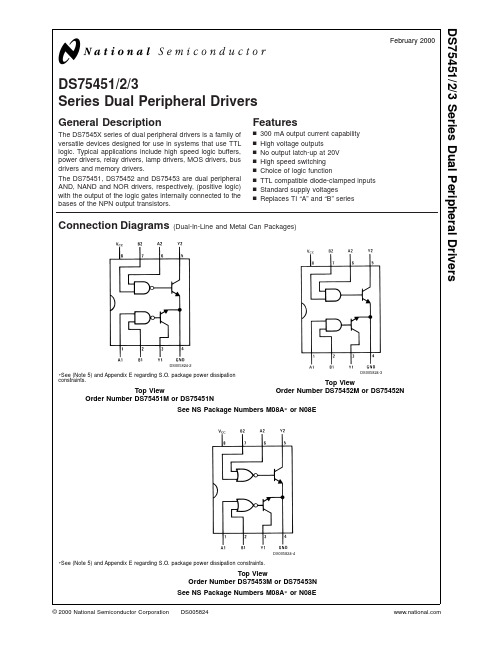
DS75451/2/3Series Dual Peripheral DriversGeneral DescriptionThe DS7545X series of dual peripheral drivers is a family of versatile devices designed for use in systems that use TTL logic.Typical applications include high speed logic buffers,power drivers,relay drivers,lamp drivers,MOS drivers,bus drivers and memory drivers.The DS75451,DS75452and DS75453are dual peripheral AND,NAND and NOR drivers,respectively,(positive logic)with the output of the logic gates internally connected to the bases of the NPN output transistors.Featuresn 300mA output current capability n High voltage outputsn No output latch-up at 20V n High speed switching n Choice of logic functionn TTL compatible diode-clamped inputs n Standard supply voltagesnReplaces TI “A”and “B”seriesConnection Diagrams(Dual-In-Line and Metal Can Packages)DS005824-2*See (Note 5)and Appendix E regarding S.O.package power dissipationconstraints.Top ViewOrder Number DS75451M or DS75451NDS005824-3Top ViewOrder Number DS75452M or DS75452NSee NS Package Numbers M08A *or N08EDS005824-4*See (Note 5)and Appendix E regarding S.O.package power dissipation constraints.Top ViewOrder Number DS75453M or DS75453N See NS Package Numbers M08A *or N08EFebruary 2000DS75451/2/3Series Dual Peripheral Drivers©2000National Semiconductor CorporationDS005824Absolute Maximum Ratings (Note 1)If Military/Aerospace specified devices are required,please contact the National Semiconductor Sales Office/Distributors for availability and specifications.Supply Voltage,(V CC )(Note 2)7.0V Input Voltage5.5V Inter-Emitter Voltage (Note 3) 5.5V Output Voltage (Note 4)30V Output Current (Note 5)300mAMaximum Power (Note 5)Dissipation †at 25˚CMolded DIP Package 957mW SO Package632mWStorage Temperature Range−65˚C to +150˚CLead Temperature (Soldering,4sec.)260˚COperating ConditionsMin Max Units Supply Voltage,(V CC ) 4.75 5.25V Temperature,(T A )0+70˚C†Derate molded package 7.7mW/˚C above 25˚C,derate SO package 7.56mW/˚C above 25˚C.Electrical Characteristics(Notes 6,7)Symbol ParameterConditionsMin Typ Max UnitsV IH High-Level Input Voltage (Figure 7)2V V IL Low-Level Input Voltage 0.8V V I Input Clamp Voltage V CC =Min,I I =−12mA −1.5V V OLLow-Level Output VoltageV CC =Min,(Figure 7)V IL =0.8V I OL =100mA DS75451,DS754530.250.4V I OL =300mA DS75451,DS754530.50.7V V IH=2VI OL =100mA DS754520.250.4V I OL =300mA DS754520.50.7V I OHHigh-Level Output CurrentV CC =Min,(Figure 7)V OH =30V V IH =2VDS75451,DS75453100µA V IL =0.8VDS75452100µA I I Input Current at Maximum Input VoltageV CC =Max,V I =5.5V,(Figure 9)1mA I IH High-Level Input Current V CC =Max,V I =2.4V,(Figure 9)40µA I IL Low-Level Input Current V CC =Max,V I =0.4V,(Figure 8)−1−1.6mA I CCHSupply Current,Outputs HighV CC =Max,(Figure10)V I =5V DS75451711mA V I =0VDS754521114mA V I =5V DS75453811mA I CCLSupply Current,OutputsLowV CC =Max,(Figure10)V I =0V DS754515265mA V I =5VDS754525671mA V I =0V DS754535468mASwitching Characteristics(V CC =5V,T A =25˚C)Symbol ParameterConditionsMinTyp Max Units t PLHPropagation Delay Time,Low-to-High Level OutputC L =15pF,R L =50Ω,I O ≈200mA,(Figure 14)DS754511825ns DS754522635ns DS754531825ns t PHLPropagation Delay Time,High-to-Low Level OutputC L =15pF,R L =50Ω,I O ≈200mA,(Figure 14)DS754511825ns DS754522435ns DS754531625ns t TLH Transition Time,Low-to-High Level OutputC L =15pF,R L =50Ω,I O ≈200mA,(Figure 14)58ns t THLTransition Time,High-to-Low Level OutputC L =15pF,R L =50Ω,I O ≈200mA,(Figure 14)712nsD S 75451/2/3 2Switching Characteristics(Continued)Symbol Parameter Conditions Min Typ Max UnitsV OH High-Level Output Voltage afterSwitching V S=20V,I O≈300mA,(Figure15)V S−6.5mVNote1:“Absolute Maximum Ratings”are those values beyond which the safety of the device cannot be guaranteed.Except for“Operating Temperature Range”theyare not meant to imply that the devices should be operated at these limits.The table of“Electrical Characteristics”provides conditions for actual device operation.Note2:Voltage values are with respect to network ground terminal unless otherwise specified.Note3:The voltage between two emitters of a multiple-emitter transistor.Note4:The maximum voltage which should be applied to any output when it is in the“OFF”state.Note5:Both halves of these dual circuits may conduct rated current simultaneously;however,power dissipation averaged over a short time interval must fall withinthe continuous dissipation rating.Note6:Unless otherwise specified min/max limits apply across0˚C to+70˚C range.All typicals are given for V CC=+5V and T A=25˚C.Note7:All currents into device pins shown as positive,out of device pins as negative,all voltages referenced to ground unless otherwise noted.All values shownas max or min on absolute value basis.Truth Tables(H=high level,L=low level)DS75451A B YL L L(ON State)L H L(ON State)H L L(ON State)H H H(OFF State)DS75452A B YL L H(OFF State)L H H(OFF State)H L H(OFF State)H H L(ON State)DS75453A B YL L L(ON State)L H H(OFF State)H L H(OFF State)H H H(OFF State)DS75451/2/33Schematic DiagramsDS75451DS005824-11Resistor values shown are nominal.DS75452DS005824-12Resistor values shown are nominal.DS75453DS005824-13Resistor values shown are nominal.D S 75451/2/3 4DC Test CircuitsDS005824-15Both inputs is tested simultaneously.FIGURE1.V IH,V OLDS005824-16 Each input is tested separately.FIGURE2.V IL,V OHDS005824-17 Each input is tested separately.FIGURE3.V I,I ILDS005824-18Each input is tested separately.FIGURE4.I I,I IHDS005824-19Each input is tested separately.FIGURE5.I OSDS005824-20Both gates are tested simultaneously.FIGURE6.I CCH,I CCLDS75451/2/35DC Test Circuits(Continued)DS005824-21Circuit Input Under Test Other Input Output Apply Measure DS75451V IH V IH V OH I OL V IL V CC I OL V OL DS75452V IH V IH I OL V OL V IL V CC V OH I OH DS75453V IH Gnd V OH I OH V ILV ILI OLV OHFIGURE 7.V IH ,V IL ,I OH ,V OLDS005824-22Note A:Each input is tested separately.Note B :When testing DS75453input not under test is grounded.For all other circuits it is at 4.5V.FIGURE 8.V I ,V ILDS005824-23Each input is tested separately.FIGURE 9.I I ,I IHDS005824-24Both gates are tested simultaneously.FIGURE 10.I CCH ,I CCL for AND,NAND CircuitsDS005824-25Both gates are tested simultaneously.FIGURE 11.I CCH ,I CCL for OR,NOR CircuitsD S 75451/2/3 6AC Test Circuits and Switching Time WaveformsDS005824-26DS005824-27Note 1:The pulse generator has the following characteristics:PRR =1MHz,Z OUT ≈50Ω.Note 2:C L includes probe and jig capacitance.FIGURE 12.Propagation Delay Times,Each GateDS005824-28DS005824-29Note 1:The pulse generator has the following characteristics:duty cycle ≤1%,Z OUT ≈50Ω.Note 2:C L includes probe and jig capacitance.FIGURE 13.Switching Times,Each TransistorDS75451/2/37AC Test Circuits and Switching Time Waveforms(Continued)DS005824-30DS005824-31Note 1:The The pulse generator has the following characteristics:PRR =1.0MHz,Z OUT ≈50Ω.Note 2:C L includes probe and jig capacitance.FIGURE 14.Switching Times of Complete DriversD S 75451/2/3 8AC Test Circuits and Switching Time Waveforms(Continued)Typical Performance CharacteristicsDS005824-32DS005824-33Note 1:The pulse generator has the following characteristics:PRR =12.5kHz,Z OUT ≈50Ω.Note 2:C L includes probe and jig capacitance.FIGURE tch-UP Test of Complete DriversDS005824-37FIGURE 16.Transistor Collector-Emitter Saturation Voltage vs Collector CurrentDS75451/2/39Typical ApplicationsDS005824-46*Optional keep-alive resistors maintain off-state lamp current at ≈10%to reduce surge current.FIGURE 17.Dual Lamp or Relay DriverDS005824-47FIGURE plementary DriverDS005824-48FIGURE 19.TTL or DTL Positive Logic-Level DetectorD S 75451/2/310DS75451/2/3 Typical Applications(Continued)DS005824-49*The two input resistors must be adjusted for the level of MOS input.FIGURE20.MOS Negative Logic-Level Detector11Typical Applications(Continued)DS005824-50FIGURE 21.Logic Signal ComparatorDS005824-51*If inputs are unused,they should be connected to +5V through a 1k resistor.DS005824-52Low output occurs only when inputs are low simultaneously.FIGURE 22.In-Phase DetectorD S 75451/2/3 12Physical Dimensionsinches (millimeters)unless otherwise notedSO Package (M)Order Number DS75451M,DS75452M,DS75453MNS Package Number M08AMolded Dual-In-Line Package (N)Order Number DS75451N,DS75452N,DS75453NNS Package Number N08EDS75451/2/313NotesLIFE SUPPORT POLICYNATIONAL’S PRODUCTS ARE NOT AUTHORIZED FOR USE AS CRITICAL COMPONENTS IN LIFE SUPPORT DEVICES OR SYSTEMS WITHOUT THE EXPRESS WRITTEN APPROVAL OF THE PRESIDENT AND GENERAL COUNSEL OF NATIONAL SEMICONDUCTOR CORPORATION.As used herein:1.Life support devices or systems are devices or systems which,(a)are intended for surgical implant into the body,or (b)support or sustain life,and whose failure to perform when properly used in accordance with instructions for use provided in the labeling,can be reasonably expected to result in a significant injury to the user.2.A critical component is any component of a life support device or system whose failure to perform can be reasonably expected to cause the failure of the life support device or system,or to affect its safety or effectiveness.National Semiconductor Corporation AmericasTel:1-800-272-9959Fax:1-800-737-7018Email:support@National Semiconductor EuropeFax:+49(0)180-5308586Email:europe.support@Deutsch Tel:+49(0)6995086208English Tel:+44(0)8702402171Français Tel:+33(0)141918790National Semiconductor Asia Pacific Customer Response Group Tel:65-2544466Fax:65-2504466Email:ap.support@National Semiconductor Japan Ltd.Tel:81-3-5639-7560Fax:81-3-5639-7507D S 75451/2/3S e r i e s D u a l P e r i p h e r a l D r i v e r sNational does not assume any responsibility for use of any circuitry described,no circuit patent licenses are implied and National reserves the right at any time without notice to change said circuitry and specifications.。
AD7543中文资料引脚图应用电路图引言数/模转换(D/A)电路,是数字系统中常用的电路之一,其主要作用是把数字信号转换成模拟信号,通常是利用专用的数/模转换(D/A)芯片来实现的。
AD7543是Analog D evice公司生产的的12位数/模转换(D/A)芯片,它采用串行数据输入形式,即数字信号被一位一位地写入AD7543数/模转换(D/A)芯片中,因此,AD7543要与一个控制器配合使用才能发挥作用。
常规的方法,是以CPU作为控制部件,通过软件编程的方式来控制AD7543,从而实现数/模转换功能的。
软件实现法虽然简单,但必将会占用大量的CP U时间,削弱了CPU实时处理能力,降低了系统的可靠性。
针对以上情况,在此设计了基于可编程逻辑器件(FPGA)数/模转换电路,利用可编程逻辑器件(FP-GA)直接控制模转换(D/A)芯片AD7543进行数/模(D/A)转换,取代传统的“CPU+专用的数/模转换(D/A)芯片”设计结构,有利于提高系统的抗干扰能力和可靠性。
1 AD7543简介1.1 AD7543主要特性AD7543主要特性为:分辨率:12位;非线性误差:±1/2 LSB;输入方式:串行正或负选通;初始化:异步输入清零方式;工作电压:+5 V;最大功耗:40 mW。
1.2 封装形式和引脚功能AD7543有三种封装形式:16引脚的DIP和20引脚的PCCC与PLCC,其封装形式如图1所示,设计者可根据实现需求进行选择,其引脚功能说明如下:OUT1:数/模转换(D/A)器电流输出端,通常接到放大器正输入端;OUT2:数/模转换(D/A)器电流输出端,通常接到模拟地;AGND:模拟地端,接到模拟地;STB1:寄存器A选通1信号输入端;LD1:寄存器B装人选通1输入端,LD1和LD2都为低电平时,寄存器A的内容被装入到寄存器B中;N/C:悬空;SRI:串行数据输入端,与寄存器A低位相连;STB2:寄存器A选通2信号输入端;LD2:寄存器B装入选通2输入端,LD1和LD2都为低电平时,寄存器A的内容被装入到寄存器B中;STB3:寄存器A选通3信号输入端;STB4:寄存器A选通4信号输入端;DGND:数字地端;CLR:异步清寄存器B输入端,当为低电平时,清寄存器B内容,寄存器A内容不变;VDD:5 V供电输入端;VREF:参考电压输入端;RBF:反馈输入端。
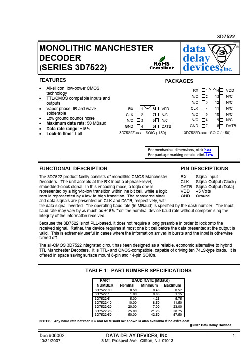
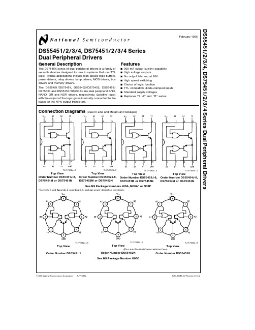
TL F 5824DS55451 2 3 4 DS75451 2 3 4Series Dual Peripheral DriversFebruary 1995DS55451 2 3 4 DS75451 2 3 4Series Dual Peripheral DriversGeneral DescriptionThe DS7545X series of dual peripheral drivers is a family of versatile devices designed for use in systems that use TTL logic Typical applications include high speed logic buffers power drivers relay drivers lamp drivers MOS drivers bus drivers and memory driversThe DS55451 DS75451 DS55452 DS75452 DS55453 DS75453and DS55454 DS75454are dual peripheral AND NAND OR and NOR drivers respectively (positive logic)with the output of the logic gates internally connected to the bases of the NPN output transistorsFeaturesY 300mA output current capability Y High voltage outputsY No output latch-up at 20V Y High speed switching Y Choice of logic functionY TTL compatible diode-clamped inputs Y Standard supply voltagesYReplaces TI ‘‘A’’and ‘‘B’’seriesConnection Diagrams (Dual-In-Line and Metal Can Packages)TL F 5824–2Top ViewOrder Number DS55451J-8 DS75451M or DS75451N TL F 5824–3Top ViewOrder Number DS55452J-8 DS75452M or DS75452N TL F 5824–4Top ViewOrder Number DS55453J-8 DS75453M or DS75453N TL F 5824–5Top ViewOrder Number DS55454J-8 DS75454M or DS75454NSee NS Package Numbers J08A M08A or N08ESee Note 5and Appendix E regarding S O package power dissipation constraintsTL F 5824–6Top ViewOrder Number DS55451HTL F 5824–7Top View(Pin 4is in Electrical Contact with the Case)Order Number DS55452H TL F 5824–8Top ViewOrder Number DS55453HSee NS Package Number H08CC 1995National Semiconductor Corporation RRD-B30M105 Printed in U S AAbsolute Maximum Ratings(Note1)If Military Aerospace specified devices are required please contact the National Semiconductor Sales Office Distributors for availability and specifications Supply Voltage (V CC)(Note2)7 0V Input Voltage5 5V Inter-Emitter Voltage(Note3)5 5V Output Voltage(Note4)DS55451 DS75451 DS55452 DS75452 30V DS55453 DS75453 DS55454 DS75454Output Current(Note5)DS55451 DS75451 DS55452 DS75452 300mA DS55453 DS75453 DS55454 DS75454DS75451 2 3 4Maximum Power(Note5)Dissipation at25 CCavity Package1090mW Molded DIP Package957mW TO-5Package760mW SO Package632mW Storage Temperature Range b65 C to a150 C Lead Temperature(Soldering 4sec )260 C Operating ConditionsMin Max Units Supply Voltage (V CC)DS5545X4 55 5V DS7545X4 755 25V Temperature (T A)DS5545X b55a125 C DS7545X0a70 C Derate cavity package7 3mW C above25 C derate molded package 7 7mW C above25 C derate TO-5package5 1mW C above25 C derate SO package7 56mW C above25 CElectrical CharacteristicsDS55451 DS75451 DS55452 DS75452 DS55453 DS75453 DS55454 DS75454(Notes6and7)Symbol Parameter Conditions Min Typ Max Units V IH High-Level Input Voltage(Figure7)2V V IL Low-Level Input Voltage0 8V V I Input Clamp Voltage V CC e Min I I e b12mA b1 5V V OL Low-Level Output Voltage V CC e Min V IL e0 8V I OL e100mA DS55451 DS554530 250 5V(Figure7)DS75451 DS754530 250 4VI OL e300mA DS55451 DS554530 50 8VDS75451 DS754530 50 7VV IH e2V I OL e100mA DS55452 DS554540 250 5VDS75452 DS754540 250 4VI OL e300mA DS55452 DS554540 50 8VDS75452 DS754540 50 7V I OH High-Level Output Current V CC e Min V OH e30V V IH e2V DS55451 DS55453300m A(Figure7)DS75451 DS75453100m AV IL e0 8V DS55452 DS55454300m ADS75452 DS75454100m A I I Input Current at Maximum V CC e Max V I e5 5V (Figure9)1mAInput VoltageI IH High-Level Input Current V CC e Max V I e2 4V (Figure9)40m A I IL Low-Level Input Current V CC e Max V I e0 4V (Figure8)b1b1 6mA I CCH Supply Current Outputs High V CC e Max V I e5V DS55451 DS75451711mA(Figure10)VI e0V DS55452 DS754521114mAV I e5V DS55453 DS75453811mAV I e0V DS55454 DS754541317mA I CCL Supply Current Outputs Low V CC e Max V I e0V DS55451 DS754515265mA(Figure10)VI e5V DS55452 DS754525671mAV I e0V DS55453 DS754535468mAV I e5V DS55454 DS754546179mA2Switching CharacteristicsDS55451 DS75451 DS55452 DS75452 DS55453 DS75453 DS55454 DS75454(V CC e5V T A e25 C)Symbol Parameter Conditions Min Typ Max Units t PLH Propagation Delay Time Low-to-High C L e15pF R L e50X DS55451 DS754511825ns Level Output I O 200mA (Figure14)DS55452 DS754522635nsDS55453 DS754531825nsDS55454 DS754542735ns t PHL Propagation Delay Time High-to-Low C L e15pF R L e50X DS55451 DS754511825ns Level Output I O 200mA (Figure14)DS55452 DS754522435nsDS55453 DS754531625nsDS55454 DS754542435ns t TLH Transition Time Low-to-High Level C L e15pF R L e50X I O 200mA58ns Output(Figure14)t THL Transition Time High-to-Low Level C L e15pF R L e50X I O 200mA712ns Output(Figure14)V OH High-Level Output Voltage after V S e20V I O 300mA (Figure15)V S b6 5mV SwitchingNote1 ‘‘Absolute Maximum Ratings’’are those values beyond which the safety of the device cannot be guaranteed Except for‘‘Operating Temperature Range’’they are not meant to imply that the devices should be operated at these limits The table of‘‘Electrical Characteristics’’provides conditions for actual device operationNote2 Voltage values are with respect to network ground terminal unless otherwise specifiedNote3 The voltage between two emitters of a multiple-emitter transistorNote4 The maximum voltage which should be applied to any output when it is in the‘‘OFF’’stateNote5 Both halves of these dual circuits may conduct rated current simultaneously however power dissipation averaged over a short time interval must fall within the continuous dissipation ratingNote6 Unless otherwise specified min max limits apply across the b55 C to a125 C temperature range for the DS55450series and across the0 C to a70 C range for the DS7545X series All typicals are given for V CC e a5V and T A e25 CNote7 All currents into device pins shown as positive out of device pins as negative all voltages referenced to ground unless otherwise noted All values shown as max or min on absolute value basis3Truth Tables(H e high level L e low level)DS55451 DS75451A B YL L L(ON State) L H L(ON State) H L L(ON State) H H H(OFF State)DS55452 DS75452A B YL L H(OFF State) L H H(OFF State) H L H(OFF State) H H L(ON State)DS55453 DS75453A B YL L L(ON State) L H H(OFF State) H L H(OFF State) H H H(OFF State)DS55454 DS75454A B YL L H(OFF State) L H L(ON State) H L L(ON State) H H L(ON State)Schematic DiagramsDS55451 DS75451TL F 5824–11 Resistor values shown are nominalDS55452 DS75452TL F 5824–12 Resistor values shown are nominalDS55453 DS75453TL F 5824–13 Resistor values shown are nominalDS55454 DS75454TL F 5824–14 Resistor values shown are nominal4DC Test CircuitsTL F 5824–15Both inputs are tested simultaneouslyFIGURE1 V IH V OLTL F 5824–16Each input is tested separatelyFIGURE2 V IL V OHTL F 5824–17Each input is tested separatelyFIGURE3 V I I ILTL F 5824–18Each input is tested separatelyFIGURE4 I I I IHTL F 5824–19Each input is tested separatelyFIGURE5 I OSTL F 5824–20Both gates are tested simultaneouslyFIGURE6 I CCH I CCLTL F 5824–21Circuit UnderInputTestOtherInputOutputApply MeasureDS55451V IH V IH V OH I OHV IL V CC I OL V OLDS55452V IH V IH I OL V OLV IL V CC V OH I OHDS55453V IH Gnd V OH I OHV IL V IL I OL V OHDS55454V IH Gnd I OL V OLV IL V IL V OH I OHFIGURE7 V IH V IL I OH V OLNote A Each input is tested separatelyNote B When testing DS55453 DS75453DS55454 DS75454 input notunder test is groundedFor all other circuits it is at4 5VTL F 5824–22FIGURE8 V I V ILEach input is tested separately TL F 5824–23FIGURE9 I I I IHBoth gates are tested simultaneously TL F 5824–24FIGURE10 I CCH I CCL for AND NAND CircuitsBoth gates are tested simultaneously TL F 5824–25FIGURE11 I CCH I CCL for OR NOR Circuits5AC Test Circuits and Switching Time WaveformsTL F 5824–26TL F 5824–27 Note1 The pulse generator has the following characteristics PRR e1MHz Z OUT 50XNote2 C L includes probe and jig capacitanceFIGURE12 Propagation Delay Times Each GateTL F 5824–28TL F 5824–29 Note1 The pulse generator has the following characteristics duty cycle s1% Z OUT 50XNote2 C L includes probe and jig capacitanceFIGURE13 Switching Times Each Transistor6AC Test Circuits and Switching Time Waveforms(Continued)TL F 5824–30Note1 The pulse generator has the following characteristics PRR e1 0MHz Z OUT 50X TL F 5824–31 Note2 C L includes probe and jig capacitanceFIGURE14 Switching Times of Complete Drivers7AC Test Circuits and Switching Time Waveforms(Continued)TL F 5824–32TL F 5824–33 Note1 The pulse generator has the following characteristics PRR e12 5kHz Z OUT 50XNote2 C L includes probe and jig capacitanceFIGURE15 Latch-UP Test of Complete DriversTypical Performance CharacteristicsTL F 5824–37FIGURE16 Transistor Collector-Emitter Saturation Voltage vs Collector Current8Typical ApplicationsTL F 5824–46 Optional keep-alive resistors maintain off-state lamp current at 10%to reduce surge currentFIGURE17 Dual Lamp or Relay DriverTL F 5824–47FIGURE18 Complementary Driver9Typical Applications(Continued)TL F 5824–48FIGURE19 TTL or DTL Positive Logic-Level DetectorTL F 5824–49 The two input resistors must be adjusted for the level of MOS inputFIGURE20 MOS Negative Logic-Level DetectorTL F 5824–50FIGURE21 Logic Signal Comparator10Typical Applications(Continued)TL F 5824–51If inputs are unused they should be connected to a5V through a1k resistorTL F 5824–52Low output occurs only when inputs are low simultaneouslyFIGURE22 In-Phase DetectorTL F 5824–53FIGURE23 Multifunction Logic-Signal Comparator11Typical Applications(Continued)TL F 5824–54FIGURE24 Alarm Detector1213Physical Dimensions inches(millimeters)Metal Can Package(H)Order Number DS55451H DS55452H or DS55453HNS Package Number H08CCeramic Dual-In-Line Package(J)Order Number DS55451J-8 DS55452J-8DS55453J-8or DS55454J-8NS Package Number J08A14Physical Dimensions inches(millimeters)(Continued)SO Package(M)Order Number DS75451M DS75452M DS75453M or DS75454MNS Package Number M08AMolded Dual-In-Line Package(N)Order Number DS75451N DS75452N DS75453N DS75454NNS Package Number N08E15D S 55451 2 3 4 D S 75451 2 3 4S e r i e s D u a l P e r i p h e r a l D r i v e r sLIFE SUPPORT POLICYNATIONAL’S PRODUCTS ARE NOT AUTHORIZED FOR USE AS CRITICAL COMPONENTS IN LIFE SUPPORT DEVICES OR SYSTEMS WITHOUT THE EXPRESS WRITTEN APPROVAL OF THE PRESIDENT OF NATIONAL SEMICONDUCTOR CORPORATION As used herein1 Life support devices or systems are devices or2 A critical component is any component of a life systems which (a)are intended for surgical implantsupport device or system whose failure to perform can into the body or (b)support or sustain life and whosebe reasonably expected to cause the failure of the life failure to perform when properly used in accordancesupport device or system or to affect its safety or with instructions for use provided in the labeling caneffectiveness be reasonably expected to result in a significant injuryto the userNational SemiconductorNational Semiconductor National Semiconductor National Semiconductor CorporationEurope Hong Kong Ltd Japan Ltd 1111West Bardin Road Fax (a 49)0-180-530858613th Floor Straight Block Tel 81-043-299-2309。
集成电路英文代码及中文对照(一)我的文摘2009-11-21 11:32:53 阅读111 评论0 字号:大中小订阅性能说明产品名称型号规格LMLM24J 四运放(军用级)LM148J 通用四运放LM1875T 无线电控制/接收器LM224J 四运放(工业级)LM258N 分离式双电源双运放LM2901N 四电压比较器LM2904N 四运放LM301AN 通用运算放大器LM308N 单比较器LM311P 单比较器LM317L 可调三端稳压器/100mALM317T 可调三端稳压器/1.5ALM317K 可调三端稳压器/3ALM318 高速宽带运放LM324K 通用四运放LM331N V-F/F-V转换器LM336-2.5V 基准电压电路LM336 5V 基准电压电路LM337T 基准电压电路1ALM338K 可调三端稳压器5ALM339N 四比较器LM348N 四741运放LM358N 低功耗双运放LM361N 高速差动比较器LM386N 声频功率放大器LM3914N 十段点线显示驱动LM393N 低功耗低失调双比较器LM399H 精密基准源(6.9)LM723CN 可调正式负稳压器LM733CN 视频放大器LM741J 单运放LM741CN 双运放NENE521 高速双差分比较器NE5532 双运放NE5534 双运放NE555N 单运放NE555J 时基电路军品极NE556 双级型双时基电路NE564 锁相环NE565 锁相环NE567 音调译码器NE592 视频放大器OPOP07 低噪声运放OP27 超低噪声精密运放OP37 超低噪声精密运放光电耦合4N25 晶体管输出4N25MC 晶体管输出4N26 晶体管输出4N27 晶体管输出4N28 晶体管输出4N29 达林顿输出4N30 达林顿输出4N31 达林顿输出4N32 达林顿输出4N33 达林顿输出4N33MC 达林顿输出4N35 达林顿输出4N36 晶体管输出4N37 晶体管输出4N38 晶体管输出4N39 可控硅输出6N135 高速光耦晶体管输出6N136 高速光耦晶体管输出6N137 高速光耦晶体管输出6N138 达林顿输出6N139 达林顿输出MOC3020 可控硅驱动输出MOC3021 可控硅驱动输出MOC3023 可控硅驱动输出MOC3030 可控硅驱动输出MOC3040 过零触发可控硅输出MOC3041 过零触发可控硅输出MOC3061 过零触发可控硅输出MOC3081 过零触发可控硅输出TLP521-1 单光耦TLP521-2 双光耦TLP521-4 四光耦TLP621 四光耦TIL113 达林顿输出TIL117 TLL逻辑输出PC814 单光耦PC817 单光耦H11A2 晶体管输出H11D1 高压晶体管输出H11G2 电阻达林顿输出LFLF347N 宽带JFET输入四运放LF351N 宽带JFET输入运放LF353N JFET输入宽带运放LF355N JFET输入运放LF357N JFET宽带非全裣运放LF398N 采样/保持电路LF412N 低偏差飘移输入运放MCMC1377 彩色电视编码器MC1403 精密电压基准源(2.5)MC1413 周边七段驱动阵列MC1416 周边七段驱动陈列MC14409 二进制脉冲拨号器MC14433 3位半A/D转换器MC14489 多字符LED显示驱动器MC145026 编码器VD5026 编码器MC145027 译码器VD5027 译码器MC145028 译码器MC145030 编码译码器MC145106 频率合成器MC145146 4位数据总线TLTL062 低功耗JEFT输入双运放TL072 低噪声JEFTTL082TL084TL431TL494ULNULN2003 周边七段驱动陈列ULN2004 周边七段驱动陈列ULN2803 周边八段驱动陈列ULN2804 周边八段驱动陈列ICLICL7106 3位ADC/驱动LCDICL7107 3位半ADC/驱动LEDICL7109 4位半ADC/驱动LEDICL7129 4位半ADC/LCD驱动ICL7135 ADC/LCD驱动BCD输出ICL7136 3位半CMOSADC/LCD驱动ICL7218 CMOS低功耗运算放大器ICL7650 整零运放斩波ICL7652 整零运放斩波ICL7660 CMOS直流-直流转换器ICL8038 函数信号发生器ICL8049 反对数放大器CACA3140 单BIMOS运行CA3240 单BIMOS运行UCUC3842 WM电流型控制器UC3845 PWM电流型控制器DSDS12887 非易失实时时钟芯片L3845 中继接口电路SGSG3524 PWM解调调制器SG3525 PWM解调调制器20106 前置放大器MTMT8814 8x12模拟交换矩阵MT8816 8x模拟交换矩阵MT8870 综合DTMF接收器MT8870 综合DTMF接收器MT8880 综合DTMF发生接收器MIC24LC01 128x8串行EEPROM24LC02 256x8串行EEPROM24LC04 512x8串行EEPROM24LC16 2Kx8串行EEPROM93LC46 64x16串行EEPROM93LC56 256x16串行EEPROM93LC66 512x8 256x16 EEPROMPIC16C52 384x12 单片机PIC16C54 512x12 单片机PCI16C56 512x12 单片机PIC16C57 2048x12 单片机ATAT24C01 128x8串行EEPROMAT24C02 256x8串行EEPROMAT24C04 512x8串行EEPROMAT24C16 2Kx8串行EEPROMAT93C46 64x16串行EEPROMAT93C56 256x16串行EEPROMATF16V8 FLASH200门ATF20V8 FLASH300门高速ATF22V10 FLASH500门高速低电流AT28C16 2Kx8CMOS并行EEPROMAT28C17 2Kx8CMOS并行EEPROMAT28C64 8Kx8并行EEPROMAT28C256 32Kx8并行EEPROMAT28F010 128Kx8并行EEPROMA29C040 512Kx8 FLASH EEPROMHM6116 2Kx8 CMOS 静态PAMHY6264 8Kx8 CMOS 静态RAMHM6264 8Kx8 CMOS 静态RAMIS62C64 8Kx8 高速CMOS 静态RAMHY62256 32Kx8 CMOS 静态RAMHM62256 32Kx8 CMOS 静态RAMHM628128 128Kx8 CMOS 静态RAMHM628256 256Kx8 CMOS 静态RAMHM628512 512Kx8 CMOS 静态RAMHM628512 512Kx8 CMOS 静态RAM TCMTCM5087 双音调发生器MM5832 实时钟电路TCTC14433 3位半A/D转换器TC232 并行/串行接口电路TC7106 3位半ADC/LCD驱动TC7107 3位半ADC/LED驱动TC7116 3位半ADC/LCD驱动带保TC7129 4位半ADC/LCDTC7135 4位半ADC/LCD,BCD输出TC7650 整零运放斩波7575107 四差分线驱动器75174 四差分线驱动器75175 三态四差分接收器75176 差分总线接收器75188 四线驱动器75189 四线驱动器75451 双外围驱动器75452 双外围驱动器集成电路英文代码及中文对照(二)我的文摘2009-11-21 11:37:11 阅读191 评论0 字号:大中小订阅。
DS75451/2/3Series Dual Peripheral DriversGeneral DescriptionThe DS7545X series of dual peripheral drivers is a family of versatile devices designed for use in systems that use TTL logic.Typical applications include high speed logic buffers,power drivers,relay drivers,lamp drivers,MOS drivers,bus drivers and memory drivers.The DS75451,DS75452and DS75453are dual peripheral AND,NAND and NOR drivers,respectively,(positive logic)with the output of the logic gates internally connected to the bases of the NPN output transistors.Featuresn 300mA output current capability n High voltage outputsn No output latch-up at 20V n High speed switching n Choice of logic functionn TTL compatible diode-clamped inputs n Standard supply voltagesnReplaces TI “A”and “B”seriesConnection Diagrams(Dual-In-Line and Metal Can Packages)DS005824-2*See (Note 5)and Appendix E regarding S.O.package power dissipationconstraints.Top ViewOrder Number DS75451M or DS75451NDS005824-3Top ViewOrder Number DS75452M or DS75452NSee NS Package Numbers M08A *or N08EDS005824-4*See (Note 5)and Appendix E regarding S.O.package power dissipation constraints.Top ViewOrder Number DS75453M or DS75453N See NS Package Numbers M08A *or N08EFebruary 2000DS75451/2/3Series Dual Peripheral Drivers©2000National Semiconductor CorporationDS005824Absolute Maximum Ratings (Note 1)If Military/Aerospace specified devices are required,please contact the National Semiconductor Sales Office/Distributors for availability and specifications.Supply Voltage,(V CC )(Note 2)7.0V Input Voltage5.5V Inter-Emitter Voltage (Note 3) 5.5V Output Voltage (Note 4)30V Output Current (Note 5)300mAMaximum Power (Note 5)Dissipation †at 25˚CMolded DIP Package 957mW SO Package632mWStorage Temperature Range−65˚C to +150˚CLead Temperature (Soldering,4sec.)260˚COperating ConditionsMin Max Units Supply Voltage,(V CC ) 4.75 5.25V Temperature,(T A )0+70˚C†Derate molded package 7.7mW/˚C above 25˚C,derate SO package 7.56mW/˚C above 25˚C.Electrical Characteristics(Notes 6,7)Symbol ParameterConditionsMin Typ Max UnitsV IH High-Level Input Voltage (Figure 7)2V V IL Low-Level Input Voltage 0.8V V I Input Clamp Voltage V CC =Min,I I =−12mA −1.5V V OLLow-Level Output VoltageV CC =Min,(Figure 7)V IL =0.8V I OL =100mA DS75451,DS754530.250.4V I OL =300mA DS75451,DS754530.50.7V V IH=2VI OL =100mA DS754520.250.4V I OL =300mA DS754520.50.7V I OHHigh-Level Output CurrentV CC =Min,(Figure 7)V OH =30V V IH =2VDS75451,DS75453100µA V IL =0.8VDS75452100µA I I Input Current at Maximum Input VoltageV CC =Max,V I =5.5V,(Figure 9)1mA I IH High-Level Input Current V CC =Max,V I =2.4V,(Figure 9)40µA I IL Low-Level Input Current V CC =Max,V I =0.4V,(Figure 8)−1−1.6mA I CCHSupply Current,Outputs HighV CC =Max,(Figure10)V I =5V DS75451711mA V I =0VDS754521114mA V I =5V DS75453811mA I CCLSupply Current,OutputsLowV CC =Max,(Figure10)V I =0V DS754515265mA V I =5VDS754525671mA V I =0V DS754535468mASwitching Characteristics(V CC =5V,T A =25˚C)Symbol ParameterConditionsMinTyp Max Units t PLHPropagation Delay Time,Low-to-High Level OutputC L =15pF,R L =50Ω,I O ≈200mA,(Figure 14)DS754511825ns DS754522635ns DS754531825ns t PHLPropagation Delay Time,High-to-Low Level OutputC L =15pF,R L =50Ω,I O ≈200mA,(Figure 14)DS754511825ns DS754522435ns DS754531625ns t TLH Transition Time,Low-to-High Level OutputC L =15pF,R L =50Ω,I O ≈200mA,(Figure 14)58ns t THLTransition Time,High-to-Low Level OutputC L =15pF,R L =50Ω,I O ≈200mA,(Figure 14)712nsD S 75451/2/3 2Switching Characteristics(Continued)Symbol Parameter Conditions Min Typ Max UnitsV OH High-Level Output Voltage afterSwitching V S=20V,I O≈300mA,(Figure15)V S−6.5mVNote1:“Absolute Maximum Ratings”are those values beyond which the safety of the device cannot be guaranteed.Except for“Operating Temperature Range”theyare not meant to imply that the devices should be operated at these limits.The table of“Electrical Characteristics”provides conditions for actual device operation.Note2:Voltage values are with respect to network ground terminal unless otherwise specified.Note3:The voltage between two emitters of a multiple-emitter transistor.Note4:The maximum voltage which should be applied to any output when it is in the“OFF”state.Note5:Both halves of these dual circuits may conduct rated current simultaneously;however,power dissipation averaged over a short time interval must fall withinthe continuous dissipation rating.Note6:Unless otherwise specified min/max limits apply across0˚C to+70˚C range.All typicals are given for V CC=+5V and T A=25˚C.Note7:All currents into device pins shown as positive,out of device pins as negative,all voltages referenced to ground unless otherwise noted.All values shownas max or min on absolute value basis.Truth Tables(H=high level,L=low level)DS75451A B YL L L(ON State)L H L(ON State)H L L(ON State)H H H(OFF State)DS75452A B YL L H(OFF State)L H H(OFF State)H L H(OFF State)H H L(ON State)DS75453A B YL L L(ON State)L H H(OFF State)H L H(OFF State)H H H(OFF State)DS75451/2/33Schematic DiagramsDS75451DS005824-11Resistor values shown are nominal.DS75452DS005824-12Resistor values shown are nominal.DS75453DS005824-13Resistor values shown are nominal.D S 75451/2/3 4DC Test CircuitsDS005824-15Both inputs is tested simultaneously.FIGURE1.V IH,V OLDS005824-16 Each input is tested separately.FIGURE2.V IL,V OHDS005824-17 Each input is tested separately.FIGURE3.V I,I ILDS005824-18Each input is tested separately.FIGURE4.I I,I IHDS005824-19Each input is tested separately.FIGURE5.I OSDS005824-20Both gates are tested simultaneously.FIGURE6.I CCH,I CCLDS75451/2/35DC Test Circuits(Continued)DS005824-21Circuit Input Under Test Other Input Output Apply Measure DS75451V IH V IH V OH I OL V IL V CC I OL V OL DS75452V IH V IH I OL V OL V IL V CC V OH I OH DS75453V IH Gnd V OH I OH V ILV ILI OLV OHFIGURE 7.V IH ,V IL ,I OH ,V OLDS005824-22Note A:Each input is tested separately.Note B :When testing DS75453input not under test is grounded.For all other circuits it is at 4.5V.FIGURE 8.V I ,V ILDS005824-23Each input is tested separately.FIGURE 9.I I ,I IHDS005824-24Both gates are tested simultaneously.FIGURE 10.I CCH ,I CCL for AND,NAND CircuitsDS005824-25Both gates are tested simultaneously.FIGURE 11.I CCH ,I CCL for OR,NOR CircuitsD S 75451/2/3 6AC Test Circuits and Switching Time WaveformsDS005824-26DS005824-27Note 1:The pulse generator has the following characteristics:PRR =1MHz,Z OUT ≈50Ω.Note 2:C L includes probe and jig capacitance.FIGURE 12.Propagation Delay Times,Each GateDS005824-28DS005824-29Note 1:The pulse generator has the following characteristics:duty cycle ≤1%,Z OUT ≈50Ω.Note 2:C L includes probe and jig capacitance.FIGURE 13.Switching Times,Each TransistorDS75451/2/37AC Test Circuits and Switching Time Waveforms(Continued)DS005824-30DS005824-31Note 1:The The pulse generator has the following characteristics:PRR =1.0MHz,Z OUT ≈50Ω.Note 2:C L includes probe and jig capacitance.FIGURE 14.Switching Times of Complete DriversD S 75451/2/3 8AC Test Circuits and Switching Time Waveforms(Continued)Typical Performance CharacteristicsDS005824-32DS005824-33Note 1:The pulse generator has the following characteristics:PRR =12.5kHz,Z OUT ≈50Ω.Note 2:C L includes probe and jig capacitance.FIGURE tch-UP Test of Complete DriversDS005824-37FIGURE 16.Transistor Collector-Emitter Saturation Voltage vs Collector CurrentDS75451/2/39Typical ApplicationsDS005824-46*Optional keep-alive resistors maintain off-state lamp current at ≈10%to reduce surge current.FIGURE 17.Dual Lamp or Relay DriverDS005824-47FIGURE plementary DriverDS005824-48FIGURE 19.TTL or DTL Positive Logic-Level DetectorD S 75451/2/310DS75451/2/3 Typical Applications(Continued)DS005824-49*The two input resistors must be adjusted for the level of MOS input.FIGURE20.MOS Negative Logic-Level Detector11Typical Applications(Continued)DS005824-50FIGURE 21.Logic Signal ComparatorDS005824-51*If inputs are unused,they should be connected to +5V through a 1k resistor.DS005824-52Low output occurs only when inputs are low simultaneously.FIGURE 22.In-Phase DetectorD S 75451/2/3 12Physical Dimensionsinches (millimeters)unless otherwise notedSO Package (M)Order Number DS75451M,DS75452M,DS75453MNS Package Number M08AMolded Dual-In-Line Package (N)Order Number DS75451N,DS75452N,DS75453NNS Package Number N08EDS75451/2/313NotesLIFE SUPPORT POLICYNATIONAL’S PRODUCTS ARE NOT AUTHORIZED FOR USE AS CRITICAL COMPONENTS IN LIFE SUPPORT DEVICES OR SYSTEMS WITHOUT THE EXPRESS WRITTEN APPROVAL OF THE PRESIDENT AND GENERAL COUNSEL OF NATIONAL SEMICONDUCTOR CORPORATION.As used herein:1.Life support devices or systems are devices or systems which,(a)are intended for surgical implant into the body,or (b)support or sustain life,and whose failure to perform when properly used in accordance with instructions for use provided in the labeling,can be reasonably expected to result in a significant injury to the user.2.A critical component is any component of a life support device or system whose failure to perform can be reasonably expected to cause the failure of the life support device or system,or to affect its safety or effectiveness.National Semiconductor Corporation AmericasTel:1-800-272-9959Fax:1-800-737-7018Email:support@National Semiconductor EuropeFax:+49(0)180-5308586Email:europe.support@Deutsch Tel:+49(0)6995086208English Tel:+44(0)8702402171Français Tel:+33(0)141918790National Semiconductor Asia Pacific Customer Response Group Tel:65-2544466Fax:65-2504466Email:ap.support@National Semiconductor Japan Ltd.Tel:81-3-5639-7560Fax:81-3-5639-7507D S 75451/2/3S e r i e s D u a l P e r i p h e r a l D r i v e r sNational does not assume any responsibility for use of any circuitry described,no circuit patent licenses are implied and National reserves the right at any time without notice to change said circuitry and specifications.。
元器件交易网IMPORTANT NOTICETexas Instruments and its subsidiaries (TI) reserve the right to make changes to their products or to discontinueany product or service without notice, and advise customers to obtain the latest version of relevant informationto verify, before placing orders, that information being relied on is current and complete. All products are soldsubject to the terms and conditions of sale supplied at the time of order acknowledgement, including thosepertaining to warranty, patent infringement, and limitation of liability.TI warrants performance of its semiconductor products to the specifications applicable at the time of sale inaccordance with TI’s standard warranty. Testing and other quality control techniques are utilized to the extentTI deems necessary to support this warranty. Specific testing of all parameters of each device is not necessarilyperformed, except those mandated by government requirements.CERTAIN APPLICATIONS USING SEMICONDUCTOR PRODUCTS MAY INVOLVE POTENTIAL RISKS OFDEATH, PERSONAL INJURY, OR SEVERE PROPERTY OR ENVIRONMENTAL DAMAGE (“CRITICALAPPLICATIONS”). TI SEMICONDUCTOR PRODUCTS ARE NOT DESIGNED, AUTHORIZED, ORWARRANTED TO BE SUITABLE FOR USE IN LIFE-SUPPORT DEVICES OR SYSTEMS OR OTHERCRITICAL APPLICATIONS. INCLUSION OF TI PRODUCTS IN SUCH APPLICATIONS IS UNDERSTOOD TOBE FULLY AT THE CUSTOMER’S RISK.In order to minimize risks associated with the customer’s applications, adequate design and operatingsafeguards must be provided by the customer to minimize inherent or procedural hazards.TI assumes no liability for applications assistance or customer product design. TI does not warrant or representthat any license, either express or implied, is granted under any patent right, copyright, mask work right, or otherintellectual property right of TI covering or relating to any combination, machine, or process in which suchsemiconductor products or services might be or are used. TI’s publication of information regarding any thirdparty’s products or services does not constitute TI’s approval, warranty or endorsement thereof.Copyright © 1999, Texas Instruments Incorporated。
TECHNICAL DATAKK 74LS245Octal 3-State Noninverting Bus TransceiverThese octal bus transceiver are designed for asynchronous two-way communication between data buses. The control function implementation minimized external timing requirements.The device allows data transmission from the A bus to the B bus or from the B bus to the A bus depending upon the logic level at the directional control (DIR) input. The enable input(E) can be used to disable the device so that the buses are effectively isolated.• Bidirectional Bus Transceiver in a High-Density 20-Pin Package • 3-state Outputs Dirve Bus Lines Directly • P-N-P Inputs D-C Loading on Bus Lines• Hysteresis at Bus Inputs Improve Noise Margins• Typical Propagation Delay Times; Port to Port ... 8 nsPIN ASSIGNMENTLOGIC DIAGRAMPIN 20=V CC PIN 10 = GNDFUNCTION TABLEControl InputsOutput EnableDirection OperationL L Data Transmittedfrom Bus B to Bus A L H Data Transmittedfrom Bus A to Bus B H X Buses Isolated(High Impedance State) X = don’t careMAXIMUM RATINGS*Symbol Parameter ValueUnit V CC Supply Voltage 7.0 VV IN Input Voltage 7.0 VV OUT Output Voltage 5.5 VTstg Storage Temperature Range -65 to +150 °C*Maximum Ratings are those values beyond which damage to the device may occur.Functional operation should be restricted to the Recommended Operating Conditions.RECOMMENDED OPERATING CONDITIONSSymbol Parameter MinMaxUnit V CC Supply Voltage 4.75 5.25 VV IH High Level Input Voltage 2.0 VV IL Low Level Input Voltage 0.8 VI OH High Level Output Current -15 mAI OL Low Level Output Current 24 mAT A Ambient Temperature Range 0 +70 °CDC ELECTRICAL CHARACTERISTICS over full operating conditionsGuaranteedLimit Symbol Parameter TestConditions MinMaxUnit V IK Input Clamp Voltage V CC = min, I IN = -18 mA -1.5 VV OH High Level Output Voltage V CC = min, I OH = -1.0 mA 2.7 VV CC = min, I OH = -3.0 mA 2.4V CC = min, I OH = -15 mA 2.0V OL Low Level Output Voltage V CC = min, I OL = 12 mA 0.4 VV CC = min, I OL = 24 mA 0.5V T+ - V T-Hysteresis V CC = min 0.2 VI OZH Output Off Current HIGH V CC = max, V OUT = 2.7 V 20 µAI OZL Output Off Current LOW V CC = max, V OUT = 0.4 V -0.2 mAI IH High Level Input Current V CC = max, V IN = 2.7 V 20 µAV CC = max, V IN = 5.5 V (A or B) 0.1mAV CC = max, V IN = 7.0 Vfor Pin1, Pin 190.1I IL Low Level Input Current V CC = max, V IN = 0.4 V -0.2 mAI O Output Short Circuit Current V CC = max, V O =0 V(Note 1)-40 -225 mAI CC Supply OutputsHigh V CC = max 70 mA Current Outputs Low Outputs open 90All outputs disable 95Note 1: Not more thanone output should be shorted at a time, and duration of the short-circuit should not exceed one second.AC ELECTRICAL CHARACTERISTICS (T A = 25°C, V CC = 5.0 V, t r = 15 ns,,t f = 6.0 ns)Symbol Parameter TestConditionMinMaxUnitt PLH Propagation Delay Time, Low-to-High Level Output (from A or B to Output) 12nst PHL Propagation Delay Time, High-to-Low Level Output (from A or B to Output) C L = 45 pF,R L = 667 Ω12nst PZH Output Enable Time to High Level (from OE to Output) 40nst PZL Output Enable Time to Low Level (from OE to Output) 40nst PHZ Output Disable Time from High Level(from OE to Output) C L = 5 pF 25nst PLZ Output Disable Time from Low Level (from OE to Output) R L = 667 Ω 25nst PZL - S1 closed, S2 openedt PZH- S1 opened, S2 closedt PLZ, t PHZ - S1 and S2 closedFigure 1. Switching Waveforms(See Figure 3) Figure 2. Switching Waveforms(See Figure 4)NOTES A.C L includes probe and jig capacitance.B. All diodes are 1N916 or 1N3064.NOTES A.C L includes probe and jig capacitance.B. All diodes are 1N916 or 1N3064.Figure 3. Test Circuit Figure 4. Test CircuitEXPANDED LOGIC DIAGRAM。
SBAS1472®DAC7541APARAMETERGRADET A = +25°CT A = T MAX , T MIN (1)UNITSTEST CONDITIONS/COMMENTS PROPAGATION DELAY(from Digital Input change to 90% of Out 1 Load = 100Ω, C EXT = 13pF.final Analog Output)All 100—ns typ Digital Inputs = 0V to V DD or V DD to 0V.DIGITAL-TO-ANALOG GLITCH V REF = 0V, all digital inputs 0V to V DD or V DD to IMPULSEAll1000—nV-s typ0V. Measured using OPA606 as output amplifier.MULTIPLYING FEEDTHROUGH ERROR(V REF to Out 1)All 1.0—mVp-p maxV REF = ±10V, 10kHz sine wave.OUTPUT CURRENT SETTLING TIMEAll 0.6—µs typ To 0.01% of Full Scale Range.Out 1 Load = 100Ω, C EXT = 13pF.All1.0—µs max Digital Inputs: 0V to V DD or V DD to 0V.OUTPUT CAPACITANCE C OUT 1 (Pin 1)All 100100pF max Digital Inputs = V IH C OUT 2 (Pin 2)All 6060pF max Digital Inputs = V IH C OUT 1 (Pin 1)All 7070pF max Digital Inputs = V IL C OUT 2 (Pin 2)All100100pF maxDigital Inputs = V ILPARAMETER GRADE T A = +25°CT A = T MAX , T MIN (1)UNITS TEST CONDITIONS/COMMENTSACCURACY ResolutionAll 1212Bits Relative Accuracy J ±1±1LSB max ±1LSB = ±0.024% of FSR.K ±1/2±1/2LSB max ±1/2LSB = ±0.012% of FSR.Differential Non-linearity J ±1±1LSB max All grades guaranteed monotonic to 12 bits,K ±1/2±1/2LSB max T MIN to T MAX .Gain ErrorJ ±6±8LSB max Measured using internal R FB and includes effect K±1±3LSB maxof leakage current and gain T.C.Gain error can be trimmed to zero.Gain Temperature Coefficient (∆Gain/∆Temperature)ALL 5ppm/°C max Typical value is 2ppm/°C.Output Leakage Current: Out 1 (Pin 1)J, K ±5±10nA max All digital inputs = 0V.Out 2 (Pin 2)J, K ±5±10nA max All digital inputs = V DD .REFERENCE INPUT Voltage (Pin 17 to GND)All –10/+10–10/+10V min/max Input Resistance (Pin 17 to GND)All7-187-18k Ω min/maxTypical input resistance = 11k Ω.Typical input resistance temperature coefficient is –50ppm/°C.DIGITAL INPUTSV IN (Input HIGH Voltage)All 2.4 2.4V min V IL (Input LOW Voltage)All 0.80.8V max I IN (Input Current)All ±1±1µA max Logic inputs are MOS gates.I IN typ (25°C) = 1nA C IN (Input Capacitance)(2)All 88pF max V IN = 0VPOWER SUPPLY REJECTION ∆Gain/∆V DD All ±0.01±0.02% per % max V DD = +11.4V to +16VPOWER SUPPLY V DD Range All +5 to +16+5 to +16V min to Accuracy is not guaranteed over this range.V max I DDAll 22mA max All digital inputs V IL or V IN .All100500µA maxAll digital inputs 0V or V DD .SPECIFICATIONSELECTRICALAt +25°C, +V DD = +12V or +15V, V REF = +10V, V PIN 1 = V PIN 2 = 0V, unless otherwise specified.NOTES: (1) Temperature ranges are: = 0°C to + 70°C for JP, KP, JU and KU versions. (2) Guaranteed by design but not production tested.DAC7541AAC PERFORMANCE CHARACTERISTICSThese characteristics are included for design guidance only and are not production tested.V DD = +15V, V REF = +10V except where stated, V PIN 1 = V PIN 2 = 0V, output amp is OPA606 except where stated.DAC7541ANOTE: (1) Temperature ranges are: = 0°C to + 70°C for JP, KP, JU and KU versions.3®DAC7541AABSOLUTE MAXIMUM RATINGS (1)PIN CONNECTIONSV DD (Pin 16) to Ground ......................................................................+17V V REF (Pin 17) to Ground.....................................................................+25V V RPB (Pin 18) to Ground.....................................................................±25V Digital Input Voltage (pins 4-15) to Ground...............................–0.4V, V DD V PIN 1, V PIN 2 to Ground .............................................................–0.4V, V DD Power Dissipation (any Package):To +75°C.....................................................................................450mW Derates above +75°C ..............................................................–6mW/°C Lead Temperature (soldering, 10s)................................................+300°C Storage Temperature: Plastic Package .........................................+125°C NOTE: (1) Stresses above those listed above may cause permanent damage to the device. This is a stress rating only and functional operation of the device at these or any other condition above those indicated in the operational sections of this specification is not implied. Exposure to absolute maximum rating conditions for extended periods may affect device reliability.The information provided herein is believed to be reliable; however, BURR-BROWN assumes no responsibility for inaccuracies or omissions. BURR-BROWN assumes no responsibility for the use of this information, and all use of such information shall be entirely at the user’s own risk. Prices and specifications are subject to change without notice. No patent rights or licenses to any of the circuits described herein are implied or granted to any third party. BURR-BROWN does not authorize or warrant any BURR-BROWN product for use in life support devices and/or systems.The DAC7541A is an ESD (electrostatic discharge) sensi-tive device. The digital control inputs have a special FET structure, which turns on when the input exceeds the supply by 18V, to minimize ESD damage. However, permanent damage may occur on unconnected devices subject to high energy electrostatic fields. When not in use, devices must be stored in conductive foam or shunts. The protective foam should be discharged to the destination socket before devices are removed.BURN-IN SCREENINGBurn-in screening is an option available for the models in the Ordering Information table. Burn-in duration is 160 hours at the indicated temperature (or equivalent combination of time and temperature).All units are tested after burn-in to ensure that grade speci-fications are met. To order burn-in, add “-BI” to the base model number.PACKAGE INFORMATIONPACKAGE DRAWINGMODEL PACKAGE NUMBER (1)DAC7541JP Plastic DIP 218DAC7541KP Plastic DIP 218DAC7541JU Plastic SOIC 219DAC7541KU Plastic SOIC 219DAC7541JP-BI Plastic DIP 218DAC7541KP-BIPlastic DIP218NOTE: (1) For detailed drawing and dimension table, please see end of data sheet, or Appendix D of Burr-Brown IC Data Book.4®DAC7541ATYPICAL PERFORMANCE CURVEST A = +25°C, V DD = +15V, unless otherwise noted.MECHANICAL INFORMATIONMILS (0.001")MILLIMETERS Die Size104 x 105±52.64 x 2.67 ±0.13Die Thickness 20 ±30.51 ±0.08Min. Pad Size 4 x 40.10 x 0.10MetalizationAluminumPAD FUNCTION 1I OUT12I OUT23GND 4Bit 1 (MSB)5Bit 26Bit 37Bit 48Bit 59Bit 6PAD FUNCTION 10Bit 711Bit 812Bit 913Bit 1014Bit 1115Bit 12 (LSB)16+V DD 17V REF 18R FEEDBACKSubstrate Bias: Isolated.NC: No Connection.DIE TOPOLOGY DAC7541A0GAIN ERROR vs SUPPLY VOLTAGEG a i n E r r o r (L S B )153 5/2 2 3/2 1 1/2Supply Voltage (V)5100.001Frequency (Hz)FEEDTHROUGH ERROR vs FREQUENCYF e e d t h r o u g h (% F S R )1M1k10k 100100k1010.100.0100LINEARITY vs SUPPLY VOLTAGEL i n e a r i t y E r r o r (L S B )153/2 5/41 3/4 1/2 1/4Supply Voltage (V)5100SUPPLY CURRENT vs SUPPLY VOLTAGES u p p l y C u r r e n t (µA )153/2 5/41 3/41/2 1/4Supply Voltage (V)510V IH = +2.4VV IH = V DD5®DAC7541ADISCUSSIONOF SPECIFICATIONSRELATIVE ACCURACYThis term (also known as linearity) describes the transfer function of analog output to digital input code. The linearity error describes the deviation from a straight line between zero and full scale.DIFFERENTIAL NONLINEARITYDifferential nonlinearity is the deviation from an ideal 1LSB change in the output, from one adjacent output state to the next. A differential nonlinearity specification of ±1.0LSB guarantees monotonicity.GAIN ERRORGain error is the difference in measure of full-scale output versus the ideal DAC output. The ideal output for the DAC7541A is –(4095/4096) X (V REF ). Gain error may be adjusted to zero using external trims.OUTPUT LEAKAGE CURRENTThe measure of current which appears at Out 1 with the DAC loaded with all zeros, or at Out 2 with the DAC loaded with all ones.MULTIPLYING FEEDTHROUGH ERRORThis is the AC error output due to capacitive feedthrough from V REF to Out 1 with the DAC loaded with all zeros. This test is performed at 10kHz.OUTPUT CURRENT SETTLING TIMEThis is the time required for the output to settle to a tolerance of ±0.5LSB of final value from a change in code of all zeros to all ones, or all ones to all zeros.PROPAGATION DELAYThis is the measure of the delay of the internal circuitry and is measured as the time from a digital code change to the point at which the output reaches 90% of final value.DIGITAL-TO-ANALOG GLITCH IMPULSEThis is the measure of the area of the glitch energy measured in nV-seconds. Key contributions to glitch energy are digital word-bit timing differences, internal circuitry timing differ-ences, and charge injected from digital logic.MONOTONICITYMonotonicity assures that the analog output will increase or stay the same for increasing digital input codes. The DAC7541A is guaranteed monotonic to 12 bits.POWER SUPPLY REJECTIONPower supply rejection is the measure of the sensitivity of the output (full scale) to a change in the power supply voltage.FIGURE 1. Simplified DAC Circuit.EQUIVALENT CIRCUIT ANALYSISFigures 2 and 3 show the equivalent circuits for all digital inputs low and high, respectively. The reference current is switched to I OUT 2 when all inputs are low and I OUT 1 when inputs are high. The I L current source is the combination of surface and junction leakages to the substrate; the 1/4096 current source represents the constant one-bit current drain through the ladder terminal.DYNAMIC PERFORMANCE Output ImpedanceThe output resistance, as in the case of the output capaci-tance, is also modulated by the digital input code. The resistance looking back into the I OUT 1 terminal may be anywhere between 10k Ω (the feedback resistor alone when all digital inputs are low) and 7.5k Ω (the feedback resistor in parallel with approximately 30k Ω of the R-2R ladder network resistance when any single bit logic is high). The static accuracy and dynamic performance will be affected by this modulation. The gain and phase stability of the outputCIRCUIT DESCRIPTIONThe DAC7541A is a 12-bit multiplying D/A converter consisting of a highly stable thin-film R-2R ladder network and 12 pairs of current steering switches on a monolithic chip. Most applications require the addition of a voltage or current reference and an output operational amplifier.A simplified circuit of the DAC7541A is shown in Figure 1.The R-2R inverted ladder binarily divides the input currents that are switched between I OUT 1 and I OUT 2 bus lines. This switching allows a constant current to be maintained in each ladder leg independent of the input code.The input resistance at V REF (Figure 1) is always equal to R LDR (R LDR is the R/2R ladder characteristic resistance and is equal to value “R”). Since R IN at the V REF pin is constant,the reference terminal can be driven by a reference voltage or a reference current, AC or DC, of positive or negative polarity.6®DAC7541AFIGURE 2. DAC7541A Equivalent Circuit (All inputsLOW).FIGURE 3. DAC7541A Equivalent Circuit (All inputsHIGH).amplifier, board layout, and power supply decoupling will all affect the dynamic performance of the DAC7541A. The use of a compensation capacitor may be required when high-speed operational amplifiers are used. It may be connected across the amplifier’s feedback resistor to provide the nec-essary phase compensation to critically dampen the output.See Figures 4 and 6.APPLICATIONSOP AMP CONSIDERATIONSThe input bias current of the op amp flows through the feedback resistor, creating an error voltage at the output of the op amp. This will show up as an offset through all codes of the transfer characteristics. A low bias current op amp such as the OPA606 is recommended.Low offset voltage and V OS drift are also important. The output impedance of the DAC is modulated with the digital code. This impedance change (approximately 10k Ω to 30k Ω)is a change in closed-loop gain to the op amp. The result is that V OS will be multiplied by a factor of one to two depending on the code. This shows up as a linearity error.Offset can be adjusted out using Figure 4. Gain may be adjusted using Figure 5.UNIPOLAR BINARY OPERATION (Two-Quadrant Multiplication)Figure 4 shows the analog circuit connections required for unipolar binary (two-quadrant multiplication) operation. With a DC reference voltage or current (positive or negative polarity) applied at pin 17, the circuit is a unipolar D/A converter. With an AC reference voltage or current, the circuit provides two-quadrant multiplication (digitally con-trolled attenuation). The input/output relationship is shown in Table I.BINARY INPUT ANALOG OUTPUT MSB LSB1111 1111 1111–V REF (4095/4096)1000 0000 0000–V REF (2048/4096)0000 0000 0001–V REF (1/4096)0000 0000 00000VTABLE I. Unipolar Codes.C 1 phase compensation (10 to 25pF) in Figure 4 may be required for stability when using high speed amplifiers. C 1is used to cancel the pole formed by the DAC internal feedback resistance and output capacitance at Out 1.R 1 in Figure 5 provides full scale trim capability—load the DAC register to 1111 1111 1111, adjust R 1 for V OUT = –V REF (4095/4096). Alternatively, full scale can be adjusted by omitting R 1 and R 2 and trimming the reference voltage magnitude.BIPOLAR FOUR-QUADRANT OPERATIONFigure 6 shows the connections for bipolar four-quadrant operation. Offset can be adjusted with the A 1 to A 2 summing resistor, with the input code set to 1000 0000 0000. Gain may be adjusted by varying the feedback resistor of A 2. The input/output relationship is shown in Table II.BINARY INPUT ANALOG OUTPUT MSB LSB1111 1111 1111+V REF (2047/2048)1000 0000 00000V0111 1111 1111–V REF (1/2048)0000 0000 0000–V REF (2048/2048)TABLE II. Bipolar Codes.7®DAC7541AFIGURE 4. Basic Connection With Op Amp V OS Adjust: Unipolar (two-quadrant) Multiplying Configuration.FIGURE 5. Basic Connection With Gain Adjust (allows adjustment up or down).FIGURE 6. Bipolar Four-Quadrant Multiplier.8®DAC7541ADIGITALLY CONTROLLED GAIN BLOCKThe DAC7541A may be used in a digitally controlled gain block as shown in Figure 7. This circuit gives a range of gain from one (all bits = one) to 4096 (LSB = one). The transfer function is:All bits off is an illegal state, as division by zero is impos-sible (no op amp feedback). Also, errors increase as gainincreases, and errors are minimized at major carries (only one bit on at a time).V OUT =+ + + • • • +B 12B 38B 24B 124096–V IN()FIGURE 7. Digitally Programmable Gain Block.PACKAGING INFORMATIONOrderable Device Status (1)Package Type Package DrawingPins Package Qty Eco Plan (2)Lead/Ball Finish MSL Peak Temp (3)DAC7541AJP ACTIVE PDIP N 1820Green (RoHS &no Sb/Br)CU NIPDAU N /A for Pkg Type DAC7541AJPG4ACTIVE PDIP N 1820Green (RoHS &no Sb/Br)CU NIPDAU N /A for Pkg Type DAC7541AJU ACTIVE SOP DTC 1843Green (RoHS &no Sb/Br)CU NIPDAU Level-3-260C-168HR DAC7541AJUG4ACTIVE SOP DTC 1843Green (RoHS &no Sb/Br)CU NIPDAU Level-3-260C-168HR DAC7541AKP ACTIVE PDIP N 1820Green (RoHS &no Sb/Br)CU NIPDAU N /A for Pkg Type DAC7541AKPG4ACTIVE PDIP N 1820Green (RoHS &no Sb/Br)CU NIPDAU N /A for Pkg Type DAC7541AKU ACTIVE SOP DTC 1843Green (RoHS &no Sb/Br)CU NIPDAU Level-3-260C-168HR DAC7541AKU/1K ACTIVE SOP DTC 181000Green (RoHS &no Sb/Br)CU NIPDAU Level-3-260C-168HR DAC7541AKU/1KG4ACTIVE SOP DTC 181000Green (RoHS &no Sb/Br)CU NIPDAU Level-3-260C-168HR DAC7541AKUG4ACTIVESOPDTC1843Green (RoHS &no Sb/Br)CU NIPDAULevel-3-260C-168HR(1)The marketing status values are defined as follows:ACTIVE:Product device recommended for new designs.LIFEBUY:TI has announced that the device will be discontinued,and a lifetime-buy period is in effect.NRND:Not recommended for new designs.Device is in production to support existing customers,but TI does not recommend using this part in a new design.PREVIEW:Device has been announced but is not in production.Samples may or may not be available.OBSOLETE:TI has discontinued the production of the device.(2)Eco Plan -The planned eco-friendly classification:Pb-Free (RoHS),Pb-Free (RoHS Exempt),or Green (RoHS &no Sb/Br)-please check /productcontent for the latest availability information and additional product content details.TBD:The Pb-Free/Green conversion plan has not been defined.Pb-Free (RoHS):TI's terms "Lead-Free"or "Pb-Free"mean semiconductor products that are compatible with the current RoHS requirements for all6substances,including the requirement that lead not exceed 0.1%by weight in homogeneous materials.Where designed to be soldered at high temperatures,TI Pb-Free products are suitable for use in specified lead-free processes.Pb-Free (RoHS Exempt):This component has a RoHS exemption for either 1)lead-based flip-chip solder bumps used between the die and package,or 2)lead-based die adhesive used between the die and leadframe.The component is otherwise considered Pb-Free (RoHS compatible)as defined above.Green (RoHS &no Sb/Br):TI defines "Green"to mean Pb-Free (RoHS compatible),and free of Bromine (Br)and Antimony (Sb)based flame retardants (Br or Sb do not exceed 0.1%by weight in homogeneous material)(3)MSL,Peak Temp.--The Moisture Sensitivity Level rating according to the JEDEC industry standard classifications,and peak solder temperature.Important Information and Disclaimer:The information provided on this page represents TI's knowledge and belief as of the date that it is provided.TI bases its knowledge and belief on information provided by third parties,and makes no representation or warranty as to the accuracy of such information.Efforts are underway to better integrate information from third parties.TI has taken and continues to take reasonable steps to provide representative and accurate information but may not have conducted destructive testing or chemical analysis on incoming materials and chemicals.TI and TI suppliers consider certain information to be proprietary,and thus CAS numbers and other limited information may not be available for release.In no event shall TI's liability arising out of such information exceed the total purchase price of the TI part(s)at issue in this document sold by TI to Customer on an annual basis.PACKAGE OPTION ADDENDUM8-Jan-2007Addendum-Page 1IMPORTANT NOTICETexas Instruments Incorporated and its subsidiaries (TI) reserve the right to make corrections, modifications, enhancements, improvements, and other changes to its products and services at any time and todiscontinue any product or service without notice. Customers should obtain the latest relevant informationbefore placing orders and should verify that such information is current and complete. All products are soldsubject to TI’s terms and conditions of sale supplied at the time of order acknowledgment.TI warrants performance of its hardware products to the specifications applicable at the time of sale inaccordance with TI’s standard warranty. Testing and other quality control techniques are used to the extentTI deems necessary to support this warranty. Except where mandated by government requirements, testingof all parameters of each product is not necessarily performed.TI assumes no liability for applications assistance or customer product design. Customers are responsiblefor their products and applications using TI components. To minimize the risks associated with customerproducts and applications, customers should provide adequate design and operating safeguards.TI does not warrant or represent that any license, either express or implied, is granted under any TI patentright, copyright, mask work right, or other TI intellectual property right relating to any combination, machine,or process in which TI products or services are used. Information published by TI regarding third-partyproducts or services does not constitute a license from TI to use such products or services or a warranty orendorsement thereof. Use of such information may require a license from a third party under the patents orother intellectual property of the third party, or a license from TI under the patents or other intellectualproperty of TI.Reproduction of information in TI data books or data sheets is permissible only if reproduction is withoutalteration and is accompanied by all associated warranties, conditions, limitations, and notices.Reproduction of this information with alteration is an unfair and deceptive business practice. TI is notresponsible or liable for such altered documentation.Resale of TI products or services with statements different from or beyond the parameters stated by TI forthat product or service voids all express and any implied warranties for the associated TI product or serviceand is an unfair and deceptive business practice. TI is not responsible or liable for any such statements.Following are URLs where you can obtain information on other Texas Instruments products and applicationsolutions:Products ApplicationsAmplifiers Audio /audioData Converters Automotive /automotive/broadbandBroadbandDSP DigitalControl /digitalcontrol Interface Military /military Logic Power Mgmt Optical Networking /opticalnetworkSecurity /security Microcontrollers Low Power Wireless /lpw Telephony /telephonyVideo & Imaging /video/wirelessWirelessMailing Address: Texas InstrumentsPost Office Box 655303 Dallas, Texas 75265Copyright © 2007, Texas Instruments Incorporated。
DS75数字温度计及其程序设计1.1 基本参数及引脚说明 1.基本参数DS75是美信(MAXIM )公司的一款数字温度传感器芯片,与美国国家半导体(National Semiconductor )公司的LM75及德州仪器(TI )公司的TM75完全兼容。
其主要特点有:工作电压范围:2.7V~5.5V低功耗:100~1000μA (待机时1μA ) 接口方式:I2C 二线串行接口 可编程分辨率:9-Bits 到 12-Bits 操作频率: 100 KHz /400KHz/3.4MHz 精度:测量温度在-25℃~100℃时,为±2℃ 测量范围:-55℃~125℃ 可配置温度报警输出2. 从器件地址、引脚说明及封装 表x.1 DS75引脚描述引脚名称 引脚编号功能描述引脚封装图SDA 1 I2C 数据口 SCL 2 I2C 时钟输入 O.S. 3 温度报警输出 GND 4电源地A2 5 地址输入端2 A1 6地址输入端1 A0 7地址输入端0 VDD 8 电源正极更多资料请登陆 本站主要探讨A VR 、51、及Freescale8位单片机。
提供常用电1表x.2 DS75器件从地址bit7 bit 6 bit 5 bit 4 v3 bit 2 bit 1 bit 01 0 0 1 A2 A1 A0 R/W1.2 DS75内部寄存器描述1.2.1 指针寄存器DS75内部共有5个寄存器,一个指针寄存器(Point Register)和四个数据寄存器(Temperature Register、Configuration Register、TL及TH Register)。
对数据寄存器的选择是通过指针寄存器的低2位(P1和P0)来决定的。
指针寄存器的位描述,及P1、P0的设置对应具体的数据寄存器分别见表x.3和x.4。
表x.3 Point Register的各位(8-Bits)P7 P6 P5 P4 P3 P2 P1 P0Bits0 0 0 0 0 0 Register表x.4 数据寄存器的指针地址P1 P0 数据寄存器0 0 温度寄存器(只读,保存温度值)0 1 配置寄存器(可读写)1 0 临界温度下限寄存器(可读写)1 1 临界温度上限寄存器(可读写)1.2.2 配置寄存器表x.5 Configuration Register的各位(8-Bits)D7 D6 D5 D4 D3 D2 D1 D00 R1 R0 F1 F0 POL TM SD 对各位的描述如下:SD:置1时,DS75进入SHUT DOWN模式;置0时,正常模式;更多资料请登陆本站主要探讨A VR、51、及Freescale8位单片机。
DS75451/2/3Series Dual Peripheral DriversGeneral DescriptionThe DS7545X series of dual peripheral drivers is a family of versatile devices designed for use in systems that use TTL logic.Typical applications include high speed logic buffers,power drivers,relay drivers,lamp drivers,MOS drivers,bus drivers and memory drivers.The DS75451,DS75452and DS75453are dual peripheral AND,NAND and NOR drivers,respectively,(positive logic)with the output of the logic gates internally connected to the bases of the NPN output transistors.Featuresn 300mA output current capability n High voltage outputsn No output latch-up at 20V n High speed switching n Choice of logic functionn TTL compatible diode-clamped inputs n Standard supply voltagesnReplaces TI “A”and “B”seriesConnection Diagrams(Dual-In-Line and Metal Can Packages)DS005824-2*See (Note 5)and Appendix E regarding S.O.package power dissipationconstraints.Top ViewOrder Number DS75451M or DS75451NDS005824-3Top ViewOrder Number DS75452M or DS75452NSee NS Package Numbers M08A *or N08EDS005824-4*See (Note 5)and Appendix E regarding S.O.package power dissipation constraints.Top ViewOrder Number DS75453M or DS75453N See NS Package Numbers M08A *or N08EFebruary 2000DS75451/2/3Series Dual Peripheral Drivers©2000National Semiconductor CorporationDS005824Absolute Maximum Ratings (Note 1)If Military/Aerospace specified devices are required,please contact the National Semiconductor Sales Office/Distributors for availability and specifications.Supply Voltage,(V CC )(Note 2)7.0V Input Voltage5.5V Inter-Emitter Voltage (Note 3) 5.5V Output Voltage (Note 4)30V Output Current (Note 5)300mAMaximum Power (Note 5)Dissipation †at 25˚CMolded DIP Package 957mW SO Package632mWStorage Temperature Range−65˚C to +150˚CLead Temperature (Soldering,4sec.)260˚COperating ConditionsMin Max Units Supply Voltage,(V CC ) 4.75 5.25V Temperature,(T A )0+70˚C†Derate molded package 7.7mW/˚C above 25˚C,derate SO package 7.56mW/˚C above 25˚C.Electrical Characteristics(Notes 6,7)Symbol ParameterConditionsMin Typ Max UnitsV IH High-Level Input Voltage (Figure 7)2V V IL Low-Level Input Voltage 0.8V V I Input Clamp Voltage V CC =Min,I I =−12mA −1.5V V OLLow-Level Output VoltageV CC =Min,(Figure 7)V IL =0.8V I OL =100mA DS75451,DS754530.250.4V I OL =300mA DS75451,DS754530.50.7V V IH=2VI OL =100mA DS754520.250.4V I OL =300mA DS754520.50.7V I OHHigh-Level Output CurrentV CC =Min,(Figure 7)V OH =30V V IH =2VDS75451,DS75453100µA V IL =0.8VDS75452100µA I I Input Current at Maximum Input VoltageV CC =Max,V I =5.5V,(Figure 9)1mA I IH High-Level Input Current V CC =Max,V I =2.4V,(Figure 9)40µA I IL Low-Level Input Current V CC =Max,V I =0.4V,(Figure 8)−1−1.6mA I CCHSupply Current,Outputs HighV CC =Max,(Figure10)V I =5V DS75451711mA V I =0VDS754521114mA V I =5V DS75453811mA I CCLSupply Current,OutputsLowV CC =Max,(Figure10)V I =0V DS754515265mA V I =5VDS754525671mA V I =0V DS754535468mASwitching Characteristics(V CC =5V,T A =25˚C)Symbol ParameterConditionsMinTyp Max Units t PLHPropagation Delay Time,Low-to-High Level OutputC L =15pF,R L =50Ω,I O ≈200mA,(Figure 14)DS754511825ns DS754522635ns DS754531825ns t PHLPropagation Delay Time,High-to-Low Level OutputC L =15pF,R L =50Ω,I O ≈200mA,(Figure 14)DS754511825ns DS754522435ns DS754531625ns t TLH Transition Time,Low-to-High Level OutputC L =15pF,R L =50Ω,I O ≈200mA,(Figure 14)58ns t THLTransition Time,High-to-Low Level OutputC L =15pF,R L =50Ω,I O ≈200mA,(Figure 14)712nsD S 75451/2/3 2Switching Characteristics(Continued)Symbol Parameter Conditions Min Typ Max UnitsV OH High-Level Output Voltage afterSwitching V S=20V,I O≈300mA,(Figure15)V S−6.5mVNote1:“Absolute Maximum Ratings”are those values beyond which the safety of the device cannot be guaranteed.Except for“Operating Temperature Range”theyare not meant to imply that the devices should be operated at these limits.The table of“Electrical Characteristics”provides conditions for actual device operation.Note2:Voltage values are with respect to network ground terminal unless otherwise specified.Note3:The voltage between two emitters of a multiple-emitter transistor.Note4:The maximum voltage which should be applied to any output when it is in the“OFF”state.Note5:Both halves of these dual circuits may conduct rated current simultaneously;however,power dissipation averaged over a short time interval must fall withinthe continuous dissipation rating.Note6:Unless otherwise specified min/max limits apply across0˚C to+70˚C range.All typicals are given for V CC=+5V and T A=25˚C.Note7:All currents into device pins shown as positive,out of device pins as negative,all voltages referenced to ground unless otherwise noted.All values shownas max or min on absolute value basis.Truth Tables(H=high level,L=low level)DS75451A B YL L L(ON State)L H L(ON State)H L L(ON State)H H H(OFF State)DS75452A B YL L H(OFF State)L H H(OFF State)H L H(OFF State)H H L(ON State)DS75453A B YL L L(ON State)L H H(OFF State)H L H(OFF State)H H H(OFF State)DS75451/2/33Schematic DiagramsDS75451DS005824-11Resistor values shown are nominal.DS75452DS005824-12Resistor values shown are nominal.DS75453DS005824-13Resistor values shown are nominal.D S 75451/2/3 4DC Test CircuitsDS005824-15Both inputs is tested simultaneously.FIGURE1.V IH,V OLDS005824-16 Each input is tested separately.FIGURE2.V IL,V OHDS005824-17 Each input is tested separately.FIGURE3.V I,I ILDS005824-18Each input is tested separately.FIGURE4.I I,I IHDS005824-19Each input is tested separately.FIGURE5.I OSDS005824-20Both gates are tested simultaneously.FIGURE6.I CCH,I CCLDS75451/2/35DC Test Circuits(Continued)DS005824-21Circuit Input Under Test Other Input Output Apply Measure DS75451V IH V IH V OH I OL V IL V CC I OL V OL DS75452V IH V IH I OL V OL V IL V CC V OH I OH DS75453V IH Gnd V OH I OH V ILV ILI OLV OHFIGURE 7.V IH ,V IL ,I OH ,V OLDS005824-22Note A:Each input is tested separately.Note B :When testing DS75453input not under test is grounded.For all other circuits it is at 4.5V.FIGURE 8.V I ,V ILDS005824-23Each input is tested separately.FIGURE 9.I I ,I IHDS005824-24Both gates are tested simultaneously.FIGURE 10.I CCH ,I CCL for AND,NAND CircuitsDS005824-25Both gates are tested simultaneously.FIGURE 11.I CCH ,I CCL for OR,NOR CircuitsD S 75451/2/3 6AC Test Circuits and Switching Time WaveformsDS005824-26DS005824-27Note 1:The pulse generator has the following characteristics:PRR =1MHz,Z OUT ≈50Ω.Note 2:C L includes probe and jig capacitance.FIGURE 12.Propagation Delay Times,Each GateDS005824-28DS005824-29Note 1:The pulse generator has the following characteristics:duty cycle ≤1%,Z OUT ≈50Ω.Note 2:C L includes probe and jig capacitance.FIGURE 13.Switching Times,Each TransistorDS75451/2/37AC Test Circuits and Switching Time Waveforms(Continued)DS005824-30DS005824-31Note 1:The The pulse generator has the following characteristics:PRR =1.0MHz,Z OUT ≈50Ω.Note 2:C L includes probe and jig capacitance.FIGURE 14.Switching Times of Complete DriversD S 75451/2/3 8AC Test Circuits and Switching Time Waveforms(Continued)Typical Performance CharacteristicsDS005824-32DS005824-33Note 1:The pulse generator has the following characteristics:PRR =12.5kHz,Z OUT ≈50Ω.Note 2:C L includes probe and jig capacitance.FIGURE tch-UP Test of Complete DriversDS005824-37FIGURE 16.Transistor Collector-Emitter Saturation Voltage vs Collector CurrentDS75451/2/39Typical ApplicationsDS005824-46*Optional keep-alive resistors maintain off-state lamp current at ≈10%to reduce surge current.FIGURE 17.Dual Lamp or Relay DriverDS005824-47FIGURE plementary DriverDS005824-48FIGURE 19.TTL or DTL Positive Logic-Level DetectorD S 75451/2/310DS75451/2/3 Typical Applications(Continued)DS005824-49*The two input resistors must be adjusted for the level of MOS input.FIGURE20.MOS Negative Logic-Level Detector11Typical Applications(Continued)DS005824-50FIGURE 21.Logic Signal ComparatorDS005824-51*If inputs are unused,they should be connected to +5V through a 1k resistor.DS005824-52Low output occurs only when inputs are low simultaneously.FIGURE 22.In-Phase DetectorD S 75451/2/3 12Physical Dimensionsinches (millimeters)unless otherwise notedSO Package (M)Order Number DS75451M,DS75452M,DS75453MNS Package Number M08AMolded Dual-In-Line Package (N)Order Number DS75451N,DS75452N,DS75453NNS Package Number N08EDS75451/2/313NotesLIFE SUPPORT POLICYNATIONAL’S PRODUCTS ARE NOT AUTHORIZED FOR USE AS CRITICAL COMPONENTS IN LIFE SUPPORT DEVICES OR SYSTEMS WITHOUT THE EXPRESS WRITTEN APPROVAL OF THE PRESIDENT AND GENERAL COUNSEL OF NATIONAL SEMICONDUCTOR CORPORATION.As used herein:1.Life support devices or systems are devices or systems which,(a)are intended for surgical implant into the body,or (b)support or sustain life,and whose failure to perform when properly used in accordance with instructions for use provided in the labeling,can be reasonably expected to result in a significant injury to the user.2.A critical component is any component of a life support device or system whose failure to perform can be reasonably expected to cause the failure of the life support device or system,or to affect its safety or effectiveness.National Semiconductor Corporation AmericasTel:1-800-272-9959Fax:1-800-737-7018Email:support@National Semiconductor EuropeFax:+49(0)180-5308586Email:europe.support@Deutsch Tel:+49(0)6995086208English Tel:+44(0)8702402171Français Tel:+33(0)141918790National Semiconductor Asia Pacific Customer Response Group Tel:65-2544466Fax:65-2504466Email:ap.support@National Semiconductor Japan Ltd.Tel:81-3-5639-7560Fax:81-3-5639-7507D S 75451/2/3S e r i e s D u a l P e r i p h e r a l D r i v e r sNational does not assume any responsibility for use of any circuitry described,no circuit patent licenses are implied and National reserves the right at any time without notice to change said circuitry and specifications.。