ds 中文资料
- 格式:pdf
- 大小:1.40 MB
- 文档页数:10

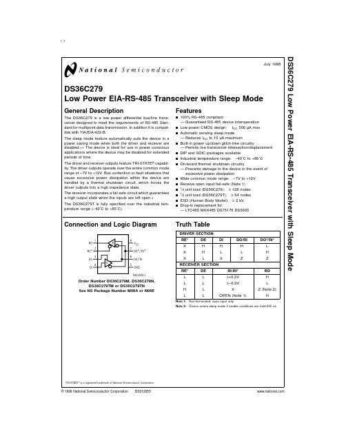
DS36C279Low Power EIA-RS-485Transceiver with Sleep ModeGeneral DescriptionThe DS36C279is a low power differential bus/line trans-ceiver designed to meet the requirements of RS-485Stan-dard for multipoint data transmission.In addition it is compat-ible with TIA/EIA-422-B.The sleep mode feature automatically puts the device in a power saving mode when both the driver and receiver are disabled.††The device is ideal for use in power conscious applications where the device may be disabled for extended periods of time.The driver and receiver outputs feature TRI-STATE ®capabil-ity.The driver outputs operate over the entire common mode range of −7V to +12V.Bus contention or fault situations that cause excessive power dissipation within the device are handled by a thermal shutdown circuit,which forces the driver outputs into a high impedance state.The receiver incorporates a fail safe circuit which guarantees a high output state when the inputs are left open.†The DS36C279T is fully specified over the industrial tem-perature range (−40˚C to +85˚C).Featuresn 100%RS-485compliant—Guaranteed RS-485device interoperation n Low power CMOS design:I CC 500µA max n Automatic sensing sleep mode—Reduces I CC to 10µA maximumn Built-in power up/down glitch-free circuitry—Permits live transceiver intersection/displacement n DIP and SOIC packages availablen Industrial temperature range:−40˚C to +85˚C n On-board thermal shutdown circuitry—Prevents damage to the device in the event of excessive power dissipationn Wide common mode range:−7V to +12V n Receive open input fail-safe (Note 1)n 1⁄4unit load (DS36C279):≥128nodes n 1⁄2unit load (DS36C279T):≥64nodes n ESD (Human Body Model):≥2kV n Drop-in replacement for:—LTC485MAX485DS75176DS3695Connection and Logic Diagram Truth TableDRIVER SECTION RE*DE DI DO/RI DO*/RI*X H H H L X H L L H X L XZZ RECEIVER SECTIONRE*DE RI-RI*RO L L ≥+0.2V H L L ≤−0.2V L H L XZ (Note 2)LLOPEN (Note 1)HNote 1:Non-terminated,open input onlyNote 2:Device enters sleep mode if enable conditions are held 600nsTRI-STATE ®is a registered trademark of National Semiconductor Corporation.DS012053-1Order Number DS36C279M,DS36C279N,DS36C279TM or DS36C279TNSee NS Package Number M08A or N08EJuly 1998DS36C279Low Power EIA-RS-485Transceiver with Sleep Mode©1999National Semiconductor Corporation Absolute Maximum Ratings(Note3)If Military/Aerospace specified devices are required, please contact the National Semiconductor Sales Office/ Distributors for availability and specifications.Supply Voltage(V CC)+12V Input Voltage(DE,RE*,&DI)−0.5V to(V CC+0.5V) Common Mode(V CM)Driver Output/Receiver Input±15V Input Voltage(DO/RI,DO*/RI*)±14V Receiver Output Voltage−0.5V to(V CC+0.5V) Maximum Package Power Dissipation@+25˚CM Package1190mW,derate9.5mW/˚C above+25˚C N Package744mW,derate 6.0mW/˚C above+25˚C Storage Temperature Range−65˚C to+150˚C Lead Temperature(Soldering4sec)+260˚C Recommended Operating ConditionsMin Typ Max Units Supply Voltage(V CC)+4.75+5.0+5.25V Bus Voltage−7+12V Operating Free Air Temperature(T A)DS36C279T−40+25+85˚C DS36C2790+25+70˚CElectrical Characteristics(Notes4,5)Over Supply Voltage and Operating Temperature ranges,unless otherwise specifiedSymbol Parameter Conditions Reference Min Typ Max Units DIFFERENTIAL DRIVER CHARACTERISTICSV OD1Differential Output Voltage I O=0mA(No Load)(422)(485)1.5 5.0VV OD0Output Voltage I O=0mA0 5.0V V OD0*Output Voltage(Output to GND)0 5.0V V OD2Differential Output Voltage R L=50Ω(422)Figure1 2.0 2.8V (Termination Load)R L=27Ω(485) 1.5 2.3 5.0V ∆V OD2Balance of V OD2R L=27Ωor50Ω(Note6)−0.20.1+0.2V |V OD2−V OD2*|(422,485)V OD3Differential Output Voltage R1=54Ω,R2=375ΩFigure2 1.5 2.0 5.0V (Full Load)V TEST=−7V to+12VV OC Driver Common Mode R L=27Ω(485)Figure10 3.0V Output Voltage R L=50Ω(422)0 3.0V ∆V OC Balance of V OC R L=27Ωor(Note6)−0.2+0.2V |V OC−V OC*|R L=50Ω(422,485)I OSD Driver Output Short-Circuit V O=+12V(485)Figure4200+250mACurrent V O=−7V(485)−190−250mA RECEIVER CHARACTERISTICSV TH Differential Input HighThreshold Voltage V O=V OH,I O=−0.4mA(Note7)(422,485)+0.035+0.2V −7V≤V CM≤+12VV TL Differential Input LowThreshold Voltage V O=V OL,I O=0.4mA−0.2−0.035V −7V≤V CM≤+12VV HST Hysteresis V CM=0V(Note8)70mV R IN Input Resistance−7V≤V CM≤+12V DS36C279T2468kΩDS36C2794868kΩI IN Line Input Current Other Input=0V,DS36C279V IN=+12V00.190.25mA(Note9)DE=V IL,RE*=V IL,V IN=−7V0−0.1−0.2mAV CC=4.75to5.25DS36C279T V IN=+12V00.190.5mAor0V V IN=−7V0−0.1−0.4mAI ING Line Input Current Glitch Other Input=0V,DE=V IL,RE*=V IL,DS36C279V IN=+12V00.190.25mA(Note9)V IN=−7V0−0.1−0.2mAV CC=+3.0V or0V, T A=25˚C DS36C279T V IN=+12V00.190.5mAV IN=−7V0−0.1−0.4mAI B Input Balance Test RS=500Ω(422)(Note12)±400mVV OH High Level Output Voltage I OH=−4mA,V ID=+0.2V ROFigure113.5 4.6VV OL Low Level Output Voltage I OL=+4mA,V ID=−0.2V0.30.5V 2Electrical Characteristics(Notes4,5)(Continued)Over Supply Voltage and Operating Temperature ranges,unless otherwise specifiedSymbol Parameter Conditions Reference Min Typ Max Units RECEIVER CHARACTERISTICSI OSR Short Circuit Current V O=GND RO73585mA I OZR TRI-STATE LeakageCurrentV O=0.4V to2.4V±1µA DEVICE CHARACTERISTICSV IH High Level Input Voltage DE,RE*,DI 2.0V CC VV IL Low Level Input Voltage GND0.8V I IH High Level Input Current V IH=V CC2µA I IL Low Level Input Current V CC=5V V IL=0V−2µAV CC=+3.0V−2µAI CC Power Supply Current(No Load)Driver and Receiver ONV CC200500µAI CCR Driver OFF,Receiver ON200500µA I CCD Driver ON,Receiver OFF200500µA I CCX Sleep Mode0.210µASwitching Characteristics(Notes5,10)Over Supply Voltage and Operating Temperature ranges,unless otherwise specifiedSymbol Parameter Conditions Reference Min Typ Max Units DRIVER CHARACTERISTICSt PHLD Differential PropagationDelay High to LowR L=54Ω,C L=100pFFigures5,6103980nst PLHD Differential PropagationDelay Low to High104080nst SKD Differential Skew0110ns |t PHLD−t PLHD|t r Rise Time32550ns t f Fall Time32550nst PHZ Disable Time High to Z C L=15pFRE*=L Figures7,880200nst PLZ Disable Time Low to Z Figures9,1080200nst PZH Enable Time Z to High C L=100pFRE*=L Figures7,850200nst PZL Enable Time Z to Low Figures9,1065200ns t PSH Driver Enable from Sleep C L=100pF Figures7,87098250ns Mode to Output High(Note11)t PSL Driver Enble from Sleep C L=100pF Figures9,107098250ns Mode to Output Low(Note11)RECEIVER CHARACTERISTICSt PHL Propagation Delay C L=15pF Figures12,1330210400ns High to Lowt PLH Propagation Delay30190400ns Low to Hight SK Skew,|t PHL−t PLH|02050nst PLZ Output Disable Time C L=15pFFigures14,15,1650150nst PHZ DE=H55150nst PZL Output Enable Time40150nst PZH45150nst PSH Receiver Enable from Sleep C L=15pF Figures14,167097250ns Mode to Output High(Note11)t PSL Receiver Enable from Sleep C L=15pF Figures14,157095250ns3Switching Characteristics (Notes 5,10)(Continued)Over Supply Voltage and Operating Temperature ranges,unless otherwise specifiedSymbolParameterConditions ReferenceMinTypMaxUnitsRECEIVER CHARACTERISTICSMode to Output Low(Note 11)Note 3:“Absolute Maximum Ratings”are those values beyond which the safety of the device cannot be guaranteed.They are not meant to imply that the devices should be operated at these limits.The table of “Electrical Characteristics”specifies conditions of device operation.Note 4:Current into device pins is defined as positive.Current out of device pins is defined as negative.All voltages are referenced to ground except V OD1and V OD2.Note 5:All typicals are given for:V CC =+5.0V,T A =+25˚C.Note 6:Delta |V OD2|and Delta |V OC |are changes in magnitude of V OD2and V OC ,respectively,that occur when input changes state.Note 7:Threshold parameter limits specified as an algebraic value rather than by magnitude.Note 8:Hysteresis defined as V HST =V TH −V TL .Note 9:I IN includes the receiver input current and driver TRI-STATE leakage current.Note 10:C L includes probe and jig capacitance.Note 11:For enable from sleep mode delays DE =L and RE*=H for greater than 600ns prior to test (device is in sleep mode).Note 12:For complete details of test,see RS-485.Parameter Measurement InformationDS012053-2FIGURE 1.Driver V OD2and V OCDS012053-17FIGURE 2.Driver V OD3DS012053-3FIGURE 3.Driver V OH and V OLDS012053-4Vtest =−7V to +12VFIGURE 4.Driver I OSDDS012053-5FIGURE 5.Driver Differential Propagation Delay Test Circuit 4Parameter Measurement Information(Continued)DS012053-6FIGURE6.Driver Differential Propagation Delays and Differential Rise and Fall TimesDS012053-7FIGURE7.TRI-STATE and Sleep Mode Test Circuit(t PZH,(t PSH),t PHZ)DS012053-8FIGURE8.TRI-STATE and Sleep Mode Waveforms(t PZH,(t PSH),t PHZ)DS012053-9FIGURE9.TRI-STATE and Sleep Mode Test Circuit(t PZL,(t PSL),t PLZ)DS012053-10FIGURE10.TRI-STATE and Sleep Mode Waveforms(t PZL,(t PSL),t PLZ)DS012053-11FIGURE11.Receiver V OH and V OLDS012053-12FIGURE12.Receiver Differential Propagation DelayTest Circuit5Parameter Measurement Information(Continued)DS012053-13FIGURE13.Receiver Differential Propagation Delay WaveformsDS012053-14FIGURE14.Receiver TRI-STATE and Sleep Mode Test CircuitDS012053-15FIGURE15.Receiver Enable and Disable Waveforms(t PLZ,t PZL,(t PSL))DS012053-16FIGURE16.Receiver Enable and Disable Waveforms(t PHZ,t PZH,(t PSH)) 6Parameter Measurement Information(Continued)Typical Application InformationTABLE 1.Device Pin DescriptionsPin Description1ROReceiver Output:When RE (Receiver Enable)is LOW,the receiver is enabled (ON),if DO/RI ≥DO*/RI*by 200mV,RO will be HIGH.If DO/RI ≤DO*/RI*by 200mV,RO will be LOW.Additionally RO will be HIGH for OPEN (Non-terminated)Inputs.2RE*Receiver Output Enable:When RE*is LOW the receiver output is enabled.When RE*is HIGH,the receiver output is in TRI-STATE (OFF).When RE*is HIGH and DE is LOW,the device will enter a low-current sleep mode after 600ns.3DEDriver Output Enable:When DE is HIGH,the driver outputs are enabled.When DE is LOW,the driver outputs are in TRI-STATE (OFF).When RE*is HIGH and DE is LOW,the device will enter a low-current sleep mode after 600ns.4DI Driver Input:When DE (Driver Enable)is HIGH,the driver is enabled,if DI is LOW,then DO/RI will be LOW and DO*/RI*will be HIGH.If DI is HIGH,then DO/RI is HIGH and DO*/RI*is LOW.5GND Ground Connection.6DO/RI Driver Output/Receiver Input,485Bus Pin.7DO*/RI*Driver Output/Receiver Input,485Bus Pin.8V CCPositive Power Supply Connection:Recommended operating range for V CC is +4.75V to +5.25V.Unit LoadA unit load for an RS-485receiver is defined by the input cur-rent versus the input voltage curve.The gray shaded region is the defined operating range from −7V to +12V.The top border extending from −3V at 0mA to +12V at +1mA is de-fined as one unit load.Likewise,the bottom border extending from +5V at 0mA to −7V at −0.8mA is also defined as oneunit load (see Figure 19).An RS-485driver is capable of driving up to 32unit loads.This allows up to 32nodes on a single bus.Although sufficient for many applications,it is sometimes desirable to have even more nodes.For ex-ample,an aircraft that has 32rows with 4seats per row would benefit from having 128nodes on one bus.This wouldDS012053-19FIGURE 17.Entering Sleep Mode ConditionsDS012053-18FIGURE 18.Typical RS-485Bus Interface7Unit Load(Continued)allow signals to be transferred to and from each individual seat to1main ually there is one or two less seats in the last row of the aircraft near the restrooms and food storage area.This frees the node for the main station.The DS36C278,the DS36C279,and the DS36C280all have 1⁄2unit load and1⁄4unit load(UL)options available.These devices will allow up to64nodes or128nodes guaranteed over temperature depending upon which option is selected. The1⁄2UL option is available in industrial temperature and the1⁄4UL is available in commercial temperature.First,for a1⁄2UL device the top and bottom borders shown in Figure19are scaled.Both0mA reference points at+5V and −3V stay the same.The other reference points are+12V at +0.5mA for the top border and−7V at−0.4mA for the bot-tom border(see Figure19).Second,for a1⁄4UL device the top and bottom borders shown in Figure19are scaled also. Again,both0mA reference points at+5V and−3V stay the same.The other reference points are+12V at+0.25mA for the top border and−7V at−0.2mA for the bottom border (see Figure19).The advantage of the1⁄2UL and1⁄4UL devices is the in-creased number of nodes on one bus.In a single master multi-slave type of application where the number of slaves exceeds32,the DS36C278/279/280may save in the cost of extra devices like repeaters,extra media like cable,and/or extra components like resistors.The DS36C279and DS36C280have an additional feature which offers more advantages.The DS36C279has an auto-matic sleep mode function for power conscious applications. The DS36C280has a slew rate control for EMI conscious applications.Refer to the sleep mode and slew rate control portion of the application information section in the corre-sponding datasheet for more information on these features. Sleep ModeThe DS36C279features an automatic shutdown mode that allows the device to save power when not transmitting data. Since the shutdown mode is automatic,no external compo-nents are required.It may be used as little or as much as the application requires.The more the feature is utilized,the more power it saves.The sleep mode is automatically entered when both the driver and receiver are disabled.This occurs when both the DE pin is asserted to a logic low and the RE*pin is asserted to a logic high.Once both pins are asserted the device will enter sleep mode typically in50ns.The DS36C279is guar-anteed to go into sleep mode within600ns after both pins are asserted.The device wakes up(comes out of sleep mode)when either the DE pin is asserted to a logic high and/or the RE*pin is asserted to a logic low.After the device enters sleep mode it will take longer for the device to wake up than it does for the device to enable from TRI-STATE.Re-fer to datasheet specifications t PSL and t PSH and compare with t PZL and t PZH for timing differences.The benefit of the DS36C279is definitely its power savings. When active the device has a maximum I CC of500µA. When in sleep mode the device has a maximum I CC of only 10µA,which is50times less power than when active.The I CC when the device is active is already very low but when in sleep mode the I CC is ultra low.DS012053-20 FIGURE19.Input Current vs Input VoltageOperating Range8Physical Dimensions inches(millimeters)unless otherwise noted8-Lead(0.150"Wide)Molded Small Outline Package,JEDECOrder Number DS36C279M or DS36C279TMNS Package Number M08A8-Lead(0.300"Wide)Molded Dual-In-Line PackageOrder Number DS36C279N or DS36C279TNNS Package Number N08E9LIFE SUPPORT POLICYNATIONAL’S PRODUCTS ARE NOT AUTHORIZED FOR USE AS CRITICAL COMPONENTS IN LIFE SUPPORT DE-VICES OR SYSTEMS WITHOUT THE EXPRESS WRITTEN APPROVAL OF THE PRESIDENT OF NATIONAL SEMI-CONDUCTOR CORPORATION.As used herein:1.Life support devices or systems are devices or sys-tems which,(a)are intended for surgical implant intothe body,or (b)support or sustain life,and whose fail-ure to perform when properly used in accordancewith instructions for use provided in the labeling,can be reasonably expected to result in a significant injury to the user.2.A critical component is any component of a life support device or system whose failure to perform can be rea-sonably expected to cause the failure of the life support device or system,or to affect its safety or effectiveness.National Semiconductor Corporation AmericasTel:1-800-272-9959Fax:1-800-737-7018Email:support@National Semiconductor EuropeFax:+49(0)180-5308586Email:europe.support@Deutsch Tel:+49(0)180-5308585English Tel:+49(0)180-5327832Français Tel:+49(0)180-5329358Italiano Tel:+49(0)180-5341680National Semiconductor Asia Pacific Customer Response Group Tel:65-2544466Fax:65-2504466Email:sea.support@National Semiconductor Japan Ltd.Tel:81-3-5639-7560Fax:81-3-5639-7507D S 36C 279L o w P o w e rE I A -R S -485T r a n s c e i v e r w i t h S l e e p M o d eNational does not assume any responsibility for use of any circuitry described,no circuit patent licenses are implied and National reserves the right at any time without notice to change said circuitry and specifications.。
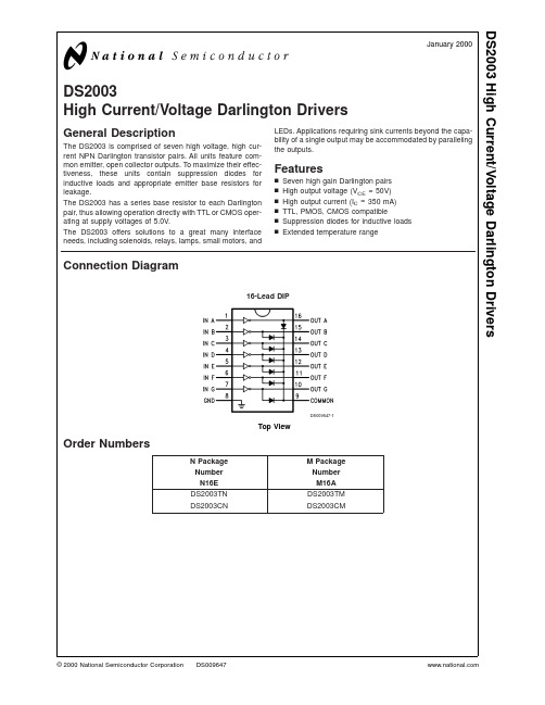
DS2003High Current/Voltage Darlington DriversGeneral DescriptionThe DS2003is comprised of seven high voltage,high cur-rent NPN Darlington transistor pairs.All units feature com-mon emitter,open collector outputs.To maximize their effec-tiveness,these units contain suppression diodes for inductive loads and appropriate emitter base resistors for leakage.The DS2003has a series base resistor to each Darlington pair,thus allowing operation directly with TTL or CMOS oper-ating at supply voltages of 5.0V.The DS2003offers solutions to a great many interface needs,including solenoids,relays,lamps,small motors,andLEDs.Applications requiring sink currents beyond the capa-bility of a single output may be accommodated by paralleling the outputs.Featuresn Seven high gain Darlington pairs n High output voltage (V CE =50V)n High output current (I C =350mA)n TTL,PMOS,CMOS compatiblen Suppression diodes for inductive loads nExtended temperature rangeConnection DiagramOrder NumbersN Package Number N16E M Package Number M16A DS2003TN DS2003TM DS2003CNDS2003CM16-Lead DIPDS009647-1Top ViewJanuary 2000DS2003High Current/Voltage Darlington Drivers©2000National Semiconductor Corporation Absolute Maximum Ratings (Note 1)If Military/Aerospace specified devices are required,please contact the National Semiconductor Sales Office/Distributors for availability and specifications.Storage Temperature Range −65˚C to +150˚C Operating Temperature RangeDS2003TN,DS2003TM −40˚C to +105˚CDS2003CN,DS2003CM 0˚C to +85˚CLead TemperatureSoldering,10seconds 265˚CMaximum Power Dissipation *at T A =25˚CN16E Package 1330mW M16A Package 770mWInput Voltage 30V Output Voltage55V Emitter-Base Voltage6.0V Continuous Collector Current 500mA Continuous Base Current 25mANote:*Derate N16E package 13.3mW/˚C for T A above 25˚C.Derate M16Apackage 7.7mW/˚C for T A above 25˚C.Electrical CharacteristicsT A =25˚C,unless otherwise specified (Note 2)Symbol Parameter ConditionsMinTypMax UnitsI CEXOutput Leakage CurrentT A =25˚C,V CE =50V (Figure 1)20T A =85˚C,V CE =50V (Figure 1)for DS2003CN,DS2003CM 100µA T A =105˚C,V CE =50V (Figure 1)for DS2003TN,DS2003TM 150V CE(Sat)Collector-Emitter Saturation Voltage I C =350mA,I B =500µA (Figure 3)(Note 3) 1.25 1.6V I C =200mA,I B =350µA (Figure 3) 1.1 1.3I C =100mA,I B =250µA (Figure 3)0.9 1.1I I(ON)Input Current V I =3.85V (Figure 4)0.93 1.35mA I I(OFF)Input Current (Note 4)T A =85˚C for DS2003CN,DS2003CM I C =500µA (Figure 5)50100µA V I(ON)Input Voltage (Note 5)V CE =2.0V,I C =200mA (Figure 6) 2.4VV CE =2.0V,I C =250mA (Figure 6) 2.7V CE =2.0V,I C =300mA (Figure 6)3.0C I Input Capacitance 1530pF t PLH Turn-On Delay 0.5V I to 0.5V O1.0µs t PHL Turn-Off Delay 0.5V I to 0.5V O1.0µs I R Clamp Diode Leakage Current V R =50V (Figure 7)T A =25˚C 50µA T A =85˚C100µA V FClamp Diode Forward VoltageI F =350mA (Figure 8)1.72.0V Note 1:“Absolute Maximum Ratings”are those values beyond which the safety of the device cannot be guaranteed.They are not meant to imply that the devices should be operated at these limits.The tables of “Electrical Characteristics”provide conditions for actual device operation.Note 2:All limits apply to the complete Darlington series except as specified for a single device type.Note 3:Under normal operating conditions these units will sustain 350mA per output with V CE (Sat)=1.6V at 70˚C with a pulse width of 20ms and a duty cycle of 30%.Note 4:The I I(OFF)current limit guaranteed against partial turn-on of the output.Note 5:The V I(ON)voltage limit guarantees a minimum output sink current per the specified test conditions.D S 2003 2Typical Performance CharacteristicsEquivalent CircuitsCollector Current vs Saturation VoltageDS009647-18Collector Current vs Input CurrentDS009647-19Input Current vs Input VoltageDS009647-20Peak Collector Current vs Duty Cycle and Number of Outputs (Molded Package)DS009647-22Peak Collector Current vs Duty Cycle and Number of Outputs (Ceramic Package)DS009647-23DS009647-3DS20033Test CircuitsDS009647-7FIGURE 1.DS009647-8FIGURE 2.DS009647-9FIGURE 3.DS009647-10FIGURE 4.DS009647-11FIGURE 5.DS009647-12FIGURE 6.DS009647-13FIGURE 7.DS009647-14FIGURE 8.D S 2003 4Physical Dimensionsinches (millimeters)unless otherwise notedSurface Mount Package (M)Order Number DS2003CM,DS2003TMNS Package Number M16AMolded Dual-In-Line Package (N)Order Number DS2003CN,DS2003TNNS Package Number N16EDS20035NotesLIFE SUPPORT POLICYNATIONAL’S PRODUCTS ARE NOT AUTHORIZED FOR USE AS CRITICAL COMPONENTS IN LIFE SUPPORT DEVICES OR SYSTEMS WITHOUT THE EXPRESS WRITTEN APPROVAL OF THE PRESIDENT AND GENERAL COUNSEL OF NATIONAL SEMICONDUCTOR CORPORATION.As used herein:1.Life support devices or systems are devices or systems which,(a)are intended for surgical implant into the body,or (b)support or sustain life,and whose failure to perform when properly used in accordance with instructions for use provided in the labeling,can be reasonably expected to result in a significant injury to the user.2.A critical component is any component of a life support device or system whose failure to perform can be reasonably expected to cause the failure of the life support device or system,or to affect its safety or effectiveness.National Semiconductor Corporation AmericasTel:1-800-272-9959Fax:1-800-737-7018Email:support@National Semiconductor EuropeFax:+49(0)180-5308586Email:europe.support@Deutsch Tel:+49(0)180-5308585English Tel:+49(0)180-5327832Français Tel:+49(0)180-5329358Italiano Tel:+49(0)180-5341680National Semiconductor Asia Pacific Customer Response Group Tel:65-2544466Fax:65-2504466Email:sea.support@National Semiconductor Japan Ltd.Tel:81-3-5639-7560Fax:81-3-5639-7507D S 2003H i g h C u r r e n t /V o l t a g e D a r l i n g t o n D r i v e r sNational does not assume any responsibility for use of any circuitry described,no circuit patent licenses are implied and National reserves the right at any time without notice to change said circuitry and specifications.。

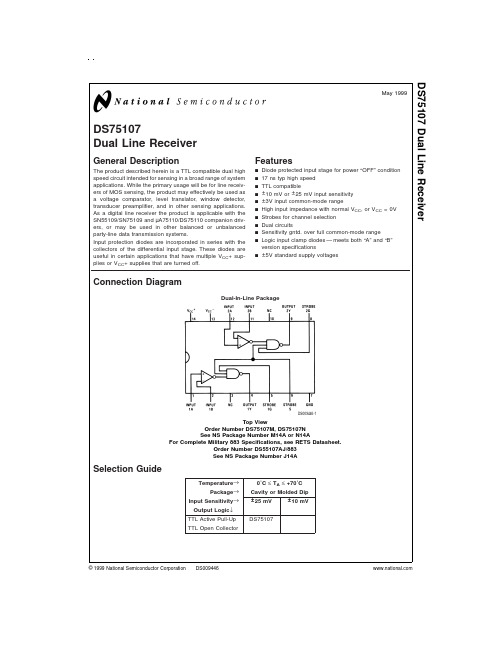
DS75107Dual Line ReceiverGeneral DescriptionThe product described herein is a TTL compatible dual high speed circuit intended for sensing in a broad range of system applications.While the primary usage will be for line receiv-ers of MOS sensing,the product may effectively be used as a voltage comparator,level translator,window detector,transducer preamplifier,and in other sensing applications.As a digital line receiver the product is applicable with the SN55109/SN75109and µA75110/DS75110companion driv-ers,or may be used in other balanced or unbalanced party-line data transmission systems.Input protection diodes are incorporated in series with the collectors of the differential input stage.These diodes are useful in certain applications that have multiple V CC +sup-plies or V CC +supplies that are turned off.Featuresn Diode protected input stage for power “OFF”condition n 17ns typ high speed n TTL compatiblen ±10mV or ±25mV input sensitivity n ±3V input common-mode rangen High input impedance with normal V CC ,or V CC =0V n Strobes for channel selection n Dual circuitsn Sensitivity gntd.over full common-mode rangenLogic input clamp diodes —meets both “A”and “B”version specificationsn ±5V standard supply voltagesConnection DiagramSelection GuideTemperature →0˚C ≤T A ≤+70˚C Package →Cavity or Molded DipInput Sensitivity →±25mV ±10mVOutput Logic ↓TTL Active Pull-Up DS75107TTL Open CollectorDual-In-Line PackageDS009446-1Top ViewOrder Number DS75107M,DS75107N See NS Package Number M14A or N14AFor Complete Military 883Specifications,see RETS Datasheet.Order Number DS55107AJ/883See NS Package Number J14AMay 1999DS75107Dual Line Receiver©1999National Semiconductor Corporation Absolute Maximum Ratings(Note1)If Military/Aerospace specified devices are required, please contact the National Semiconductor Sales Office/ Distributors for availability and specifications.Supply Voltage,V CC+7V Supply Voltage,V CC−−7V Differential Input Voltage±6V Common Mode Input Voltage±5V Strobe Input Voltage 5.5V Storage Temperature Range−65˚C to+150˚C Maximum Power Dissipation(Note1)at25˚CCavity Package1308mW Molded Package1207mW Lead Temperature(Soldering,4sec)260˚C Note:Derate cavity package8.7mW/˚C above25˚C;derate molded package9.7mW/˚C above25˚C.Operating ConditionsDS75107Min Nom Max Supply Voltage V CC+ 4.75V5V 5.25VSupply Voltage V CC−−4.75V−5V−5.25VOperating Temperature Range0˚C to+70˚CDS75107Electrical CharacteristicsT MIN≤T A≤T MAX(Notes2,3)Symbol Parameter Conditions Min Typ Max Units I IH High Level Input Current V CC+=Max,V CC−=Max,3075µA into A1,B1,A2or B2V ID=0.5V,V IC=−3V to3VI IL Low Level Input Current V CC+=Max,V CC−=Max,−10µA into A1,B1,A2or B2V ID=−2V,V IC=−3V to3VI IH High Level Input Current V CC+=Max,V IH(S)=2.4V40µAinto G1or G2V CC−=Max V IH(S)Max V CC+1mA I IL Low Level Input Current V CC+=Max,V CC−=Max,−1.6mA into G1or G2V IL(S)=0.4VI IH High Level Input Current into S V CC+=Max,V IH(S)=2.4V80µAV CC−=Max V IH(S)=Max V CC+2mA I IL Low Level Input Current into S V CC+=Max,V CC−=Max,−3.2mAV IL(S)=0.4VV OH High Level Output Voltage V CC+=Min,V CC−=Min,I LOAD=−400µA,V ID=25mV, 2.4VV IC=−3V to3V,(Note3)V OL Low Level Output Voltage V CC+=Min,V CC−=Min,I SINK=16mA,V ID=−25mV,0.4VV IC=−3V to3VI OH High Level Output Current V CC+=Min,V CC−=Min250µAV OH=Max V CC+I OS Short Circuit Output Current V CC+=Max,V CC−=Max,−18−70mA(Notes3,5)I CCH+High Logic Level Supply V CC+=Max,V CC−=Max,1830mA Current from V CC V ID=25mV,T A=25˚CI CCH−High Logic Level Supply V CC+=Max,V CC−=Max,−8.4−15mA Current from V CC V ID=25mV,T A=25˚CV I Input Clamp Voltage on G or S V CC+=Min,V CC−=Min,−1−1.5VI IN=−12mA,T A=25˚C2Switching CharacteristicsV CC+=5V,V CC−=−5V,T A=25˚CSymbol Parameter Conditions Min Typ Max Unitst PLH(D)Propagation Delay Time,Low toHigh Level,from Differential InputsA andB to Output R L=390Ω,C L=50pF,(Note4)1725ns1925nst PHL(D)Propagation Delay Time,High toLow Level,from Differential InputsA andB to Output R L=390Ω,C L=50pF,(Note4)1725ns1925nst PLH(S)Propagation Delay Time,Low toHigh Level,from Strobe Input G orS to Output R L=390Ω,C L=50pF1015ns1320nst PHL(S)Propagation Delay Time,High toLow Level,from Strobe Input G orS to Output R L=390Ω,C L=50pF815ns1320nsSwitching CharacteristicsV CC+=5V,V CC−=−5V,T A=25˚CSymbol Parameter Conditions Min Typ Max Unitst PLH(D)Propagation Delay Time,Low-to-R L=470Ω,C L=15pF,(Note6)High Level,from Differential35nsInputs A and B to Outputt PHL(D)Propagation Delay Time,High-to-R L=470Ω,C L=15pF,(Note6)Low Level,from Differential20nsInputs A and B to Outputt PLH(S)Propagation Delay Time,Low-to-R L=470Ω,C L=15pFHigh Level,from Strobe Input G17nsor S to Outputt PHL(S)Propagation Delay Time,High-to-R L=470Ω,C L=15pFLow Level,from Strobe Input G17nsor S to OutputNote1:“Absolute Maximum Ratings”are those values beyond which the safety of the device cannot be guaranteed.Except for“Operating Temperature Range”theyare not meant to imply that the devices should be operated at these limits.The table of“Electrical Characteristics”provides conditions for actual device operation. Note2:Unless otherwise specified min/max limits apply across the0˚C to+70˚C range for the DS75107.All typical values are for T A=25˚C and V CC=5V.Note3:All currents into device pins shown as positive,out of device pins as negative,all voltages referenced to ground unless otherwise noted.All values shownas max or min on absolute value basis.Note4:Differential input is+100mV to−100mV pulse.Delays read from0mV on input to1.5V on output.Note5:Only one output at a time should be shorted.Note6:Differential input is+10mV to−30mV pulse.Delays read from0mV on input to1.5V on output.Voltage WaveformsDS009446-123Typical ApplicationsAPPLICATIONThe DS75107dual line circuit is designed specifically for use in high speed data transmission systems that utilize bal-anced,terminated transmission lines such as twisted-pair lines.The system operates in the balanced mode,so that noise induced on one line is also induced on the other.The noise appears common mode at the receiver input terminals where it is rejected.The ground connection between the line driver and receiver is not part of the signal circuit so that sys-tem performance is not affected by circulating ground cur-rents.The unique driver output circuit allows terminated transmis-sion lines to be driven at normal line impedances.High speed system operation is ensured since line reflections are virtually eliminated when terminated lines are used.Cross-talk is minimized by low signal amplitudes and low line impedances.The typical data delay in a system is approximately (30+1.3L)ns,where L is the distance in feet separating the driver and receiver.This delay includes one gate delay in both the driver and receiver.Data is impressed on the balanced-line system by unbalanc-ing the line voltages with the driver output current.The driven line is selected by appropriate driver input logic levels.The voltage difference is approximately:V DIFF ≅1⁄2I O(on)x R T :(1)High series line resistance will cause degradation of the sig-nal.The receivers,however,will detect signals as low as 25mV(or less).For normal line resistances,data may be re-covered from lines of several thousand feet in length.Line termination resistors (R T )are required only at the ex-treme ends of the line.For short lines,termination resistors at the receiver only may prove adequate.The signal ampli-tude will then be approximately:V DIFF ≅I O(on)x R T :(2)Data-Bus or Party-Line SystemDS009446-2Data-Bus or Party-Line SystemDS009446-3 4Typical Applications(Continued)The strobe feature of the receiver and the inhibit feature ofthe driver allows the DS75107dual line circuit to be used indata-bus or party-line systems.In these applications,severaldrivers and receivers may share a common transmissionline.An enabled driver transmits data to all enabled receiv-ers on the line while other drivers and receivers are disabled.Data is thus time multiplexed on the transmission line.DS75107device specifications allow widely varying thermaland electrical environments at the various driver and re-ceiver locations.The data-bus system offers maximum per-formance at minimum cost.The DS75107dual line circuits may also be used in unbal-anced or single line systems.Although these systems do notoffer the same performance as balanced systems for longlines,they are adequate for very short lines where environ-ment noise is not severe.The receiver threshold level is established by applying a DCreference voltage to one receiver input terminal.The signalfrom the transmission line is applied to the remaining input.The reference voltage should be optimized so that signalswing is symmetrical about it for maximum noise margin.The reference voltage should be in the range of−3.0V to+3.0V.It can be provided by a voltage supply or by a voltagedivider from an available supply voltage.Precautions in the Use of DS1603,DS3603,DS55107,DS75107,DS75108and DS75208Dual Line ReceiversThe following precaution should be observed when using ortesting DS75107line circuits.When only one receiver in a package is being used,at leastone of the differential inputs of the unused receiver shouldbe terminated at some voltage between−3.0V and+3.0V,preferably at ground.Failure to do so will cause improper op-eration of the unit being used because of common bias cir-cuitry for the current sources of the two receivers.The DS75107line receiver features a common mode inputvoltage range of±3.0V.This satisfies the requirements for allbut the noisiest system applications.For these severe noiseenvironments,the common mode range can be extended bythe use of external input mon mode inputvoltages can in this way be reduced to±3.0V at the receiverinput terminals.Differential data signals will be reduced pro-portionately.Input sensitivity,input impedance and delaytimes will be adversely affected.Circuit Differences Between“A”and Standard DevicesThe difference between the“A”and standard devices isshown in the following schematics of the input stage.Unbalanced or Single-Line SystemsDS009446-4Increasing Common Mode InputVoltage Range of ReceiverDS009446-5DS75108Wired-OR Output ConnectionsDS009446-6“A”DevicesDS009446-75Typical Applications(Continued)The input protection diodes are useful in certain party-linesystems which may have multiple V+power supplies and,inwhich case,may be operated with some of the V+suppliesturned off.In such a system,if a supply is turned off and al-lowed to go to ground,the equivalent input circuit connectedto that supply would be as follows:This would be a problem in specific systems which mightpossibly have the transmission lines biased to some poten-tial greater than1.4V.Since this is not a widespread applica-tion problem,both the“A”and standard devices will be avail-able.The ratings and characteristic specifications of the“A”devices are the same as those of the standard devices.Standard DevicesDS009446-8“A”DevicesDS009446-9Standard DevicesDS009446-106Schematic DiagramsDS55107/DS75107,DS75108,DS75208DS009446-111⁄2of the dual circuit is shown.*Indicates connections common to second half of dual circuit.Components shown with dash lines are applicable to the DS55107,DS75207and DS75107only.7Physical Dimensions inches(millimeters)unless otherwise notedCeramic Dual-In-Line Package(J)Order Number DS75107JNS Package Number J14AMolded Dual-In-Line Package(M)Order Number DS75107M,DS75107AMNS Package Number M14A 8Physical Dimensions inches(millimeters)unless otherwise noted(Continued)LIFE SUPPORT POLICYNATIONAL’S PRODUCTS ARE NOT AUTHORIZED FOR USE AS CRITICAL COMPONENTS IN LIFE SUPPORT DEVICES OR SYSTEMS WITHOUT THE EXPRESS WRITTEN APPROVAL OF THE PRESIDENT AND GENERAL COUNSEL OF NATIONAL SEMICONDUCTOR CORPORATION.As used herein:1.Life support devices or systems are devices orsystems which,(a)are intended for surgical implantinto the body,or(b)support or sustain life,andwhose failure to perform when properly used inaccordance with instructions for use provided in thelabeling,can be reasonably expected to result in asignificant injury to the user.2.A critical component is any component of a lifesupport device or system whose failure to performcan be reasonably expected to cause the failure ofthe life support device or system,or to affect itssafety or effectiveness.National SemiconductorCorporationAmericasTel:1-800-272-9959Fax:1-800-737-7018Email:support@National SemiconductorEuropeFax:+49(0)180-5308586Email:europe.support@Deutsch Tel:+49(0)180-5308585English Tel:+49(0)180-5327832Français Tel:+49(0)180-5329358Italiano Tel:+49(0)180-5341680National SemiconductorAsia Pacific CustomerResponse GroupTel:65-2544466Fax:65-2504466Email:sea.support@National SemiconductorJapan Ltd.Tel:81-3-5639-7560Fax:81-3-5639-7507 Molded Dual-In-Line Package(N)Order Number DS75107N,DS75107ANNS Package Number N14ADS75107DualLineReceiver National does not assume any responsibility for use of any circuitry described,no circuit patent licenses are implied and National reserves the right at any time without notice to change said circuitry and specifications.。
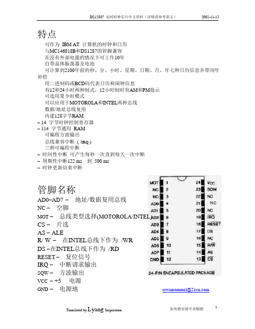
可作为IBM AT 计算机的时钟和日历与MC146818B和DS1287的管脚兼容在没有外部电源的情况下可工作10年自带晶体振荡器及电池可计算到2100年前的秒、分、小时、星期、日期、月、年七种日历信息并带闰年补偿用二进制码或BCD码代表日历和闹钟信息有12和24小时两种制式,12小时制时有AM和PM提示可选用夏令时模式可以应用于MOTOROLA和INTEL两种总线数据/地址总线复用内建128字节RAM– 14 字节时钟控制寄存器– 114 字节通用RAM可编程方波输出总线兼容中断( /IRQ )三种可编程中断–时间性中断可产生每秒一次直到每天一次中断–周期性中断122 ms 到500 ms–时钟更新结束中断管脚名称AD0–AD7 –地址/数据复用总线NC –空脚MOT –总线类型选择(MOTOROLA/INTEL)CS –片选AS – ALER/ W –在INTEL总线下作为/WRDS –在INTEL总线下作为/RDRESET –复位信号IRQ –中断请求输出SQW –方波输出VCC – +5 电源GND –电源地erwinrommel@图1为DS12887的结构框图上电/掉电当VCC高于4.25V 200ms后,芯片可以被外部程序操作;当VCC低于4.25V时,芯片处于写保护状态(所有的输入均无效),同时所有输出呈高阻状态;当VCC低于3V 时,芯片将自动把供电方式切换为由内部电池供电。
管脚功能MOT (总线模式选择)当此脚接到V CC 时,选用的是MOTOROLA总线时序;当它接到地或不接时,选用的是INTEL总线时序。
SQW (方波输出) –当VCC低于4.25V时没有作用。
周期性中断率和方波中断频率表 1AD0–AD7 (双向数据/地址复用总线)AS (地址锁存)–ALEDS (Data Strobe or Read Input)–RD当系统选择的是INTEL总线模式时,DS被称作RD。
**-20**表格填写指南和确认在递交美国领事或移民官员之前,请阅读该页内容并在第一页交流访问者确认处签名。
1.我明了以下条款是适用于交流访问者:(a)两年美国国外居住要求(《移民与国籍法》修正案第212(e)章节和94至484页):规定:直接或间接的受本国政府或美国政府全部或部分资助的项目的交流访问者要求在项目结束后回原居住国居住两年,才有资格获准移民、临时工或跨国公司调派人员身份。
同样的,如果交换访问者获得某项其本国紧缺的技术(这些技能列明在“交流访问者技术名单”),他们将受回原居住国两年居住要求限制。
这个规定也适用于进入美国接受研究生医学教育或培训的外籍医生。
就212(e)条款,美国国务院保留最终决定权。
注:与美国公民结婚、或合法永久居民、或在美国生产均不免除这项规定。
(b)居留延期/项目变更:为申请项目期延长或项目变更,必须从资助方获得或由资助方协助获取完整的DS-2019表。
(c)居留限制:学生-只要是学习全日制学位课程,或如果保证在全日制非学位项目学习达24个月;资助方推荐的也许获准在获得学位或学历后允许再停留18个月的学术培训;经资助方批准的为期不超过36个月的博士后学术培训。
中学生-长达1学年;培训生-18个月;飞行培训生-24个月;教师、教授和研究学者-3年;短期学者-6个月;专家-1年;国际访问者-1年;外籍医生-如果美国国务院批准,可获得延期不超过7年的完成医学专业所需的时间;政府访客-长达18个月;令营辅导员-达4个月;暑期旅行/工作者-达4个月;互惠生-1年;实习生-达12个月。
(d)入学所需文件/重新接纳作为交换访问者:为合格进入美国,交流访问者必须在入境港出示如下材料:(1)有效的非移民签证,获得豁免除外;(2)扣除预期的入境期后有效期至少6个月的有效护照,获得豁免除外;(3)为在先前审定的停留期内往返美国,真实有效的DS-2019表格(带2-D条形码)必须由交流访问者保存,在如该表所示的项目限期内(见该表第1页第3条),交流访问者被允许保留居留身份出美旅游。
DS8922/DS8922A/DS8923A TRI-STATE ®RS-422Dual Differential Line Driver and Receiver PairsGeneral DescriptionThe DS8922/22A and DS8923A are Dual Differential Line Driver and Receiver pairs.These devices are designed spe-cifically for applications meeting the ST506,ST412and ESDI Disk Drive Standards.In addition,the devices meet the requirements of the EIA Standard RS-422.These devices offer an input sensitivity of 200mV over a ±7V common mode operating range.Hysteresis is incorpo-rated (typically 70mV)to improve noise margin for slowly changing input waveforms.An input fail-safe circuit is pro-vided such that if the receiver inputs are open the output assumes the logical one state.The DS8922A and DS8923A drivers are designed to provide unipolar differential drive to twisted pair or parallel wire trans-mission plementary outputs are logically ANDed and provide an output skew of 0.5ns (typ.)with propagation delays of 12ns.Both devices feature TRI-STATE outputs.The DS8922/22A have independent control functions common to a driver and receiver pair.The DS8923A has separate driver and receiver control functions.Power up/down circuitry is featured which will TRI-STATE the outputs and prevent erroneous glitches on the transmis-sion lines during system power up or power down operation.The DS8922/22A and DS8923A are designed to be compat-ible with TTL and CMOS.Featuresn 12ns typical propagation delay n Output skew —±0.5ns typicaln Meets the requirements of EIA Standard RS-422n Complementary Driver Outputsn High differential or common-mode input voltage ranges of ±7Vn ±0.2V receiver sensitivity over the input voltage range n Receiver input fail-safe circuitryn Receiver input hysteresis —70mV typical n Glitch free power up/down nTRI-STATE outputsConnection DiagramsDS8922A Dual-In-Line00851101Order Number DS8922M,DS8922N,DS8922AM or DS8922ANSee NS Package Number M16A or N16ETRI-STATE ®is a registered trademark of National Semiconductor Corp.July 2004DS8922/DS8922A/DS8923A TRI-STATE RS-422Dual Differential Line Driver and Receiver Pairs©2004National Semiconductor Corporation Connection Diagrams(Continued)DS8923A Dual-In-Line00851102Order Number DS8923AM,DS8923AN,See NS Package Number M16A or N16EDS8922/22AEN1EN2RO1RO2DO1DO200ACTIVE ACTIVE ACTIVE ACTIVE 10HI-Z ACTIVE HI-Z ACTIVE 01ACTIVE HI-Z ACTIVE HI-Z 11HI-ZHI-Z HI-ZHI-ZDS8923ADEN REN RO1RO2DO1DO200ACTIVE ACTIVE ACTIVE ACTIVE 10ACTIVE ACTIVE HI-Z HI-Z 01HI-Z HI-Z ACTIVE ACTIVE 11HI-ZHI-ZHI-ZHI-ZD S 8922/D S 8922A /D S 8923A 2Absolute Maximum Ratings(Note1)If Military/Aerospace specified devices are required, please contact the National Semiconductor Sales Office/ Distributors for availability and specifications.Supply Voltage7V Drive Input Voltage−0.5V to+7V Output Voltage 5.5V Receiver Output Sink Current50mA Receiver Input Voltage±10V Differential Input Voltage±12V Maximum Package Power Dissipation@+25˚CM Package1300mW N Package1450mWDerate M Package10.4mW/˚C above+25˚CDerate N Package11.6mW/˚C above+25˚CStorage Temperature Range−65˚C to+165˚C Lead Temp.(Soldering,4seconds)260˚C ESD Rating(HBM)2000V+Recommended Operating ConditionsMin Max Units Supply Voltage 4.5 5.5V Temperature(T A)070˚CDS8922/22A and DS8923A Electrical Characteristics(Notes2,3,4)Symbol Conditions Min Typ Max Units RECEIVERV TH−7V≤V CM≤+7V−200±35+200mVV HYST−7V≤V CM≤+7V1570mVR IN V IN=−7V,+7V(Other Input=GND) 4.0 6.0kΩI IN V IN=10V 3.25mAV IN=−10V−3.25mAV OH V CC=MIN,I OH=−400µA 2.5VV OL V CC=MAX,I OL=8mA0.5VI SC V CC=MAX,V OUT=0V−15−100mADRIVERV OH V CC=MIN,I OH=−20mA 2.5VV OL V CC=MIN,I OL=+20mA0.5VI OFF V CC=0V,V OUT=5.5V100µA|VT|–|VT|0.4VVT 2.0V|V OS–V OS|0.4VI SC V CC=MAX,V OUT=0V−30−150mADRIVER and RECEIVERI OZ V OUT=2.5V50µATRI-STATE V CC=MAX V OUT=0.4V−50µALeakageI CC V CC=MAX ACTIVE76mATRI-STATE78mADRIVER and ENABLE INPUTSV IH 2.0VV IL0.8VI IL V CC=MAX,V IN=0.4V−40−200µAI IH V CC=MAX,V IN=2.7V20µAI I V CC=MAX,V IN=7.0V100µAV CL V CC=MIN,I IN=−18mA−1.5VDS8922/DS8922A/DS8923A3Receiver Switching Characteristics(Figures 1,2,3)ParameterConditions MinTypMaxUnits89228922A/23AT pLH CL =30pF 1222.520ns T pHLCL =30pF 1222.520ns |T pLH –T pHL |CL =30pF 0.55 3.5ns Skew (Channel to Channel)CL =30pF0.5 3.02.0ns T pLZ CL =15pF S2Open 15ns T pHZ CL =15pF S1Open 15ns T pZL CL =30pF S2Open 20ns T pZHCL =30pF S1Open20ns Driver Switching CharacteristicsParameterConditionsMinTypMaxUnits89228922A/23ASINGLE ENDED CHARACTERISTICS (Figures 4,5,6,8)T pLH CL =30pF 121515ns T pHL CL =30pF 121515ns T TLH CL =30pF 51010ns T THLCL =30pF 51010ns |T pLH –T pHL |CL =30pF 0.5ns SkewCL =30pF (Note 5)0.55 3.5ns Skew (Channel to Channel)0.5 3.02.0ns T pLZ CL =30pF 15ns T pHZ CL =30pF 15ns T pZL CL =30pF 20ns T pZH CL =30pF 20ns DIFFERENTIAL SWITCHING CHARACTERISTICS (Note 6),(Figure 4)T pLH CL =30pF 121515ns T pHLCL =30pF 121515ns |T pLH –T pHL |CL =30pF 0.56.02.75nsNote 1:“Absolute Maximum Ratings”are those values beyond which the safety of the device cannot be guaranteed.They are not meant to imply that the device should be operated at these limits.The Table of “Electrical Characteristics”provides conditions for actual device operation.Note 2:All currents into device pins are shown as positive values;all currents out of the device are shown as negative;all voltages are referenced to ground unless otherwise specified.All values shown as max or min are classified on absolute value basis.Note 3:All typical values are V CC =5V,T A =25˚C.Note 4:Only one output at a time should be shorted.Note 5:Difference between complementary outputs at the 50%point.Note 6:Differential Delays are defined as calculated results from single ended rise and fall time measurements.This approach in establishing AC performance specifications has been taken due to limitations of available Automatic Test Equipment (ATE).The calculated ATE results assume a linear transition between measurement points and are a result of the following equations:Where:Tcp =Crossing PointTra,Trb,Tfa and Tfb are time measurements with respect to the input.D S 8922/D S 8922A /D S 8923A 4Switching Time Waveforms00851103AC Test Circuits and Switching Waveforms00851104FIGURE 1.00851105FIGURE 2.DS8922/DS8922A/DS8923A5AC Test Circuits and Switching Waveforms(Continued)00851106S1S2S3T PLZ Closed Open +2.5V T PHZ Open Closed −2.5V T PZL Closed Open +2.5V T PZHOpenClosed−2.5VFIGURE 3.00851107FIGURE 4.00851108FIGURE 5.D S 8922/D S 8922A /D S 8923A 6AC Test Circuits and Switching Waveforms(Continued)00851109FIGURE 6.00851110FIGURE 7.00851113FIGURE 8.DS8922/DS8922A/DS8923A7Typical Performance Characteristics(DS8923A)Driver V OH vs I OH vs TemperatureDriver V OH vs I OH vs V CC0085111400851115Driver V OL vs I OL vs TemperatureDriver V OL vs I OL vs V CC0085111600851117Receiver V OH vs I OHvs TemperatureReceiver V OH vs I OH vs V CC0085111800851119D S 8922/D S 8922A /D S 8923A 8Typical Performance Characteristics(DS8923A)(Continued)Receiver V OL vs I OLvs Temperature Receiver V OL vs I OL vs V CC0085112000851121Driver Differential Propagation Delay vs Temperature Driver Differential PropagationDelay vs V CC0085112200851123Receiver Propagation Delay vs TemperatureReceiver PropagationDelay vs V CC0085112400851125DS8922/DS8922A/DS8923A 9Typical Performance Characteristics(DS8923A)(Continued)Driver V OD vs TemperatureDriver V OD vs V CC0085112600851127Driver V OD vs R LDriver Differential TransitionTime vs Temperature0085112800851129Driver Differential TransitionTime vs V CCSupply Current vs Temperature0085113000851131D S 8922/D S 8922A /D S 8923A 10Typical Performance Characteristics(DS8923A)(Continued)Supply Current vs V CC I CC vs Driver Switching Frequency0085113200851133Driver Short Circuit Current vs Temperature Driver Short Circuit Current vs V CC0085113400851135Receiver Short Circuit Current vs TemperatureReceiver Short CircuitCurrent vs V CC0085113600851137DS8922/DS8922A/DS8923A 11Typical ApplicationsESDI Application00851111ST504and ST412Applications00851112D S 8922/D S 8922A /D S 8923A 12Physical Dimensionsinches (millimeters)unless otherwise notedSO Package (M)Order Number DS8922M,DS8922AM,or DS8923AMNS Package Number M16AMolded Dual-In-Line Package (N)Order Number DS8922N,DS8922AN,or DS8923ANNS Package Number N16EDS8922/DS8922A/DS8923A13NotesLIFE SUPPORT POLICYNATIONAL’S PRODUCTS ARE NOT AUTHORIZED FOR USE AS CRITICAL COMPONENTS IN LIFE SUPPORT DEVICES OR SYSTEMS WITHOUT THE EXPRESS WRITTEN APPROVAL OF THE PRESIDENT AND GENERAL COUNSEL OF NATIONAL SEMICONDUCTOR CORPORATION.As used herein:1.Life support devices or systems are devices or systems which,(a)are intended for surgical implant into the body,or (b)support or sustain life,and whose failure to perform when properly used in accordance with instructions for use provided in the labeling,can be reasonably expected to result in a significant injury to the user. 2.A critical component is any component of a life support device or system whose failure to perform can be reasonably expected to cause the failure of the life support device or system,or to affect its safety or effectiveness.BANNED SUBSTANCE COMPLIANCENational Semiconductor certifies that the products and packing materials meet the provisions of the Customer Products Stewardship Specification (CSP-9-111C2)and the Banned Substances and Materials of Interest Specification (CSP-9-111S2)and contain no ‘‘Banned Substances’’as defined in CSP-9-111S2.National Semiconductor Americas Customer Support CenterEmail:new.feedback@ Tel:1-800-272-9959National SemiconductorEurope Customer Support CenterFax:+49(0)180-5308586Email:europe.support@Deutsch Tel:+49(0)6995086208English Tel:+44(0)8702402171Français Tel:+33(0)141918790National Semiconductor Asia Pacific Customer Support CenterEmail:ap.support@National SemiconductorJapan Customer Support Center Fax:81-3-5639-7507Email:jpn.feedback@ Tel:81-3-5639-7560D S 8922/D S 8922A /D S 8923A T R I -S T A TE R S -422D u a l D i f f e r e n t i a l L i n e D r i v e r a n d R e c e i v e r P a i r sNational does not assume any responsibility for use of any circuitry described,no circuit patent licenses are implied and National reserves the right at any time without notice to change said circuitry and specifications.。
DS18B20特点1.单线结构,只需一根信号线和CPU相连。
2. 不需要外部元件,直接输出串行数据。
3. 可不需要外部电源,直接通过信号线供电,电源电压范围为3.3V~5V。
4.测温精度高,测温范围为:一55℃~+125℃,在-10℃~+85℃范围内,精度为±O.5℃。
5.测温分辨率高,当选用12位转换位数时,温度分辨率可达0.0625℃。
6.数字量的转换精度及转换时间可通过简单的编程来控制:9位精度的转换时间为93.75 ms:10位精度的转换时间187.5ms:12位精度的转换时间750ms。
7.具有非易失性上、下限报警设定的功能,用户可方便地通过编程修改上、下限的数值。
8.可通过报警搜索命令识别哪片DS18820采集的温度超越上、下限。
DS18B20引脚及管脚功能介绍DS18B20的常用封装有3脚、8脚等几种形式,如图1所示。
各脚含义如下:DQ:数字信号输入/输出端。
GND:电源地端。
VDD:外接供电电源输入端(在寄生电源接线时此脚应接地)。
DS18B20内部结构简要介绍:DS18820的内部结构如图3所示:主要有64位光刻ROM、温度传感器、非易失性温度报警触发器TH和TL、配置寄存器等组成。
1.64位光刻ROM是生产厂家给每一个出厂的DS18820命名的产品序列号,可以看作为该器件的地址序列号。
其作用是使每一个出厂的DS18820地址序列号都各不相同,这样,就可以实现一根总线上挂接多个DS18820的目的。
2.DS18820中的温度传感器完成对温度的测量,输出格式为:16位符号扩展的二进制补码。
当测温精度设置为12位时,分辨率为O.0625℃,即O.0625℃/LSB。
其二进制补码格式如图2所示。
其中,S为符号位,S=1,表示温度为负值;S=0,表示温度为正值。
例如+125℃的数字输出为07D0H,-55℃的数字输出为FC90H。
一些温度值对应的数字输出如图4所示。
3.DS18820中的低温触发器TL、高温触发器TH,用于设置低温、高温的报警数值。
DS90CR215/DS90CR216+3.3V Rising Edge Data Strobe LVDS 21-Bit Channel Link -66MHzGeneral DescriptionThe DS90CR215transmitter converts 21bits of CMOS/TTL data into three LVDS (Low Voltage Differential Signaling)data streams.A phase-locked transmit clock is transmitted in parallel with the data streams over a fourth LVDS link.Every cycle of the transmit clock 21bits of input data are sampled and transmitted.The DS90CR216receiver converts the LVDS data streams back into 21bits of CMOS/TTL data.At a transmit clock frequency of 66MHz,21bits of TTL data are transmitted at a rate of 462Mbps per LVDS data ing a 66MHz clock,the data throughput is 1.386Gbit/s (173Mbytes/s).The multiplexing of the data lines provides a substantial cable reduction.Long distance parallel single-ended buses typically require a ground wire per active signal (and have very limited noise rejection capability).Thus,for a 21-bit wide data and one clock,up to 44conductors are required.With the Channel Link chipset as few as 9conductors (3data pairs,1clock pair and a minimum of one ground)are needed.This provides a 80%reduction in required cable width,which provides a system cost savings,reduces con-nector physical size and cost,and reduces shielding require-ments due to the cables’smaller form factor.The 21CMOS/TTL inputs can support a variety of signal combinations.For example,five 4-bit nibbles plus 1control,or two 9-bit (byte +parity)and 3control.Featuresn Single +3.3V supplyn Chipset (Tx +Rx)power consumption <250mW (typ)n Power-down mode (<0.5mW total)n Up to 173Megabytes/sec bandwidth n Up to 1.386Gbps data throughput n Narrow bus reduces cable sizen 290mV swing LVDS devices for low EMI n +1V common mode range (around +1.2V)n PLL requires no external components n Low profile 48-lead TSSOP package n Rising edge data stroben Compatible with TIA/EIA-644LVDS standard n ESD Rating >7kVnOperating Temperature:−40˚C to +85˚CBlock DiagramsDS90CR21501290901Order Number DS90CR215MTD See NS Package Number MTD48DS90CR21601290927Order Number DS90CR216MTD See NS Package Number MTD48TRI-STATE ®is a registered trademark of National Semiconductor Corporation.August 2005DS90CR215/DS90CR216+3.3V Rising Edge Data Strobe LVDS 21-Bit Channel Link-66MHz©2005National Semiconductor Corporation Connection Diagrams01290921DS90CR21501290922DS90CR216Typical Application01290923D S 90C R 215/D S 90C R 216 2Absolute Maximum Ratings(Note1)If Military/Aerospace specified devices are required, please contact the National Semiconductor Sales Office/ Distributors for availability and specifications.Supply Voltage(V CC)−0.3V to+4V CMOS/TTL Input Voltage−0.3V to(V CC+0.3V) CMOS/TTL Output Voltage−0.3V to(V CC+0.3V) LVDS Receiver Input Voltage−0.3V to(V CC+0.3V) LVDS Driver Output Voltage−0.3V to(V CC+0.3V) LVDS Output ShortCircuit Duration Continuous Junction Temperature+150˚C Storage Temperature Range−65˚C to+150˚C Lead Temperature(Soldering,4sec.)+260˚C Maximum Package Power Dissipation@+25˚CMTD48(TSSOP)Package:DS90CR215 1.98W DS90CR216 1.89W Package DeratingDS90CR21516mW/˚C above+25˚C DS90CR21615mW/˚C above+25˚C ESD Rating(HBM,1.5kΩ,100pF)>7kV Recommended Operating ConditionsMin Nom Max Units Supply Voltage(V CC) 3.0 3.3 3.6VOperating Free AirTemperature(T A)−40+25+85˚CReceiver Input Range0 2.4VSupply Noise Voltage(V CC)100mV PPElectrical CharacteristicsOver recommended operating supply and temperature ranges unless otherwise specifiedSymbol Parameter Conditions Min Typ Max UnitsCMOS/TTL DC SPECIFICATIONSV IH High Level Input Voltage 2.0V CC VV IL Low Level Input Voltage GND0.8VV OH High Level Output Voltage I OH=−0.4mA 2.7 3.3VV OL Low Level Output Voltage I OL=2mA0.060.3VV CL Input Clamp Voltage I CL=−18mA−0.79−1.5VI IN Input Current V IN=V CC,GND,±5.1±10µA2.5V or0.4VI OS Output Short Circuit Current V OUT=0V-60−120mALVDS DRIVER DC SPECIFICATIONSV OD Differential Output Voltage R L=100Ω250290450mV∆V OD Change in V OD betweenComplimentary Output States35mVV OS Offset Voltage(Note4) 1.125 1.25 1.375V∆V OS Change in V OS betweenComplimentary Output States35mVI OS Output Short Circuit Current V OUT=0V,−3.5−5mAR L=100ΩI OZ Output TRI-STATE®Current PWR DWN=0V,±1±10µAV OUT=0V or V CCLVDS RECEIVER DC SPECIFICATIONSV TH Differential Input High Threshold V CM=+1.2V+100mVV TL Differential Input Low Threshold−100mVI IN Input Current V IN=+2.4V,V CC=3.6V±10µAV IN=0V,V CC=3.6V±10µADS90CR215/DS90CR2163Electrical Characteristics(Continued)Over recommended operating supply and temperature ranges unless otherwise specifiedSymbol ParameterConditionsMinTyp Max Units TRANSMITTER SUPPLY CURRENTI CCTWTransmitter Supply Current Worst Case (with Loads)R L =100Ω,C L =5pF,Worst Case Pattern(Figures 1,2),T A =−10˚C to +70˚Cf =32.5MHz 3145mA f =37.5MHz 3250mA f =66MHz 3755mA R L =100Ω,C L =5pF,Worst Case Pattern(Figures 1,2),T A =−40˚C to +85˚Cf =40MHz3851mAf =66MHz 4255mAI CCTZTransmitter Supply Current Power DownPWR DWN =LowDriver Outputs in TRI-STATE under Powerdown Mode 1055µARECEIVER SUPPLY CURRENT I CCRWReceiver Supply Current Worst CaseC L =8pF,Worst Case Pattern(Figures 1,3),T A =−10˚C to +70˚Cf =32.5MHz 4965mA f =37.5MHz 5370mA f =66MHz 78105mA C L =8pF,Worst Case Pattern(Figures 1,3),T A =−40˚C to +85˚Cf =40MHz5582mAf =66MHz 78105mAI CCRZReceiver Supply Current Power DownPWR DWN =LowReceiver Outputs Stay Low during Powerdown Mode1055µANote 1:“Absolute Maximum Ratings”are those values beyond which the safety of the device cannot be guaranteed.They are not meant to imply that the device should be operated at these limits.The tables of “Electrical Characteristics”specify conditions for device operation.Note 2:Typical values are given for V CC =3.3V and T A =+25˚C.Note 3:Current into device pins is defined as positive.Current out of device pins is defined as negative.Voltages are referenced to ground unless otherwise specified (except V OD and ∆V OD ).Note 4:V OS previously referred as V CM .Transmitter Switching CharacteristicsOver recommended operating supply and −40˚C to +85˚C ranges unless otherwise specified Symbol ParameterMin Typ Max Units LLHT LVDS Low-to-High Transition Time (Figure 2)0.5 1.5ns LHLT LVDS High-to-Low Transition Time (Figure 2)0.5 1.5ns TCIT TxCLK IN Transition Time (Figure 4)5ns TCCS TxOUT Channel-to-Channel Skew (Figure 5)250ps TPPos0Transmitter Output Pulse Position for Bit0(Note 7)(Figure 16)f =40MHz −0.400.4ns TPPos1Transmitter Output Pulse Position for Bit1 3.1 3.3 4.0ns TPPos2Transmitter Output Pulse Position for Bit26.56.87.6nsD S 90C R 215/D S 90C R 2164DS90CR215/DS90CR216 Transmitter Switching Characteristics(Continued)Over recommended operating supply and−40˚C to+85˚C ranges unless otherwise specifiedSymbol Parameter Min Typ Max Units TPPos3Transmitter Output Pulse Position for Bit310.210.411.0nsTPPos4Transmitter Output Pulse Position for Bit413.713.914.6nsTPPos5Transmitter Output Pulse Position for Bit517.317.618.2nsTPPos6Transmitter Output Pulse Position for Bit621.021.221.8nsTPPos0Transmitter Output Pulse Position for Bit0f=66MHz−0.400.3ns (Note6)(Figure16)TPPos1Transmitter Output Pulse Position for Bit1 1.8 2.2 2.5nsTPPos2Transmitter Output Pulse Position for Bit2 4.0 4.4 4.7nsTPPos3Transmitter Output Pulse Position for Bit3 6.2 6.6 6.9nsTPPos4Transmitter Output Pulse Position for Bit48.48.89.1nsTPPos5Transmitter Output Pulse Position for Bit510.611.011.3nsTPPos6Transmitter Output Pulse Position for Bit612.813.213.5nsTCIP TxCLK IN Period(Figure6)15T50nsTCIH TxCLK IN High Time(Figure6)0.35T0.5T0.65T nsTCIL TxCLK IN Low Time(Figure6)0.35T0.5T0.65T nsTSTC TxIN Setup to TxCLK IN(Figure6) 2.5nsTHTC TxIN Hold to TxCLK IN(Figure6)0nsTCCD TxCLK IN to TxCLK OUT Delay@25˚C,V CC=3.3V(Figure3 3.7 5.5ns8)TPLLS Transmitter Phase Lock Loop Set(Figure10)10msTPDD Transmitter Powerdown Delay(Figure14)100ns Receiver Switching CharacteristicsOver recommended operating supply and−40˚C to+85˚C ranges unless otherwise specifiedSymbol Parameter Min Typ Max UnitsCLHT CMOS/TTL Low-to-High Transition Time(Figure3) 2.2 5.0nsCHLT CMOS/TTL High-to-Low Transition Time(Figure3) 2.2 5.0nsRSPos0Receiver Input Strobe Position for Bit0(Note7)(Figure17)f=40MHz 1.0 1.4 2.15nsRSPos1Receiver Input Strobe Position for Bit1 4.5 5.0 5.8nsRSPos2Receiver Input Strobe Position for Bit28.18.59.15nsRSPos3Receiver Input Strobe Position for Bit311.611.912.6nsRSPos4Receiver Input Strobe Position for Bit415.115.616.3nsRSPos5Receiver Input Strobe Position for Bit518.819.219.9nsRSPos6Receiver Input Strobe Position for Bit622.522.923.6nsRSPos0Receiver Input Strobe Position for Bit0(Note6)(Figure17)f=66MHz0.7 1.1 1.4nsRSPos1Receiver Input Strobe Position for Bit1 2.9 3.3 3.6nsRSPos2Receiver Input Strobe Position for Bit2 5.1 5.5 5.8nsRSPos3Receiver Input Strobe Position for Bit37.37.78.0nsRSPos4Receiver Input Strobe Position for Bit49.59.910.2nsRSPos5Receiver Input Strobe Position for Bit511.712.112.4nsRSPos6Receiver Input Strobe Position for Bit613.914.314.6nsRSKM RxIN Skew Margin(Note5)(Figure18)f=40MHz490psf=66MHz400psRCOP RxCLK OUT Period(Figure7)15T50nsRCOH RxCLK OUT High Time(Figure7)f=40MHz 6.010.0nsf=66MHz 4.0 6.1nsRCOL RxCLK OUT Low Time(Figure7)f=40MHz10.013.0nsf=66MHz 6.07.8ns5Receiver Switching Characteristics(Continued)Over recommended operating supply and −40˚C to +85˚C ranges unless otherwise specifiedSymbol ParameterMinTyp MaxUnits RSRC RxOUT Setup to RxCLK OUT (Figure 7)f =40MHz 6.514.0ns f =66MHz 2.58.0ns RHRC RxOUT Hold to RxCLK OUT (Figure 7)f =40MHz 6.08.0ns f =66MHz 2.5 4.0ns RCCD RxCLK IN to RxCLK OUT Delay (Figure 9)f =40MHz 4.0 6.78.0ns f =66MHz5.06.69.0ns RPLLS Receiver Phase Lock Loop Set (Figure 11)10ms RPDDReceiver Powerdown Delay (Figure 15)1µsNote 5:Receiver Skew Margin is defined as the valid data sampling region at the receiver inputs.This margin takes into account for transmitter pulse positions (min and max)and the receiver input setup and hold time (internal data sampling window).This margin allows LVDS interconnect skew,inter-symbol interference (both dependent on type/length of cable),and clock jitter less than 250ps.Note 6:The min.and max.limits are based on the worst bit by applying a −400ps/+300ps shift from ideal position.Note 7:The min.and max.are based on the actual bit position of each of the 7bits within the LVDS data stream across PVT.AC Timing Diagrams01290902FIGURE 1.“Worst Case”Test Pattern0129090301290904FIGURE 2.DS90CR215(Transmitter)LVDS Output Load and Transition TimesD S 90C R 215/D S 90C R 216 6AC Timing Diagrams(Continued)0129090501290906FIGURE 3.DS90CR216(Receiver)CMOS/TTL Output Load and Transition Times01290907FIGURE 4.D590CR215(Transmitter)Input Clock Transition Time01290908Note 8:Measurements at V DIFF =0VNote 9:TCCS measured between earliest and latest LVDS edges Note 10:TxCLK Differential Low →High EdgeFIGURE 5.D590CR215(Transmitter)Channel-to-Channel SkewDS90CR215/DS90CR2167AC Timing Diagrams(Continued)01290909FIGURE 6.D590CR215(Transmitter)Setup/Hold and High/Low Times01290910FIGURE 7.D590CR216(Receiver)Setup/Hold and High/Low Times01290929FIGURE 8.DS90CR215(Transmitter)Clock In to Clock Out Delay01290912FIGURE 9.D590CR216(Receiver)Clock In to Clock Out DelayD S 90C R 215/D S 90C R 216 8AC Timing Diagrams(Continued)01290913FIGURE 10.DS90CR215(Transmitter)Phase Lock Loop Set Time01290914FIGURE 11.DS9OCR216(Receiver)Phase Lock Loop Set Time01290915FIGURE 12.Seven Bits of LVDS in Once Clock CycleDS90CR215/DS90CR2169AC Timing Diagrams(Continued)01290916FIGURE 13.21Parallel TTL Data Inputs Mapped to LVDS Outputs (DS90CR215)01290917FIGURE 14.Transmitter Powerdown Delay01290918FIGURE 15.Receiver Powerdown DelayD S 90C R 215/D S 90C R 216 10DS90CR215/DS90CR216 AC Timing Diagrams(Continued)01290919FIGURE16.Transmitter LVDS Output Pulse Position Measurement11AC Timing Diagrams(Continued)01290928FIGURE 17.Receiver LVDS Input Strobe PositionD S 90C R 215/D S 90C R 216 12AC Timing Diagrams(Continued)Applications InformationThe DS90CR215and DS90CR216are backward compatible with the existing 5V Channel Link transmitter/receiver pair (DS90CR213,DS90CR214).To upgrade from a 5V to a 3.3V system the following must be addressed:1.Change 5V power supply to 3.3V.Provide this supply tothe V CC ,LVDS V CC and PLL V CC .2.Transmitter input and control inputs except 3.3V TTL/CMOS levels.They are not 5V tolerant.3.The receiver powerdown feature when enabled wilI lockreceiver output to a logic low.However,the 5V/66MHz receiver maintain the outputs in the previous state when powerdown occurred.DS90CR215Pin Descriptions —Channel Link TransmitterPin Name I/O No.DescriptionTxIN I 21TTL level input.TxOUT+O 3Positive LVDS differential data output.TxOUT−O 3Negative LVDS differential data output.TxCLK IN I 1TTL level clock input.The rising edge acts as data strobe.Pin name TxCLK IN.TxCLK OUT+O 1Positive LVDS differential clock output.TxCLK OUT−O 1Negative LVDS differential clock output.PWR DWN I 1TTL level input.Assertion (low input)TRI-STATEs the outputs,ensuring low current at power down.V CC I 4Power supply pins for TTL inputs.GND I 5Ground pins for TTL inputs.PLL V CC I 1Power supply pins for PLL.PLL GND I 2Ground pins for PLL.LVDS V CC I 1Power supply pin for LVDS outputs.LVDS GNDI3Ground pins for LVDS outputs.DS90CR216Pin Descriptions —Channel Link ReceiverPin Name I/O No.Description RxIN+I 3Positive LVDS differential data inputs.RxIN−I 3Negative LVDS differential data inputs.RxOUT O 21TTL level data outputs.RxCLK IN+I 1Positive LVDS differential clock input.RxCLK IN−I1Negative LVDS differential clock input.01290920C —Setup and Hold Time (Internal data sampling window)defined by Rspos (receiver input strobe position)min and max Tppos —Transmitter output pulse position (min and max)RSKM ≥Cable Skew (type,length)+Source Clock Jitter (cycle to cycle)(Note 11)+ISI (Inter-symbol interference)(Note 12)Cable Skew —typicaIIy 10ps–40ps per foot,media dependent Note 11:Cycle-to-cycle jitter is less than 250psNote 12:ISI is dependent on interconnect length;may be zeroFIGURE 18.Receiver LVDS Input Skew MarginDS90CR215/DS90CR21613Applications Information(Continued)DS90CR216Pin Descriptions —Channel Link Receiver (Continued)Pin Name I/O No.DescriptionRxCLK OUT O 1TTL level clock output.The rising edge acts as data strobe.Pin name RxCLK OUT.PWR DWN I 1TTL level input.When asserted (low input)the receiver outputs are low.V CC I 4Power supply pins for TTL outputs.GND I 5Ground pins for TTL outputs.PLL V CC I 1Power supply for PLL.PLL GND 12Ground pin for PLL.LVDS V CC I 1Power supply pin for LVDS inputs.LVDS GNDI3Ground pins for LVDS inputs.The Channel Link devices are intended to be used in a wide variety of data transmission applications.Depending upon the application the interconnecting media may vary.For example,for lower data rate (clock rate)and shorter cable lengths (<2m),the media electrical performance is less critical.For higher speed/long distance applications the me-dia’s performance becomes more critical.Certain cable con-structions provide tighter skew (matched electrical length between the conductors and pairs).Twin-coax for example,has been demonstrated at distances as great as 5meters and with the maximum data transfer of 1.38Gbit/s.Addi-tional applications information can be found in the following National Interface Application Notes:AN =####TopicAN-1041Introduction to Channel LinkAN-1035PCB Design Guidelines for LVDS and Link DevicesAN-806Transmission Line TheoryAN-905Transmission Line Calculations and Differential Impedance AN-916Cable InformationCABLESA cable interface between the transmitter and receiver needs to support the differential LVDS pairs.The 21-bit CHANNEL LINK chipset (DS90CR215/216)requires four pairs of signal wires and the 28-bit CHANNEL LINK chipset (DS90CR285/286)requires five pairs of signal wires.The ideal cable/connector interface would have a constant 100Ωdifferential impedance throughout the path.It is also recommended that cable skew remain below 150ps (@66MHz clock rate)to maintain a sufficient data sampling window at the receiver.In addition to the four or five cable pairs that carry data and clock,it is recommended to provide at least one additional conductor (or pair)which connects ground between the transmitter and receiver.This low impedance ground pro-vides a common mode return path for the two devices.Some of the more commonly used cable types for point-to-point applications include flat ribbon,flex,twisted pair and Twin-Coax.All are available in a variety of configurations and options.Flat ribbon cable,flex and twisted pair generally perform well in short point-to-point applications while Twin-Coax is good for short and long applications.When using ribbon cable,it is recommended to place a ground line between each differential pair to act as a barrier to noise coupling between adjacent pairs.For Twin-Coax cable ap-plications,it is recommended to utilize a shield on each cable pair.All extended point-to-point applications shouldalso employ an overall shield surrounding all cable pairs regardless of the cable type.This overall shield results in improved transmission parameters such as faster attainable speeds,longer distances between transmitter and receiver and reduced problems associated with EMS or EMI.The high-speed transport of LVDS signals has been demon-strated on several types of cables with excellent results.However,the best overall performance has been seen when using Twin-Coax cable.Twin-Coax has very low cable skew and EMI due to its construction and double shielding.All of the design considerations discussed here and listed in the supplemental application notes provide the subsystem com-munications designer with many useful guidelines.It is rec-ommended that the designer assess the tradeoffs of each application thoroughly to arrive at a reliable and economical cable solution.BOARD LAYOUTTo obtain the maximum benefit from the noise and EMI reductions of LVDS,attention should be paid to the layout of differential lines.Lines of a differential pair should always be adjacent to eliminate noise interference from other signals and take full advantage of the noise canceling of the differ-ential signals.The board designer should also try to maintain equal length on signal traces for a given differential pair.As with any high speed design,the impedance discontinuities should be limited (reduce the numbers of vias and no 90degree angles on traces).Any discontinuities which do occur on one signal line should be mirrored in the other line of the differential pair.Care should be taken to ensure that the differential trace impedance match the differential imped-ance of the selected physical media (this impedance should also match the value of the termination resistor that is con-nected across the differential pair at the receiver’s input).Finally,the location of the CHANNEL LINK TxOUT/RxIN pins should be as close as possible to the board edge so as to eliminate excessive pcb runs.All of these considerations will limit reflections and crosstalk which adversely effect high frequency performance and EMI.UNUSED INPUTSAll unused inputs at the TxIN inputs of the transmitter must be tied to ground.All unused outputs at the RxOUT outputs of the receiver must then be left floating.TERMINATIONUse of current mode drivers requires a terminating resistor across the receiver inputs.The CHANNEL LINK chipset will normally require a single 100Ωresistor between the true and complement lines on each differential pair of the receiver input.The actual value of the termination resistor should beD S 90C R 215/D S 90C R 21614Applications Information(Continued)selected to match the differential mode characteristic imped-ance (90Ωto 120Ωtypical)of the cable.Figure 19shows an example.No additional pull-up or pull-down resistors are necessary as with some other differential technologies suchas PECL.Surface mount resistors are recommended to avoid the additional inductance that accompanies leaded resistors.These resistors should be placed as close as possible to the receiver input pins to reduce stubs and effectively terminate the differential lines.DECOUPLING CAPACITORSBypassing capacitors are needed to reduce the impact of switching noise which could limit performance.For a conser-vative approach three parallel-connected decoupling capaci-tors (Multi-Layered Ceramic type in surface mount form fac-tor)between each V CC and the ground plane(s)are recommended.The three capacitor values are 0.1µF,0.01µF and 0.001µF.An example is shown in Figure 20.The designer should employ wide traces for power and ground and ensure each capacitor has its own via to the ground plane.If board space is limiting the number of bypass ca-pacitors,the PLL V CC should receive the most filtering/bypassing.Next would be the LVDS V CC pins and finally the logic V CC pins.CLOCK JITTERThe CHANNEL LINK devices employ a PLL to generate and recover the clock transmitted across the LVDS interface.The width of each bit in the serialized LVDS data stream is one-seventh the clock period.For example,a 66MHz clock has a period of 15ns which results in a data bit width of 2.16ns.Differential skew (∆t within one differential pair),intercon-nect skew (∆t of one differential pair to another)and clock jitter will all reduce the available window for sampling the LVDS serial data streams.Care must be taken to ensure that the clock input to the transmitter be a clean low noise signal.Individual bypassing of each V CC to ground will minimize the noise passed on to the PLL,thus creating a low jitter LVDS clock.These measures provide more margin for channel-to-channel skew and interconnect skew as a part of the overall jitter/skew budget.COMMON MODE vs.DIFFERENTIAL MODE NOISE MARGINThe typical signal swing for LVDS is 300mV centered at +1.2V.The CHANNEL LINK receiver supports a 100mV threshold therefore providing approximately 200mV of dif-ferential noise mon mode protection is of more importance to the system’s operation due to the differential data transmission.LVDS supports an input voltage range of Ground to +2.4V.This allows for a ±1.0V shifting of the center point due to ground potential differences and common mode noise.POWER SEQUENCING AND POWERDOWN MODEOutputs of the CNANNEL LINK transmitter remain in TRI-STATE until the power supply reaches 2V.Clock and data outputs will begin to toggle 10ms after V CC has reached 3V and the Powerdown pin is above 1.5V.Either device may be placed into a powerdown mode at any time by asserting the Powerdown pin (active low).Total power dissipation for each device will decrease to 5µW (typical).The CHANNEL LINK chipset is designed to protect itself from accidental loss of power to either the transmitter or receiver.If power to the transmit board is lost,the receiver clocks (input and output)stop.The data outputs (RxOUT)retain the states they were in when the clocks stopped.When the receiver board loses power,the receiver inputs are shorted to V CC through an internal diode.Current is limited (5mA per input)by the fixed current mode drivers,thus avoiding the potential for latchup when powering the device.01290924FIGURE 19.LVDS Serialized Link Termination01290925FIGURE 20.CHANNEL LINK Decoupling ConfigurationDS90CR215/DS90CR21615Applications Information(Continued)01290926FIGURE 21.Single-Ended and Differential WaveformsD S 90C R 215/D S 90C R 216 16Physical Dimensionsinches (millimeters)unless otherwise notedOrder Number DS90CR215MTD or DS90CR216MTDNS Package Number MTD48National does not assume any responsibility for use of any circuitry described,no circuit patent licenses are implied and National reserves the right at any time without notice to change said circuitry and specifications.For the most current product information visit us at .LIFE SUPPORT POLICYNATIONAL’S PRODUCTS ARE NOT AUTHORIZED FOR USE AS CRITICAL COMPONENTS IN LIFE SUPPORT DEVICES OR SYSTEMS WITHOUT THE EXPRESS WRITTEN APPROVAL OF THE PRESIDENT AND GENERAL COUNSEL OF NATIONAL SEMICONDUCTOR CORPORATION.As used herein:1.Life support devices or systems are devices or systems which,(a)are intended for surgical implant into the body,or (b)support or sustain life,and whose failure to perform when properly used in accordance with instructions for use provided in the labeling,can be reasonably expected to result in a significant injury to the user.2.A critical component is any component of a life support device or system whose failure to perform can be reasonably expected to cause the failure of the life support device or system,or to affect its safety or effectiveness.BANNED SUBSTANCE COMPLIANCENational Semiconductor manufactures products and uses packing materials that meet the provisions of the Customer Products Stewardship Specification (CSP-9-111C2)and the Banned Substances and Materials of Interest Specification (CSP-9-111S2)and contain no ‘‘Banned Substances’’as defined in CSP-9-111S2.Leadfree products are RoHS compliant.National Semiconductor Americas Customer Support CenterEmail:new.feedback@ Tel:1-800-272-9959National SemiconductorEurope Customer Support CenterFax:+49(0)180-5308586Email:europe.support@Deutsch Tel:+49(0)6995086208English Tel:+44(0)8702402171Français Tel:+33(0)141918790National Semiconductor Asia Pacific Customer Support CenterEmail:ap.support@National SemiconductorJapan Customer Support Center Fax:81-3-5639-7507Email:jpn.feedback@ Tel:81-3-5639-7560DS90CR215/DS90CR216+3.3V Rising Edge Data Strobe LVDS 21-Bit Channel Link-66MHz。