zl38003中文资料_数据手册_IC数据表
- 格式:pdf
- 大小:179.51 KB
- 文档页数:6
n Built in soft-start circuit.n Available in SOIC-8 package.Applicationsn EBIKE LED Lightingn LED Lighting & LED LAMPn General purpose lightingFigure1. Package Type of XL800380V 0.5A Switching Current Buck PFM LED Constant Current Driver XL8003Function BlockFigure3. Function Block Diagram of XL800380V 0.5A Switching Current Buck PFM LED Constant Current Driver XL8003 Typical application circuitFigure4. XL8003 Typical Application (3W~8W LED lamp)Ordering InformationOrder Information Marking ID Package Type Packing Type Supplied AsXL8003E1 XL8003E1 SOIC-8 2500 Units on Tape & Reel XLSEMI Pb-free products, as designated with “E1” suffix in the par number, are RoHS compliant.Absolute Maximum Ratings(Note1)Parameter Symbol Value Unit Input Voltage Vin -0.3 to 90 V Power Dissipation P D Internally limited mW Thermal Resistance (SOP-8L)R JA100 ºC/W (Junction to Ambient, No Heatsink, Free Air)Operating Junction Temperature T J-40 to 125 ºC Storage Temperature T STG-65 to 150 ºC Lead Temperature (Soldering, 10 sec) T LEAD260 ºC ESD (HBM) 3000 Vother conditions above those indicated in the operation is not implied. Exposure to absolute maximum rating conditions for extended periods may affect reliability.XL8003 Electrical CharacteristicsT a = 25℃;unless otherwise specified. Reference test circuit figure4Symbol Parameter Test Condition Min. Typ. Max. UnitVCSPCSPV oltageVIN = 24V to 80V,Iled=0.3A, Pout=8W190 200 210 mVEfficiency ŋVIN=48V, Iled=0.3A, Pout=8W - 94.78 - % Efficiency ŋVIN=60V, Iled=0.3A, Pout=8W - 93.99 - % Efficiency ŋVIN=72V, Iled=0.3A, Pout=8W - 92.55 - %Electrical Characteristics (DC Parameters)Parameters Symbol Test Condition Min. Typ. Max. Unit Input operation voltage VIN 24 80 VSwitching Frequency Fosc Figure4 (8*1W)VIN=48V53.8 67.2 80.6 KHzSwitching Frequency Fosc Figure4 (8*1W)VIN=60V64.2 80.2 96.2 KHzSwitching Frequency Fosc Figure4 (8*1W)VIN=72V70.0 87.4 104.8 KHzOutput LED open voltage V open Figure4 VIN=72V 36 VDMOS Drain-SourceBreakdown V oltageV BRDS V GS=0V, I DS=250uA 90 V DMOSDrain-Source on resistorR DSON I DS=0.5A, V GS=10V 0.1 0.15 Ohm Thermal Shutdown OTP Tj 165 0C Thermal Shutdown Window 25 0C80V 0.5A Switching Current Buck PFM LED Constant Current Driver XL8003 [1] Typical application circuit (3W ~ 8W)Figure5. XL8003 System Application (3W ~ 8W)The figure5 system parameters as following:VIN=36V DC1W LED Series Vin(V) Iin(mA) Vout(V) Iout(mA) Fosc(KHz) Effiency(%)3 35.97 89 9.60 297 44.9 89.064 35.98 114 12.79 294 50.0 91.685 35.98 140 16.07 291 53.7 92.846 35.97 164 19.22 289 53.0 94.167 35.96 188 22.41 287 49.1 95.148 35.96 212 25.68 285 41.8 96.00VIN=48V DC1W LED Series Vin(V) Iin(mA) Vout(V) Iout(mA) Fosc(KHz) Effiency(%)3 47.99 68 9.62 300 47.6 88.444 47.99 87 12.79 298 56.2 91.295 47.99 107 16.07 295 62.6 92.326 47.98 125 19.21 292 66.6 93.537 47.98 144 22.41 290 68.1 94.068 47.98 162 25.67 287 67.2 94.78Figure6. XL8003 System efficiency curvePackage InformationSOP8 Package Mechanical Dimensions。
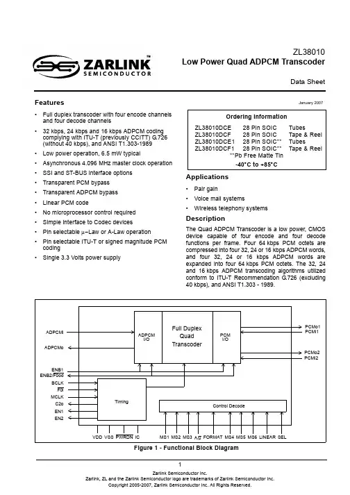
1Features•Full duplex transcoder with four encode channels and four decode channels•32kbps, 24kbps and 16kbps ADPCM coding complying with ITU-T (previously CCITT) G.726 (without 40kbps), and ANSI T1.303-1989•Low power operation, 6.5mW typical•Asynchronous 4.096MHz master clock operation •SSI and ST-BUS interface options •Transparent PCM bypass •Transparent ADPCM bypass •Linear PCM code•No microprocessor control required •Simple interface to Codec devices •Pin selectable µ−Law or A-Law operation •Pin selectable ITU-T or signed magnitude PCM coding•Single 3.3Volts power supplyApplications•Pair gain•Voice mail systems•Wireless telephony systemsDescriptionThe Quad ADPCM Transcoder is a low power, CMOS device capable of four encode and four decode functions per frame. Four 64kbps PCM octets are compressed into four 32, 24 or 16kbps ADPCM words,and four 32, 24 or 16 kbps ADPCM words are expanded into four 64kbps PCM octets. The 32, 24and 16kbps ADPCM transcoding algorithms utilized conform to ITU-T Recommendation G.726 (excluding 40kbps), and ANSI T1.303 - 1989.January 2007Ordering InformationZL38010DCE 28 Pin SOIC TubesZL38010DCF 28 Pin SOIC Tape & Reel ZL38010DCE128 Pin SOIC**TubesZL38010DCF128 Pin SOIC**Tape & Reel**Pb Free Matte Tin-40°C to +85°CZL38010Low Power Quad ADPCM TranscoderData SheetFigure 1 - Functional Block DiagramADPCM I/OPCM I/OControl DecodeVDD VSS PWRDN IC MS1MS2A/µFORMAT MS5MS4MS3MS6LINEAR SELTimingADPCMi ADPCMoENB1ENB2/F0odBCLK F0i MCLK C2o EN1EN2PCMo1PCMi1PCMo2PCMi2Full Duplex Quad TranscoderZL38010Data SheetSwitching, on-the-fly, between 32kbps and 24kbps ADPCM, is possible by controlling the appropriate mode select (MS1 - MS6) control pins. All optional functions of the device are pin selectable allowing a simple interface to industry standard codecs, digital phone devices and Layer 1 transceivers. Linear coded PCM is provided to facilitate external DSP functions.Change SummaryChanges from October 2005 Issue to January 2007 Issue.Figure 2 - Pin ConnectionsPin Description Page ItemChange1Ordering Information BoxAdded Pb Free part numbers.Pin #Name Description1EN1Enable Strobe 1 (Output). This 8 bit wide, active high strobe is active during the B1 PCM channel in ST-BUS mode. Becomes a single bit, high true pulse when LINEAR=1. In SSI mode this output is high impedance.2MCLKMaster Clock (input). This is a 4.096MHz (minimum) input clock utilized by thetranscoder function; it must be supplied in both ST-BUS and SSI modes of operation. In ST-BUS mode the C4 ST-BUS clock is applied to this pin. This synchronous clock is also used to control the data I/O flow on the PCM and ADPCM input/output pins according to ST-BUS requirements.In SSI mode this master clock input is derived from an external source and may beasynchronous with respect to the 8kHz frame. MCLK rates greater than 4.096MHz are acceptable in this mode since the data I/O rate is governed by BCLK.3F0i Frame Pulse (Input). Frame synchronization pulse input for ST-BUS operation. SSI operation is enabled by connecting this pin to V SS .4C2o2.048MHz Clock (Output). This ST-BUS mode bit clock output is the MCLK (C4) input divided by two, inverted, and synchronized to F0i. This output is high-impedance during SSI operation.12345678910111213141516171819202827262524232221MS1VDD MS3ICMS4FORMAT MS2PWRDN ADPCMi ADPCMo MS5MS6EN2PCMo1BCLK PCMi1LINEAR ENB2/F0odVSS C2o MCLK F0i PCMi2ENB1PCMo2EN1SEL A/µZL38010Data SheetPin #Name Description5BCLK Bit Clock (Input). 128kHz to 4096kHz bit clock input for both PCM and ADPCM ports;used in SSI mode only. The falling edge of this clock latches data into ADPCMi, PCMi1and PCMi2. The rising edge clocks data out on ADPCMo, PCMo1 and PCMo2. This inputmust be tied to V SS for ST-BUS operation.6PCMo1Serial PCM Stream 1 (Output). 128kbps to 4096kbps serial companded/linear PCM out-put stream. Data are clocked out by rising edge of BCLK in SSI mode. Clocked out byMCLK divided by two in ST-BUS mode. See Figure 14.7PCMi1Serial PCM Stream 1 (Input). 128kbps to 4096kbps serial companded/linear PCM input stream. Data are clocked in on falling edge of BCLK in SSI mode. Clocked in at the3/4 bit position of MCLK in ST-BUS mode. See Figure 14.8V SS Digital Ground. Nominally 0 volts9LINEAR Linear PCM Select (Input). When tied to V DD the PCM I/O ports (PCM1,PCM2) are 16-bit linear PCM. Linear PCM operates only at a bit rate of 2048kbps. Companded PCM isselected when this pin is tied to V SS. See Figure 5 & Figure 8.10ENB2/F0od PCM B-Channel Enable Strobe 2 (Input) / Delayed Frame Pulse (Output).SSI operation: ENB2 (Input). An 8-bit wide enable strobe input defining B2 channel(AD)PCM data. A valid 8-bit strobe must be present at this input for SSI operation. SeeFigure 4 & Figure 6.ST-BUS operation: F0od(Output). This pin is a delayed frame strobe output. When LIN-EAR=0, this becomes a delayed frame pulse output occurring 64 C4 clock cycles afterF0i and when LINEAR = 1 at 128 C4 clock cycles after F0i. See Figures 7, 8, 9 & 14.11ENB1PCM B-Channel Enable Strobe 1 (Input).SSI operation: An 8-bit wide enable strobe input defining B1 channel (AD)PCM data. Avalid 8-bit strobe must be present at this input for SSI operation.ST-BUS operation: When tied to V SS transparent bypass of the ST-BUS D- and C- chan-nels is enabled. When tied to V DD the ST-BUS D-channel and C-channel output timeslotsare forced to a high-impedance state.12PCMo2Serial PCM Stream 2 (Output). 128kbps to 4096kbps serial companded/linear PCM out-put stream. Clocked out by rising edge of BCLK in SSI mode. Clocked out by MCLK divid-ed by two in ST-BUS mode. See Figure 14.13PCMi2Serial PCM Stream 2 (Input). 128kbps to 4096kbps serial companded/linear PCM input stream. Data bits are clocked in on falling edge of BCLK in SSI mode. Clocked in at the3/4 bit position of MCLK in ST-BUS mode. See Figure 14.14SEL SELECT (Input).PCM bypass mode: When SEL=0 the PCM1 port is selected for PCM bypass operationand when SEL=1 the PCM2 port is selected for PCM bypass operation.See Figure 6 & Figure 9.16kbps transcoding mode:SSI Operation - in 16kbps transcoding mode, the ADPCM words are assigned to the I/Otimeslot defined by ENB2 when SEL=1 and by ENB1 when SEL=0. See Figure 4.ST-BUS operation- in 16kbps transcoding mode, the ADPCM words are assigned to theB2 timeslot when SEL=1 and to the B1 timeslot when SEL=0. See Figure 9.ZL38010Data SheetAll unused inputs should be connected to logic low or high unless otherwise stated. All outputs should be left open circuit when not used.All inputs have TTL compatible logic levels except for MCLK which has CMOS compatible logic levels and PWRDN which has Schmitt trigger compatible logic levels.All outputs are CMOS with CMOS logic levels (See DC Electrical Characteristics).15A/µA-Law/µ−Law Select (Input). This input pin selects µ−Law companding when set to logic 0, and A-Law companding when set to logic 1. This control is for all channels.This input is ignored in Linear mode during which it may be tied to V SS or V DD .16FORMATFORMAT Select (Input). Selects ITU-T PCM coding when high and Sign-Magnitude PCM coding when low. This control is for all channels.This input is ignored in Linear mode during which it may be tied to V SS or V DD .17PWRDN Power-down (Input). An active low reset forcing the device into a low power mode where all outputs are high-impedance and device operation is halted. 18IC Internal Connection (Input). Tie to V SS for normal operation.192021MS1MS2MS3Mode Selects 1, 2 and 3 (Inputs). Mode selects for all four encoders.MS3MS2MS1MODE 00032kbps ADPCM 00124kbps ADPCM 01016kbps ADPCM in EN1/ENB1 when SEL=0in EN2/ENB2 when SEL=1011ADPCM Bypass for 32kbps and 24kbps 100ADPCM Bypass for 16kbps 101PCM Bypass (64kbps) to PCM1 if SEL=0, PCM2 if SEL=1110Algorithm reset (ITU-T optional reset)111ADPCMo disable 22V DD Positive Power Supply. Nominally 3.3Volts +/-10%23ADPCMiSerial ADPCM Stream (Input). 128kbps to 4096kbps serial ADPCM word input stream. Data bits are clocked in on falling edge of BCLK in SSI mode and clocked in on the 3/4 bit edge of MCLK in ST-BUS mode.24ADPCMoSerial ADPCM Stream (Output). 128kbps to 4096kbps serial ADPCM word output stream. Data bits are clocked out by rising edge of BCLK in SSI mode and clocked out by MCLK divided by two in ST-BUS mode.252627MS4MS5MS6Mode Selects 4, 5 and 6 (Inputs). Mode selects for all four decoders.MS6MS5MS4MODE 00032kbps ADPCM 00124kbps ADPCM 01016kbps ADPCM in EN1/ENB1 when SEL=0in EN2/ENB2 when SEL=1011ADPCM Bypass for 32kbps and 24kbps 100ADPCM Bypass for 16kbps 101PCM Bypass (64kbps) to PCM1 if SEL=0, PCM2 if SEL=1110Algorithm reset (ITU-T optional reset)111PCMo1/2 disable 28EN2Enable Strobe 2 (Output). This 8 bit wide, active high strobe is active during the B2 PCM channel in ST-BUS mode. Forced to high impedance when LINEAR=1.Pin #Name DescriptionZL38010Data Sheet Functional DescriptionThe Quad-channel ADPCM Transcoder is a low power, CMOS device capable of four encode and four decode operations per frame. Four 64kbps channels (PCM octets) are compressed into four 32, 24 or 16kbps ADPCM channels (ADPCM words), and four 32, 24 or 16kbps ADPCM channels (ADPCM words) are expanded into four 64kbps PCM channels (PCM octets). The ADPCM transcoding algorithm utilized conforms to ITU-T recommendation G.726 (excluding 40kbps), and ANSI T1.303 - 1989. Switching on-the-fly between 32 and 24kbps transcoding is possible by toggling the appropriate mode select pins (supports T1 robbed-bit signalling). All functions supported by the device are pin selectable. The four encode functions comprise a common group controlled via Mode Select pins MS1, MS2 and MS3. Similarly, the four decode functions form a second group commonly controlled via Mode Select pins MS4, MS5 and MS6. All other pin controls are common to the entire transcoder.The device requires 6.5mWatts (MCLK= 4.096MHz) typically for four channel transcode operation. A minimum master clock frequency of 4.096MHz is required for the circuit to complete four encode channels and four decode channels per frame. For SSI operation a master clock frequency greater than 4.096MHz and asynchronous, relative to the 8kHz frame, is allowed.The PCM and ADPCM serial busses support both ST-BUS and Synchronous Serial Interface (SSI) operation. This allows serial data clock rates from 128kHz to 4096kHz, as well as compatibility with Zarlink’s standard Serial Telecom BUS (ST-BUS). For ST-BUS operation, on chip channel counters provide channel enable outputs as well as a 2048kHz bit clock output which may be used by down-stream devices utilizing the SSI bus interface.Linear coded PCM is also supported. In this mode the encoders compress, four 14-bit, two’s complement (S,S,S,12,...,1,0), uniform PCM channels into four 4, 3 or 2 bit ADPCM channels. Similarly, the decoder expands four 4, 3 or 2 bit ADPCM channels into four 16-bit, two’s complement (S,14,...,1,0), uniform PCM channels. The data rate for both ST-BUS and SSI operation in this mode is 2048 kbps.ZL38010Data Sheet Serial (AD)PCM Data I/OSerial data transfer to/from the Quad ADPCM transcoder is provided through one ADPCM and two PCM ports (ADPCMi, ADPCMo, PCMi1, PCMo1, PCMi2, PCMo2). Data is transferred through these ports according to either ST-BUS or SSI requirements. The device determines the mode of operation by monitoring the signal applied to the F0i pin. When a valid ST-BUS frame pulse (244nSec low going pulse) is applied to the F0i pin the transcoder will assume ST-BUS operation. If F0i is tied continuously to V SS the transcoder will assume SSI operation. Pin functionality in each of these modes is described in the following sub-sections.ST-BUS ModeDuring ST-BUS operation the C2o, EN1, EN2 and F0od outputs become active and all serial timing is derived from the MCLK (C4) and F0i inputs while the BCLK input is tied to V SS. (See Figures 7, 8 & 9.)Basic Rate “D” and “C” ChannelsIn ST-BUS mode, when ENB1 is brought low, transparent transport of the ST-BUS "Basic Rate D- and C-channels" is supported through the PCMi1 and PCMo1 pins. This allows a microprocessor controlled device, connected to the PCMi/o1 pins, to access the "D" and "C" channels of a transmission device connected to the ADPCMi/o pins. When ENB1 is brought high, the “D” and “C” channel outputs are tristated. Basic Rate “D” and “C” channels are not supported in LINEAR mode.(See Figure 7.)SSI ModeDuring SSI operation the BCLK, ENB1 and ENB2/F0od inputs become active. The C2o, EN1, and EN2 outputs are forced to a high-impedance state except during LINEAR operation during which the EN1 output remains active. (See Figures 4, 5 & 6.)The SSI port is a serial data interface, including data input and data output pins, a variable rate bit clock input and two input strobes providing enables for data transfers. There are three SSI I/O ports on the Quad ADPCM; the PCMi/o1 PCM port, the PCMi/o2 PCM port, and the ADPCMi/o port. The two PCM ports may transport 8-bit companded PCM or 16-bit linear PCM. The alignment of the channels is determined by the two input strobe signals ENB1 and ENB2/F0od. The bit clock (BCLK) and input strobes (ENB1 and ENB2/F0od) are common for all three of the serial I/O ports. BCLK can be any frequency between 128kHz and 4096kHz synchronized to the input strobes. BCLK may be discontinuous outside of the strobe boundaries except when LINEAR=1. In LINEAR mode, BCLK must be 2048kHz and continuous for 64 cycles after the ENB1 rising edge and for the duration of ENB2/F0od. Mode Select Operation (MS1, MS2, MS3, MS4, MS5, MS6)Mode Select pins MS1, MS2 and MS3 program different bit rate ADPCM coding, bypass, algorithmic reset and disable modes for all four encoder functions simultaneously. When 24kbps ADPCM mode is selected bit 4 is unused while in 16kbps ADPCM mode all ADPCM channels are packed contiguously into one 8-bit octet. Mode Select pins MS4, MS5 and MS6 operate in the same manner for the four decode functions. The mode selects must be set up according to the timing constraints illustrated in Figures 16 and 17.32 kbps ADPCM ModeIn 32kbps ADPCM mode, the 8-bit PCM octets of the B1, B2, B3 and B4 channels (PCMi1 and PCMi2) are compressed into four 4-bit ADPCM words on ADPCMo. Conversely, the 4-bit ADPCM words of the B1, B2, B3 and B4 channels from ADPCMi are expanded into four 8-bit PCM octets on PCMo1 and PCMo2. The 8-bit PCM octets (A-Law or µ-Law) are transferred most significant bit first starting with b7 and ending with b0. ADPCM words are transferred most significant bit first starting with I1 and ending with I4 (See Figures 4 & 7). Reference ITU-T G.726 for I-bit definitions.ZL38010Data Sheet24 kbps ADPCM ModeIn 24kbps mode PCM octets are transcoded into 3-bit words rather than the 4-bit words utilized in 32kbps ADPCM. This is useful in situations where lower bandwidth transmission is required. Dynamic operation of the mode select control pins will allow switching from 32kbps mode to 24kbps mode on a frame by frame basis. The 8 bit PCM octets (A-Law or µ-Law) are transferred most significant bit first starting with b7 and ending with b0. ADPCM words are transferred most significant bit first starting with I1 and ending with I3 (I4 becomes don’t care). (See Figures 4 & 7.)16 kbps ADPCM ModeWhen SEL is set to 0, the 8-bit PCM octets of the B1, B2, B3 and B4 channels (PCMi1 and PCMi2) are compressed into four 2-bit ADPCM words on ADPCMo during the ENB1 timeslot in SSI mode and during the B1 timeslot in ST-BUS mode. Similarly, the four 2-bit ADPCM words on ADPCMi are expanded into four 8-bit PCM octets (on PCMo1 and PCMo2) during the ENB1/B1 timeslot. (See Figures 4 & 7.)When SEL is set to 1, The same conversion takes place as described when SEL = 0 except that the ENB2/B2 timeslots are utilized.A-Law or µ-Law 8-bit PCM are received and transmitted most significant bit first starting with b7 and ending with b0. ADPCM data are most significant bit first starting with I1 and ending with I2.ADPCM BYPASS (32 and 24 kbps)In ADPCM bypass mode the B1 and B2 channel ADPCM words are bypassed (with a two-frame delay) to/from the ADPCM port and placed into the most significant nibbles of the PCM1/2 port octets. Note that the SEL pin performs no function for these two modes (See Figures 6 & 9). LINEAR, FORMAT and A/µ pins are ignored in bypass mode. In 32kbps ADPCM bypass mode, Bits 1 to 4 of the B1, B2, B3 and B4 channels from PCMi1 and PCMi2 are transparently passed, with a two frame delay, to the same channels on ADPCMo. In the same manner, the B1, B2, B3 and B4 channels from ADPCMi are transparently passed, with a two frame delay, to the same channels on PCMo1 and PCMo2 pins. Bits 5 to 8 are don’t care. This feature allows two voice terminals, which utilize ADPCM transcoding, to communicate through a system without incurring unnecessary transcode conversions. This arrangement allows byte-wide or nibble-wide transport through a switching matrix.24kbps ADPCM bypass mode is the same as 32 kbps mode bypass excepting that only bits 1 to 3 are bypassed and bits 4 to 8 are don’t care.ADPCM BYPASS (16 kbps)When SEL is set to 0, only bits 1 and 2 of the B1, B2, B3 and B4 PCM octets (on PCMi1 and PCMi2) are bypassed, with a two frame delay, to the same channels on ADPCMo during the ENB1 timeslot in SSI mode and during the B1 timeslot in ST-BUS mode. Similarly, the four 2-bit ADPCM words on ADPCMi are transparently bypassed, with a two frame delay, to PCMo1 and PCMo2 during the ENB1 or B1 timeslot. Bits 3-8 are don’t care. (See Figures 6 & 9.)When SEL is set to 1, the same bypass occurs as described when SEL = 0 except that the ENB2 or B2 timeslots are utilized.LINEAR, FORMAT and A/µ pins are ignored in bypass mode.ZL38010Data SheetPCM BYPASSWhen SEL is set to 0, the B1 and B2 PCM channels on PCMi1 are transparently passed, with a two-frame delay, to the same channels on the ADPCMo. Summarily, the two 8-bit words which are on ADPCMi are transparently passed, with a two-frame delay, to channels B1 and B2 of PCMo1 while PCMo2 is set to a high-impedance state.(See Figures 6 & 9.)When SEL is set to 1, the B3 and B4 channels on PCMi2 are transparently passed, with a two frame delay, to the same channels on ADPCMo. Similarly, the two 8-bit words which are on ADPCMi are transparently passed, with a two-frame delay, to channels B3 and B4 of PCMo2. In this case PCMo1 is always high-impedance if ENB1 = 0. If ENB1 = 1 during ST-BUS operation then the D and C channels are active on PCMo1.LINEAR, FORMAT and A/µ pins are ignored in bypass mode.Algorithm Reset ModeWhile an algorithmic reset is asserted the device will incrementally converge its internal variables to the 'Optional reset values' stated in G.726. Algorithmic reset requires that the master clock (MCLK) and frame pulse (ENB1/2 or F0i) remain active and that the reset condition be valid for at least four frames. Note that this is not a power down mode; see PWRDN for this function.ADPCMo & PCMo1/2 DisableWhen the encoders are programmed for ADPCMo disable (MS1 to MS3 set to 1) the ADPCMo output is set to a high impedance state and the internal encode function remains active. Therefore convergence is maintained. The decode processing function and data I/O remain active.When the decoders are programmed for PCMo1/2 disable (MS4 to MS6 set to 1) the PCMo1/2 outputs are high impedance during the B Channel timeslots and also, during ST-BUS operation, the D and C channel timeslots according to the state of ENB1. Therefore convergence is maintained. The encode processing function and data I/O remain active.Whenever any combination of the encoders or decoders are set to the disable mode the following outputs remain active. A) ST-BUS mode: ENB2/F0od, EN1, EN2 and C2o. Also the “D” and “C” channels from PCMo1 and ADPCMo remain active if ENB1 is set to 0. If ENB1 is brought high then PCMo1 and ADPCMo are fully tri-stated. B) SSI mode: When used in the 16-bit linear mode, only the EN1 output remains active. For complete chip power down see PWRDN.ZL38010Data Sheet Other Pin Controls16 Bit Linear PCMSetting the LINEAR pin to logic one causes the device to change to 16-bit linear (uniform) PCM transmission on the PCMi/o1 and PCMi/o2 ports. The data rate for both ST-BUS and SSI operation in this mode is 2048 kbps and all decode and encode functions are affected by this pin. In SSI mode, the input channel strobes ENB1 and ENB2/F0od remain active for 8 cycles of BCLK for an ADPCM transfer. The EN1 output is high for one BCLK period at the end of the frame (i.e., during the 256th BCLK period). In ST-BUS mode, the output strobes EN1 and ENB2/F0od are adjusted to accommodate the required PCM I/O streams. The EN1 output becomes a single bit high true pulse during the last clock period of the frame (i.e., the 256th bit period) while ENB2/F0od becomes a delayed, low true frame-pulse (F0od) output occurring during the 64th bit period after the EN1 rising edge.Linear PCM on PCMi1 and PCMi2, are received as 14-bit, two’s complement data with three bits of sign extension in the most significant positions (i.e., S,S,S,12,...1,0) for a total of 16 bits. The linear PCM data transmitted from PCMo1 and PCmo2 are 16-bit, two’s complement data with one sign bit in the most significant position (i.e., S,14,13,...1,0)32 and 24 kbps ADPCM modeIn 32kbps and 24kbps linear mode, the 16-bit uniform PCM dual-octets of the B1, B2, B3 and B4 channels (from PCMi1 and PCMi2) are compressed into four 4-bit words on ADPCMo. The four 4-bit ADPCM words of the B1, B2, B3 and B4 channels from ADPCMi are expanded into four 16-bit uniform PCM dual-octets on PCMo1 and PCMo2. 16-bit uniform PCM are received and transmitted most significant bit first starting with b15 and ending with b0. ADPCM data are transferred most significant bit first starting with I1 and ending with I4 for 32kbps and ending with I3 for 24kbps operation (i.e., I4 is don’t care).(See Figures 5 & 8.)16 kbps ADPCM modeWhen SEL is set to 0, the four, 2-bit ADPCM words are transmitted/received on ADPCMo/i during the ENB1 time-slot in SSI mode and during the B1 timeslot in ST-BUS mode. When SEL is set to 1, the four, 2-bit ADPCM words are transmitted/received on ADPCMo/i during the ENB2 timeslot in SSI mode and during the B2 timeslot in ST-BUS mode. (See Figures 5 & 8.)PCM Law Control (A/µ, FORMAT)The PCM companding/coding law invoked by the transcoder is controlled via the A/µ and FORMAT pins. ITU-T G.711 companding curves, µ-Law and A-Law, are selected by the A/µ pin (0=µ-Law; 1=A-Law). Per sample, digital code assignment can conform to ITU-T G.711 (when FORMAT=1) or to Sign-Magnitude coding (when FORMAT=0). Table 1 illustrates these choices.ZL38010Data SheetTable 1 - Companded PCMPower DownSetting the PWRDN pin low will asynchronously cause all internal operation to halt and the device to go to a power down condition where no internal clocks are running. Output pins C2o, EN1, EN2, PCMo1, PCMo2 and ADPCMo and I/O pin F0od/ENB2 are forced to a high-impedance state. Following the reset (i.e., PWRDN pin brought high)and assuming that clocks are applied to the MCLK and BCLK pins, the internal clocks will still not begin to operate until the first frame alignment is detected on the ENB1 pin for SSI mode or on the F0i pin for ST-BUS mode. The C2o clock and EN1, EN2 pins will not start operation until a valid frame pulse is applied to the F0i pin. If the F0i pin remains low for longer than 2 cycles of MCLK then the C2o pin will top toggling and will stay low. If the F0i pin is held high then the C2o pin will continue to operate. In ST-BUS mode the EN1 and EN2 pins will stop toggling if the frame pulse (F0i) is not applied every frame.Master Clock (MCLK)A minimum 4096kHz master clock is required for execution of the transcoding algorithm. The algorithm requires 512 cycles of MCLK during one frame for proper operation. For SSI operation this input, at the MCLK pin, may be asynchronous with the 8kHz frame provided that the lowest frequency and deviation due to clock jitter still meets the strobe period requirement of a minimum of 512 t C4P - 25%t C4P (see Figure 3). For example, a system producing large jitter values can be accommodated by running an over-speed MCLK that will ensure a minimum 512 MCLK cycles per frame is obtained. The minimum MCLK period is 61nSec, which translates to a maximum frequency of 16.384MHz. Extra MCLK cycles (>512/frame) are acceptable since the transcoder is aligned by the appropriate strobe signals each frame.Figure 3 - MCLK Minimum RequirementFORMAT01PCM CodeSign-Magnitude A/µ = 0 or 1ITU-T (G.711)(A/µ = 0)(A/µ = 1)+ Full Scale 1111 11111000 00001010 1010+ Zero 1000 00001111 11111101 0101- Zero 0000 00000111 11110101 0101- Full Scale0111 11110000 00000010 1010ENB1MCLK512 t C4P - 25%t C4P MinimumZL38010Data Sheet Bit Clock (BCLK)For SSI operation the bit rate, for both ADPCM and PCM ports, is determined by the clock input at BCLK. BCLK must be eight periods in duration and synchronous with the 8kHz frame inputs at ENB1 and ENB2. Data is sampled at PCMi1/2 and at ADPCMi concurrent with the falling edge of BCLK. Data is available at PCMo1/2 and ADPCMo concurrent with the rising edge of BCLK. BCLK may be any rate between 128kHz and 4096kHz. For ST-BUS operation BCLK is ignored (tie to V SS) and the bit rate is internally set to 2048kbps.Figure 4 - SSI 8-Bit Companded PCM Relative TimingZL38010Data SheetFigure 5 - SSI 16-Bit Linear PCM Relative TimingZL38010Data SheetFigure 6 - SSI PCM and ADPCM Bypass Relative TimingZL38010Data SheetFigure 7 - ST-BUS 8-Bit Companded PCM Relative TimingZL38010Data SheetFigure 8 - ST-BUS 16-Bit Linear PCM Relative TimingZL38010Data SheetFigure 9 - ST-BUS PCM and ADPCM Bypass Relative TimingZL38010Data Sheet Processing Delay Through the DeviceIn order to accommodate variable rate PCM and ADPCM interfaces, the serial input and output streams require a complete frame to load internal shift registers. Internal frame alignment of the encoding/decoding functions are taken from either of the F0i or ENB1 & ENB2 input strobes depending upon the device operating mode (i.e., ST-BUS or SSI). The encoding/decoding of all channels then takes one frame to complete before the output buffers are loaded. This results in a two frame transcoding delay. The two frame delay also applies to the D and C channels and to the PCM and ADPCM bypass functions.(See Figure 10.)Note: When changing the relative positions of the ENB1 and ENB2 strobes, precaution must be taken to ensure that two conditions are met. They are:1.There must be at least 512 master clock cycles between consecutive rising edges of ENB1. This condition alsoholds true for ENB2.2.The ENB1 strobe must alternate with the ENB2 strobe.Violation of these requirements may cause noise on the output channels.Figure 10 - Data ThroughputApplicationsFigure 11 depicts an ISDN line card utilizing a ’U’ interface transceiver and ZL38010 ADPCM transcoder. This central office application implements the network end of a Pair-Gain system. Figure 12 shows Zarlink devices used to construct the remote Pair-Gain loop terminator.。
U n i n t e r r u p t i b l eP o w e r S u p p l y用户手册U S E R′S M A N U A L10-40KVA三相输出Three-phase Outputpag. 2 / 29安全规范注意事项本手册包含安装与操作本产品的说明.。
请在安装前由经过专业训练的人员详细阅读本手册。
因为本手册包含基本的使用说明。
请妥善保存!安全规范■ 本产品安装时必须接地请确保地线牢固地索附在有右图标示的接地铜条上:■ 所有关于本产品内部的维修保养工作必须由经过专业训练的人员操作■ 在需要更换保险丝的情形时,请更换同样型式与规格的保险丝(请参阅”设置输出入配线”章节). ■ 在必须切断UPS 的输入市电时,请断开前面板内的所有开关,或者经由UPS 的控制面板选择”SYSTEM OFF”电瓶更换必须由专业人员执行.更换之后的废电瓶请交由专业的废电的处置,因为电池内 可能有对环境造成污染的物质!由于本产品不断的改良与研发,对于本手册内容有所修正时将不另行通知.欢迎您随时与我们联系以取得最新信息.电磁干扰要求本产品”不断电式电源供应器”(UPS),符合基本的电磁干扰要求:EMC 指令89/336e 92/31 a 93/68 ECC.使用说明警告:本产品属于A 等级的UPS.在居住的环境中,本产品可能会造成无线电干扰,此情况下,使用者可能必须采取适当的措施.例如:当电视或者收音机受到干扰时,可将本产品搬移到适当的距离以减少干扰情形.索引外观位置图 (5)储存 (5)安装环境 (6)前置作业 (6)安装环境 (6)安装位置 (6)设置输出入配线 (7)保护 (7)UPS内部 (7)UPS输入 (7)UPS 输出,短路与选择性 (7)差异 (8)配线与连接 (8)启动UPS前置作业 (8)市电与负载连接 (9)三相输出(输入:三相) (9)电瓶 (9)外接电瓶箱 (9)内接电瓶箱 (9)连接状况 (9)开机程序 (9)功能检查 (10)关机 (10)配置模式 (10)在线式(ON - LINE) (10)待机经济模式(STANDBY-ON operation) (10)操作模式 (11)电瓶操作模式(不属于稳压器配置模式) (11)旁路操作模式 (12)手动旁路维护模式 (12)维护 (13)UPS 部件 (13)输入 / 输出过滤器 (13)转换器 (13)pag. 3 / 29逆变器 (14)旁路 (14)SWMB (手动维护开关), SWIN, SWOUT (14)电瓶 (14)RS232 n.1 与 n. 2 介面 (14)讯号及指令面板 (14)EPO连接器 (15)规格 (16)系统 (16)转换器输入 (16)转换器输出 (17)电瓶 (17)输出逆变器 (17)旁路 (17)状态讯息显示 (18)概述 (18)警示灯号: LED (18)警告讯息 (19)控制面板 (20)基本选单 (20)Key menu 1, "?", HELP (20)Key menu 2 "测量" (20)Key menu 2, 2 : “输出测量” (21)Key menu 3 "KEY", 指令 (21)Key menu 3, 2: 电瓶测试 (21)Key menu 3, 5: 使用者自订 (22)Key menu 3, 5, 436215, 2: 工作模式和功率设定 (22)Key menu 3, 5, 436215,3:输出电压,旁路电压范围,旁路频率范围的设定 (22)Key menu 3, 5, 436215, 4:电池数量,电池浮充电压,电池容量设定 (22)Key menu 3, 5, 436215,5:电池定时自测试设定 (22)Key menu 3, 6: 逆变器关闭 / 切至旁路模式 (23)Key menu 3, 7: 系统完全关机设定 (23)Key menu 4:事件记录 (23)故障代码表 (25)附录 (27)尺寸 / 重量 (28)pag. 4 / 29pag. 5 / 29外观位置图1. 控制面板2. 上面板3. 前面板4. 滑轮5. 背面通风孔6. 散热孔7. 风扇网格 8. EPO 连接器9. REMOTE 连接器 10. RS232-2 通讯端口 11. RS232-1 通讯端口 12. 侧面板储存本产品的储存条件如下:温 度:0°- 40°C (32°- 104°F) 相对湿度:< 95%UPS 内含电瓶时:UPS 内部的电瓶会因为化学变化而自我放电.假如您并非要立即使用本产品,请注意外装箱上标示的再充电日期(此标示只有在UPS 内含电瓶时才会有),并在期限内再充电!再充电只要提供UPS输入电源并开机限内再充电,保持在”正常模式”下运作至少24小时安装环境三相输出额定容量 [kVA] 10 15 20 30 40 操作温度0 ± 40 °C最大相对湿度95 % (无冷凝)最大操作高度4000m尺寸 (长 x 宽 x 高) [mm] 505 x 720 x 1140 505 x825 x 1215 UPS 重量100 114 120 126 140在标称负载及电瓶充电时的能量损失.[kW / kcal /B.T.U.]0.760024001.0490036001.39120048002.1180071002.824009600允许通过的空气流速(室内装置)[立方公尺/小时] 370 557 742 1100 1400 最大漏电流 (mA) < 100 mA保护等级IP20配线箱体底部前置作业本产品出厂时附有:- 保证书- 使用手册·-Nr. 3输入电瓶保险丝,-Nr. 2 输入电瓶箱保险丝(假如内接电瓶存在时)安装环境· 避免灰尘量太大,或者空气内有其它粉尘类的物质.· 确认安装的地板可以承受UPS以及电瓶箱的重量(请参照”尺寸与重量”章节) · 请检查安装的地点有足够的空间,不会造成日后维修的困扰· UPS操作时的环境必须在0-40℃之间.本产品可以在0-40℃之间正常操作.建议最佳的UPS与电瓶操作温度是20-25℃之间.事实上,电瓶在20℃下的平均寿命是4年,而在30℃之下则寿命会减半.· 避免阳光直接照射及靠近热源.为了保持安装环境的温度如上所述,请装设适当的排热系统(请参照“规格”章节确认kcal/kW/B.T.U.参考值).你可以参考下列的做法:· 自然散热;· 强制散热:当外界温度(例如20℃比UPS的操作环境低(例如25℃);· 空调设备:当外界温度(例如30℃比UPS的操作环境高(例如25℃)安装位置对于安装位置请注意下列事项:• UPS 的前面板请留至少1公尺的空间以便日后维护方便.pag. 6 / 29• UPS后背板与墙壁间至少留下20公分的距离以保持散热风扇的排热效果;至少40公分以便维护.• 请勿放置任何物品于UPS的上方• 交流/直流输出入电源线可以从UPS的底部或者后方进入设置输出入配线保护UPS内部输出入的保护开关与保险丝如下所列(请查询方块图).更换保险丝时请依照下表所示的规格与型号.三相输出UPS开关及内部保护装置UPS型式开关保险丝[kVA] UPS输入UPS 输出 / 维护整流器输入保险丝电瓶保险丝旁路保险丝输入电流.输出电流.[A]SWIN SWOUT/SWMB FBAT FBY 最大值额定值10 32A(4P) 32A(4P) 25AgR(10x38)25A gR(10x38)25A gG(10x38) 18 14 15 32A(4P) 32A(4P) 32AgR(10x38)32A gR(10x38)32A gG(10x38) 26 2620 32A(4P) 32A(4P) 32AgR(10x38)32A gR(10x38)50A gR(14x51)32A gG(10x38) 35 3530 63A(4P) 63A(4P) 50AgR(14x51)50A gR(14x51)50A gG(14x51) 52 4440 80A(4P) 80A(4P) 63AgR(14x51)80A gR(14x51)63A gG(14x51) 70 61 UPS 输入.当安装输入保护装置时,请考量下列两种模式的最大可能电流:• 在"正常操作"模式, 由输入电源至整流器, “最大输入电流” 如上表所列.断路器在整流器输入位置, 如上表中的"SWIN".• 在"旁路操作"模式, 旁路的最大电流值由断路器"SWBY”保护.UPS 输出, 短路与选择性额定的输出入电流如上表所示.短路当 UPS的负载发生异常状况时,也就是短路,UPS将会经由限制供应的输出电流值做自我保护 (短路电流).视短路发生时的操作状况.可以分成两方面:• UPS 在正常模式下:UPS将马上切换到旁路模式,在保险丝动作前,电流值如同“旁路规格” 表所示.• UPS 在电瓶供电模式下:UPS 提供两倍的额定输出电流(0.1秒)选择性在正常操作模式下,选择性参照第二行。
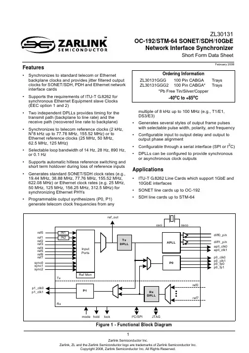
1Features•Synchronizes to standard telecom or Ethernet backplane clocks and provides jitter filtered output clocks for SONET/SDH, PDH and Ethernet network interface cards•Supports the requirements of ITU-T G.8262 for synchronous Ethernet Equipment slave Clocks (EEC option 1 and 2)•Two independent DPLLs provides timing for the transmit path (backplane to line rate) and the receive path (recovered line rate to backplane) •Synchronizes to telecom reference clocks (2kHz, N*8kHz up to 77.76MHz, 155.52MHz) or to Ethernet reference clocks (25MHz, 50MHz, 62.5MHz, 125MHz)•Selectable loop bandwidth of 14Hz, 28Hz, 890Hz, or 0.1Hz•Supports automatic hitless reference switching and short term holdover during loss of reference inputs •Generates standard SONET/SDH clock rates (e.g., 19.44MHz, 38.88MHz, 77.76MHz, 155.52MHz, 622.08MHz) or Ethernet clock rates (e.g. 25MHz, 50MHz, 125MHz, 156.25MHz, 312.5MHz) for synchronizing Ethernet PHYs•Programmable output synthesizers (P0, P1) generate telecom clock frequencies from anymultiple of 8kHz up to 100MHz (e.g., T1/E1, DS3/E3)•Generates several styles of output frame pulses with selectable pulse width, polarity, and frequency •Configurable input to output delay and output to output phase alignment•Configurable through a serial interface (SPI or I 2C)•DPLLs can be configured to provide synchronous or asynchronous clock outputsApplications•ITU-T G.8262 Line Cards which support 1GbE and 10GbE interfaces•SONET line cards up to OC-192•SDH line cards up to STM-64February 2008Figure 1 - Functional Block DiagramZL30131OC-192/STM-64 SONET/SDH/10GbENetwork Interface SynchronizerShort Form Data SheetOrdering InformationZL30131GGG 100 Pin CABGA TraysZL30131GGG2 100 Pin CABGA*Trays*Pb Free Tin/Silver/Copper-40o C to +85o CZL30131Short Form Data Sheet Pin DescriptionPin # Name I/OType DescriptionInput ReferenceC1 B2 A3 C3 B3 B4 C4 A4ref0ref1ref2ref3ref4ref5ref6ref7I u Input References 7:0 (LVCMOS, Schmitt Trigger). These input references areavailable to both the Tx DPLL and the Rx DPLL for synchronizing output clocks.All eight input references can lock to any multiple of 8kHz up to 77.76MHzincluding 25MHz and 50MHz. Input ref0 and ref1 have additional configurablepre-dividers allowing input frequencies of 62.5MHz, 125MHz, and 155.52MHz.These pins are internally pulled up to V dd.B1 A1 A2sync0sync1sync2I u Frame Pulse Synchronization References 2:0 (LVCMOS, Schmitt Trigger).These are optional frame pulse synchronization inputs associated with inputreferences 0, 1 and 2. These inputs accept frame pulses in a clock format (50%duty cycle) or a basic frame pulse format with minimum pulse width of 5 ns.These pins are internally pulled up to V dd.Output Clocks and Frame PulsesA9 B10diff0_pdiff0_nO Differential Output Clock 0 (LVPECL). When in SONET/SDH mode, this output can be configured to provide any one of the available SONET/SDH clocks(6.48MHz, 19.44MHz, 38.88MHz, 51.84MHz, 77.76MHz, 155.52MHz,311.04MHz, 622.08MHz). When in Ethernet mode, this output can beconfigured to provide any of the Ethernet clocks (25MHz, 50MHz, 62.5MHz,125MHz, 156.25MHz, 312.5MHz). See “Output Clocks and Frame Pulses”section on page22 more detail on clock frequency settings.A10 B9diff1_pdiff1_nO Differential Output Clock 1 (LVPECL). When in SONET/SDH mode, this output can be configured to provide any one of the available SONET/SDH clocks(6.48MHz, 19.44MHz, 38.88MHz, 51.84MHz, 77.76MHz, 155.52MHz,311.04MHz, 622.08MHz). When in Ethernet mode, this output can beconfigured to provide any of the Ethernet clocks (25MHz, 50MHz, 62.5MHz,125MHz, 156.25MHz, 312.5MHz). See “Output Clocks and Frame Pulses”section on page22 more detail on clock frequency settings.D10apll_clk0O APLL Output Clock 0 (LVCMOS). This output can be configured to provide anyone of the SONET/SDH clock outputs up to 77.76MHz or any of the Ethernetclock rates up to 125MHz. The default frequency for this output is 77.76MHz.G10apll_clk1O APLL Output Clock 1 (LVCMOS). This output can be configured to provide anyone of the SONET/SDH clock outputs up to 77.76MHz or any of the Ethernetclock rates up to 125MHz. The default frequency for this output is 19.44MHz.K9p0_clk0O Programmable Synthesizer 0 - Output Clock 0 (LVCMOS). This output can beconfigured to provide any frequency with a multiple of 8kHz up to 100MHz inaddition to 2kHz. The default frequency for this output is 2.048MHz.K7p0_clk1O Programmable Synthesizer 0 - Output Clock 1 (LVCMOS). This is aprogrammable clock output configurable as a multiple or division of the p0_clk0frequency within the range of 2 kHz to 100 MHz. The default frequency for thisoutput is 8.192MHz.K8p0_fp0O Programmable Synthesizer 0 - Output Frame Pulse 0 (LVCMOS). This outputcan be configured to provide virtually any style of output frame pulse associatedwith the p0 clocks. The default frequency for this frame pulse output is 8kHz.ZL30131Short Form Data SheetJ7p0_fp1OProgrammable Synthesizer 0 - Output Frame Pulse 1 (LVCMOS). This output can be configured to provide virtually any style of output frame pulse associated with the p0 clocks. The default frequency for this frame pulse output is 8kHz J10p1_clk0OProgrammable Synthesizer 1 - Output Clock 0 (LVCMOS). This output can be configured to provide any frequency with a multiple of 8kHz up to 100MHz in addition to 2kHz. The default frequency for this output is 1.544MHz (DS1).K10p1_clk1OProgrammable Synthesizer1 - Output Clock 1 (LVCMOS). This is a programmable clock output configurable as a multiple or division of the p1_clk0frequency within the range of 2kHz to 100MHz. The default frequency for this output is 3.088MHz (2x DS1).E1ref_out ORx DPLL Selected Output Reference (LVCMOS). This is a buffered copy of the output of the reference selector for the Rx DPLL. Switching between input reference clocks at this output is not hitless.Control H5rst_bIReset (LVCMOS, Schmitt Trigger). A logic low at this input resets the device. To ensure proper operation, the device must be reset after power-up. Reset should be asserted for a minimum of 300ns.J5hs_enI uTx DPLL Hitless Switching Enable (LVCMOS, Schmitt Trigger). A logic high at this input enables hitless reference switching. A logic low disables hitless reference switching and re-aligns the Tx DPLL’s output phase to the phase of the selected reference input. This feature can also be controlled through software registers. This pin is internally pulled up to Vdd.C2D2mode_0mode_1I uTx DPLL Mode Select 1:0 (LVCMOS, Schmitt Trigger). During reset, the levels on these pins determine the default mode of operation for the Tx DPLL (Automatic, Normal, Holdover or Freerun). After reset, the mode of operation can be controlled directly with these pins, or by accessing the tx_dpll_modesel register (0x1F) through the serial interface. This pin is internally pulled up to Vdd.K1diff0_enI uDifferential Output 0 Enable (LVCMOS, Schmitt Trigger). When set high, the differential LVPECL output 0 driver is enabled. When set low, the differential driver is tristated reducing power consumption. This pin is internally pulled up to Vdd.D3diff1_enI uDifferential Output 1 Enable (LVCMOS, Schmitt Trigger). When set high, the differential LVPECL output 1 driver is enabled. When set low, the differential driver is tristated reducing power consumption.This pin is internally pulled up to Vdd.Status H1lockOLock Indicator (LVCMOS). This is the lock indicator pin for the Tx DPLL. This output goes high when the Tx DPLL’s output is frequency and phase locked to the input reference.J1hold OHoldover Indicator (LVCMOS). This pin goes high when the Tx DPLL enters the holdover mode.Pin # Name I/O Type DescriptionZL30131Short Form Data SheetSerial Interface E2sck_sclI/BClock for Serial Interface (LVCMOS). Serial interface clock. When i2c_en = 0,this pin acts as the sck pin for the serial interface. When i2c_en = 1, this pin acts as the scl pin (bidirectional) for the I 2C interface.F1si_sda I/BSerial Interface Input (LVCMOS). Serial interface data pin. When i2c_en = 0,this pin acts as the si pin for the serial interface. When i2c_en = 1, this pin acts as the sda pin (bidirectional) for the I 2C interface.G1so OSerial Interface Output (LVCMOS). Serial interface data output. When i2c_en =0, this pin acts as the so pin for the serial interface. When i2c_en = 1, this pin is unused and should be left unconnected.E3cs_b_asel0I uChip Select for SPI/Address Select 0 for I 2C (LVCMOS). When i2c_en = 0, this pin acts as the chip select pin (active low) for the serial interface. When i2c_en =1, this pin acts as the asel0 pin for the I 2C interface.F3asel1I uAddress Select 1 for I 2C (LVCMOS). When i2c_en = 1, this pin acts as the asel1 pin for the I 2C interface. Internally pulled up to Vdd. Leave open when not in use.F2asel2I uAddress Select 2 for I 2C (LVCMOS). When i2c_en = 1, this pin acts as the asel2 pin for the I 2C interface. Internally pulled up to Vdd. Leave open when not in use.G2int_b OInterrupt Pin (LVCMOS). Indicates a change of device status prompting the processor to read the enabled interrupt service registers (ISR). This pin is an open drain, active low and requires an external pulled-up to Vdd.J2i2c_enI uI 2C Interface Enable (LVCMOS). If set high, the I 2C interface is enabled, if set low, the SPI interface is enabled. Internally pull-up to Vdd.APLL Loop Filter A6apll_filter A External Analog PLL Loop Filter terminal.B6filter_ref0A Analog PLL External Loop Filter Reference.C6filter_ref1AAnalog PLL External Loop Filter Reference.JTAG and Test J4tdoOTest Serial Data Out (Output). JTAG serial data is output on this pin on the falling edge of tck. This pin is held in high impedance state when JTAG scan is not enabled.K2tdiI uTest Serial Data In (Input). JTAG serial test instructions and data are shifted in on this pin. This pin is internally pulled up to Vdd. If this pin is not used then it should be left unconnected.H4trst_bI uTest Reset (LVCMOS). Asynchronously initializes the JTAG TAP controller by putting it in the Test-Logic-Reset state. This pin should be pulsed low on power-up to ensure that the device is in the normal functional state. This pin is internally pulled up to Vdd. If this pin is not used then it should be connected to GND.K3tck ITest Clock (LVCMOS): Provides the clock to the JTAG test logic. If this pin is not used then it should be pulled down to GND.Pin #NameI/O TypeDescriptionZL30131Short Form Data Sheet J3tms I u Test Mode Select (LVCMOS). JTAG signal that controls the state transitions ofthe TAP controller. This pin is internally pulled up to V DD. If this pin is not usedthen it should be left unconnected.Master ClockK4osci I Oscillator Master Clock Input (LVCMOS). This input accepts a 20MHzreference from a clock oscillator (TCXO, OCXO). The stability and accuracy ofthe clock at this input determines the free-run accuracy and the long termholdover stability of the output clocks.K5osco O Oscillator Master Clock Output (LVCMOS). This pin must be left unconnectedwhen the osci pin is connected to a clock oscillator.MiscellaneousJ6IC Internal Connection. Connect to ground.C5B5K6H10IC Internal Connection. Leave unconnected.H7G3E10F10D1NC No Connection. Leave Unconnected.Power and GroundD9 E4 G8 G9 J8 J9 H6 H8V DD PPPPPPPPPositive Supply Voltage. +3.3V DC nominal.E8 F4V CORE PPPositive Supply Voltage. +1.8V DC nominal.A5 A8 C10AV DD PPPPositive Analog Supply Voltage. +3.3V DC nominal.B7 B8 H2AV CORE PPPPositive Analog Supply Voltage. +1.8V DC nominal.Pin # Name I/OType DescriptionZL30131Short Form Data SheetI - InputI d -Input, Internally pulled down I u -Input, Internally pulled up O -Output A -Analog P -Power G -GroundD4D5D6D7E5E6E7F5F6F7G4G5G6G7E9F8F9H9V SSG G G G G G G G G G G G G G G G G G Ground. 0 Volts.A7C7C8C9D8H3AV SSG G G G G GAnalog Ground. 0 Volts.Pin # Name I/O Type DescriptionZL30131Short Form Data Sheet1.0 Pin DiagramBCDEFGHJK234567891011 - A1 corner is identified with a dot.Async1TOP VIEWsync2ref2ref7AV DDapll_filterAV SSAV DDdiff0_pdiff1_psync0ref1ref4ref5ICfilter_ref0AV COREAV COREdiff1_ndiff0_nref0mode_0ref3ref6ICfilter_ref1AV SSAV SSAV SSAV DDNCmode_1diff1_enV SSV SSV SSV SSAV SSV DDapll_clk0ref_outsck/ cs_b/VDDV SSV SSV SSV COREV SSNCsi/asel2asel1V COREV SSV SSV SSV SSV SSNCsoint_bNCV SSV SSV SSV SSV DDV DDapll_clk1lockAV COREAV SStrst_brst_bV DDNCV DDV SSICholdi2c_entmstdohs_enICp0_fp1V DDV DDp1_clk0diff0_entditckoscioscoICp0_clk1p0_fp0p0_clk0p1_clk11scl sdhasel0ZL30131Short Form Data Sheet 2.0 Functional DescriptionThe ZL30131 OC-192/STM-64 PDH/SONET/SDH/10GbE Network Interface Synchronizer is a highly integrated device that provides timing for both PDH/SONET/SDH and Ethernet network interface cards. A functional block diagram is shown in Figure 1.This device is ideally suited for designs that require both a transmit timing path (backplane to PHY) and a receive timing path (PHY to backplane). Each path is controlled with separate DPLLs (Tx DPLL, Rx DPLL) which are both independently configurable through the serial interface (SPI or I2C). A typical application of the ZL30131 is shown in Figure 2. In this application, the ZL30131 translates the 19.44MHz clock from the telecom rate backplane (system timing bus), translates the frequency to 622.08MHz or 156.25MHz for the PHY Tx clock, and filters the jitter to ensure compliance with the related standards. A programmable synthesizer (P0) provides synchronous PDH clocks with multiples of 8kHz for generating PDH interface clocks. On the receive path, the Rx DPLL and the P1 synthesizer translate the line recovered clock (8kHz or 25MHz) from the PHY to the 19.44MHz telecom backplane (line recovered timing) for the central timing cards. The ZL30131 allows easy integration of Ethernet line rates with today’s telecom backplanes.Figure 2 - Typical Application of the ZL30131Information relating to products and services furnished herein by Zarlink Semiconductor Inc. or its subsidiaries (collectively “Zarlink”) is believed to be reliable.However, Zarlink assumes no liability for errors that may appear in this publication, or for liability otherwise arising from the application or use of any such information, product or service or for any infringement of patents or other intellectual property rights owned by third parties which may result from such application or use. Neither the supply of such information or purchase of product or service conveys any license, either express or implied, under patents or other intellectual property rights owned by Zarlink or licensed from third parties by Zarlink, whatsoever. Purchasers of products are also hereby notified that the use of product in certain ways or in combination with Zarlink, or non-Zarlink furnished goods or services may infringe patents or other intellectual property rights owned by Zarlink.This publication is issued to provide information only and (unless agreed by Zarlink in writing) may not be used, applied or reproduced for any purpose nor form part of any order or contract nor to be regarded as a representation relating to the products or services concerned. The products, their specifications, services and other information appearing in this publication are subject to change by Zarlink without notice. No warranty or guarantee express or implied is made regarding the capability, performance or suitability of any product or service. Information concerning possible methods of use is provided as a guide only and does not constitute any guarantee that such methods of use will be satisfactory in a specific piece of equipment. It is the user’s responsibility to fully determine the performance and suitability of any equipment using such information and to ensure that any publication or data used is up to date and has not been superseded. Manufacturing does not necessarily include testing of all functions or parameters. These products are not suitable for use in any medical products whose failure to perform may result in significant injury or death to the user. All products and materials are sold and services provided subject to Zarlink’s conditions of sale which are available on request.Purchase of Zarlink’s I 2C components conveys a licence under the Philips I 2C Patent rights to use these components in and I 2C System, provided that the system conforms to the I 2C Standard Specification as defined by Philips.Zarlink, ZL and the Zarlink Semiconductor logo are trademarks of Zarlink Semiconductor Inc.Copyright Zarlink Semiconductor Inc. All Rights Reserved.TECHNICAL DOCUMENTATION - NOT FOR RESALEFor more information about all Zarlink productsvisit our Web Site at。
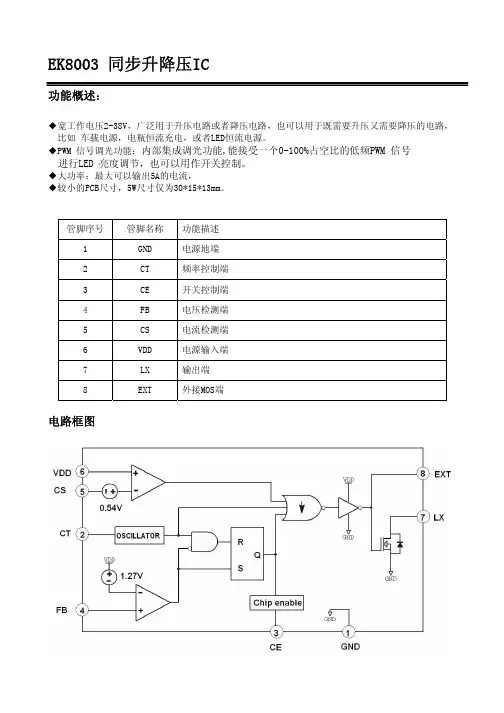
EK8003 同步升降压IC功能概述:◆宽工作电压2-38V,广泛用于升压电路或者降压电路,也可以用于既需要升压又需要降压的电路, 比如 车载电源,电瓶恒流充电,或者LED恒流电源。
◆PWM 信号调光功能:内部集成调光功能,能接受一个0-100%占空比的低频PWM 信号进行LED 亮度调节,也可以用作开关控制。
◆大功率:最大可以输出5A的电流,◆较小的PCB尺寸,5W尺寸仅为30*15*13mm。
管脚序号 管脚名称 功能描述1 GND 电源地端2 CT 频率控制端3 CE 开关控制端4 FB 电压检测端5 CS 电流检测端6 VDD 电源输入端7 LX 输出端8 EXT 外接MOS端电路框图应用1.应用2.应用指南:1) 电压计算:V OUT=1.27x(1+R3/R1),电流计算:I OUT=0.54V/R32) PWM/EN 端(3 脚)可以输入一个100~1000Hz 的低频PWN 信号进行亮度调节,如果不需调光则此端接地。
电感计算:一般来讲在输出相同电压的情况下,输出电流越小电感量要相对加大,而在输出相同电流的情况下,输出电压越高电感量要相对加大。
电感量调整不适当会发生电感响的问题。
4) 输出电容C3的计算:输出电流小的情况下可以用220uF,输出电流为300mA以上建议用470uF或者更大容量的电容,电容量小也会发生电感响的问题。
极限参数:参数 符号 测试条件件 最小值典型值 最大值 单位 工作频率 Fosc Ta=25℃ 20 300 KHz 工作电压 Vcc 2 38 V IC 各端极限电压 Vmax 38 V CE脚ON V CE0 1 V CE脚OFF V CE 2 38 V 电压检测端 V FB Ta=25℃ 1.24 1.27 1.3 V 调光频率 F PWM 100 500 1000 Hz LX最大输出电流 Iout 700 mA 电流检测端 SEN Vcc=3-36V Vpin3>V EN 0.510.54 0.57 mV 工作温度范围 Topr - 40 85 ℃储存环境温度 Tstg - 65 150 ℃焊接温度250±5℃ 260℃,10s抗静电强度 2000V 封装尺寸。
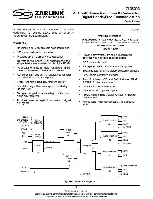
1A full Design Manual is available to qualified customers. To register, please send an email to VoiceProcessing@.Features•Handles up to -6dB acoustic echo return loss •127ms acoustic echo canceller•Provides up to 12dB of Noise Reduction •Operate in two modes, Dual Analog mode and single Analog mode (other port is digital PCM)•PCM Data Formats in single Port mode- 16-bit Linear, companded ITU-T A-law or U-law •Advanced NLP design - full duplex speech with no switched loss on audio paths•Tracks changing echo environment quickly •Adaptation algorithm converges even during Double-Talk•Designed for performance in high background noise environments•Provides protection against narrow-band signal divergence•Howling prevention eliminates uncontrolled oscillation in high loop gain conditions •AGC on speaker path•Transparent data transfer and mute options •Boot loadable for future factory software upgrades •Serial micro-controller interface•Two 16 bit linear ACD and DAC that meet ITU-T G.711/712 recommendations •Four Audio TX/RX Interfaces •Differential Microphone Inputs•Programmable Bias Voltage Output for Electret microphones•Microphone Presence Detection, Microphone MuteMay 2006Ordering InformationZL38003GMG 81 Ball CBGA Trays, Bake & Drypack ZL38003GMG281 Ball CBGA**Trays, Bake & Drypack**Pb Free Tin/Silver/Copper-40°C to +85°CZL38003AEC with Noise Reduction & Codecs forDigital Hands-Free CommunicationData SheetFigure 1 - Block DiagramSerial Microport InterfaceG.712Codec #1CrosspointG.712Codec #0AECAudio Interface#3Audio Interface#2Audio Interface#1Audio Interface#0AUXTONEEARMIC BIAS MICDETRESETBEARMIC BIAS MICDETEAR MICEAR/SPEAKER MIC BIASMCLK FPi C4i RinSoutSin/RinRout/SoutSCLK CS_CODEC CS_AECDATA1DATA2PCM Timing•Multiple Gain pad settings •Adjustable gain pads from -24dB to +21dB at Xin, Sin and Sout to compensate for different system requirements•Programmable Microphone Gain (0dB to +46.5dB in 1.5dB Steps)•Side tone Mute, Programmable Side tone Gain (-39dB to +6dB in 3dB Steps)•User gain control provided for speaker path (-24dB to +21dB in 3dB steps)•Programmable Earpiece Gain (-28dB to +2dB in 2dB Steps)•RX Channel Mute, Programmable RX Volume control (-21dB to 0dB in 3dB Steps)•Differential Earpiece Driver Outputs (66mW rms into 32 Ohms, 150mW rms into 16 Ohms)•Cross-Point Connects PCM Channels to any of the Four Audio TX/RX InterfacesApplications•Hands-free car kits•Full duplex speaker-phone for digital telephone •Echo cancellation for video conferences •Intercom Systems •Security Systems1.0 Functional DescriptionThe ZL38003 is an Acoustic Echo Canceller (AEC) with dual codec as shown in Figure 2. The ZL38003 provides 127ms of acoustic echo cancellation, which makes it ideal for hand free car kits, and speaker phones designs.Each of the codecs in the dual codec can be connected to 1 of 4 four analog ports through a cross point switch.Also, the network side can be routed to a digital PCM interface that input/outputs either linear 2's complement or A-/mu law commanded PCM data.MT93L16ZL38001ZL38002ZL38003Description AEC for analog hands-free communicationAEC for analog hands-free communication AEC with noise reduction for digital hands-free communicationAEC with noise reduction & codecs for digital hands-free communicationApplication Analog Desktop phone Analog Intercom Analog Desktop phone Analog Intercom Hands-free Car KitsDigital Desktop Phone Home Security Intercom & Pedestals Hands-free Car Kits Digital Desktop Phone Home SecurityIntercom & Pedestals Features AEC 1 channel 1 channel 1 channel 1 channel LEC 1 channel 1 channel Custom LoadCustom LoadGains User GainUser Gain/18dB Gain on SoutUser Gain + System tuning gainsUser Gain + System tuning gainsNoiseReduction N N Y Y Integrated CodecsNNNdual channelTable 1 - Acoustic Echo Cancellation Family2.0 Acoustic Echo Canceller (AEC) DescriptionThe AEC section is comprised of an acoustic echo canceller, noise reduction and the operational control functions for operation. The AEC guarantees clear signal transmission in both transmit and receive audio path directions ensuring reliable voice communication even when low level signals are provided. The AEC does not use variable attenuators during double-talk or single-talk periods of speech, as do many other acoustic echo cancellers for speakerphones. Instead, the AEC provides high performance full-duplex operation similar to network echo cancellers. This results in users experiencing clear speech and uninterrupted background signals during the conversation and prevents subjective sound quality problems associated with “noise gating” or “noise contrasting”.The AEC uses an advanced adaptive filter algorithm that is double-talk stable, allowing convergence even while both parties are talking. This algorithm continually tracks changes in the echo path, regardless of double-talk, as long as a reference signal is available for the echo canceller.The echo tail cancellation capability of the acoustic echo canceller has been sized appropriately (127ms) to cancel echo in an average sized office or large size car with a reverberation time of less than 127ms.Figure 2 - AEC Block DiagramRoutSinMicro InterfaceProgram RAM Program ROMHowling ControllerNBSDLinear/µ/A-LawR 1R 1S 1S 2L inear/µ/A-LawHP Filter Linearµ/A-Law/Adaptive FilterHP FilterSoutRinAGCUser Gain +--24 -> +21dBADV NLPLinearµ/A-Law/+UNIT CONTROL DetectorTalk Double NBSDLimiterLimiterA C O U S T I C E C H O P A T HGain PadGain PadGain Pad Noise Reduction2.1 In addition to the echo cancellers, the following functions are supported:•12dB of noise reduction•User gain control provided for speaker path (-24dB to +21dB in 3dB steps)•Gain pads at the Sin and Sout ports plus one at the input of adaptive filter (XRAM)•Control of adaptive filter convergence speed during periods of double-talk, far end single-talk and near-end echo path changes•Control of Non-Linear Processor thresholds for suppression of residual non-linear echo•Howling detector to identify when instability is starting to occur and to take action to prevent oscillation •Narrow-Band Detector for preventing adaptive filter divergence caused by narrow-band signals •Programmable high pass filters at Rin and Sin for removal of DC components in PCM channels•Limiters that introduce controlled saturation levels•Serial controller interface compatible with Motorola, National and Intel micro controllers•PCM encoder/decoder compatible with m/A-Law ITU-T G.711, m/A-Law Sign-Mag or linear 2’s complement coding•Automatic gain control on the receive speaker path•Idle channel noise suppression3.0 Dual Codec DescriptionThe CODEC Dual Codec provides complete audio to PCM interfaces including filtering and optional data companding as required by the ITU-T G.711 & G.712 recommendations. Programmable gain allows adjustment for a wide range of transducer sensitivities - two microphone amplifiers and four ear piece amplifiers are provided to allow connection to a handset, headset, auxiliary channel and microphone/speaker. A cross-point circuit allows either codec to be connected to any of the four audio interfaces. Programmable voltage sources are available for electret biasing on the Microphone channels.PCM voice data is passed via a serial interface which operates in ST-BUS or GCI mode. ST-BUS mode allows the Codecs to be allocated to any of the 32 available channels. Control and programming of the Codecs is carried out over a flexible serial micro-controller interface.Figure 3 - Block DiagramInformation relating to products and services furnished herein by Zarlink Semiconductor Inc. or its subsidiaries (collectively “Zarlink”) is believed to be reliable.However, Zarlink assumes no liability for errors that may appear in this publication, or for liability otherwise arising from the application or use of any such information, product or service or for any infringement of patents or other intellectual property rights owned by third parties which may result from such application or use. Neither the supply of such information or purchase of product or service conveys any license, either express or implied, under patents or other intellectual property rights owned by Zarlink or licensed from third parties by Zarlink, whatsoever. Purchasers of products are also hereby notified that the use of product in certain ways or in combination with Zarlink, or non-Zarlink furnished goods or services may infringe patents or other intellectual property rights owned by Zarlink.This publication is issued to provide information only and (unless agreed by Zarlink in writing) may not be used, applied or reproduced for any purpose nor form part of any order or contract nor to be regarded as a representation relating to the products or services concerned. The products, their specifications, services and other information appearing in this publication are subject to change by Zarlink without notice. No warranty or guarantee express or implied is made regarding the capability, performance or suitability of any product or service. Information concerning possible methods of use is provided as a guide only and does not constitute any guarantee that such methods of use will be satisfactory in a specific piece of equipment. It is the user’s responsibility to fully determine the performance and suitability of any equipment using such information and to ensure that any publication or data used is up to date and has not been superseded. Manufacturing does not necessarily include testing of all functions or parameters. These products are not suitable for use in any medical products whose failure to perform may result in significant injury or death to the user. All products and materials are sold and services provided subject to Zarlink’s conditions of sale which are available on request.Purchase of Zarlink’s I 2C components conveys a licence under the Philips I 2C Patent rights to use these components in and I 2C System, provided that the system conforms to the I 2C Standard Specification as defined by Philips.Zarlink, ZL and the Zarlink Semiconductor logo are trademarks of Zarlink Semiconductor Inc.Copyright Zarlink Semiconductor Inc. All Rights Reserved.TECHNICAL DOCUMENTATION - NOT FOR RESALEFor more information about all Zarlink productsvisit our Web Site at。
1Features•Meets jitter requirements of Telcordia GR-253-CORE for OC-192, OC-48, OC-12, and OC-3 rates•Meets jitter requirements of ITU-T G.813 for STM-64, STM-16, STM-4 and STM-1 rates•Provides four LVPECL differential output clocks at 622.08 MHz•Provides a CML differential clock at 155.52 MHz •Provides a single-ended CMOS clock at 19.44 MHz•Lock Indicator•Provides enable/disable control of output clocks •Accepts a CMOS reference at 19.44 MHz •3.3 V supplyApplications•SONET/SDH line cards •Network Element timing cardsDescriptionThe ZL30414 is an analog phase-locked loop (APLL)designed to provide jitter attenuation and rate conversion for SDH (Synchronous Digital Hierarchy)and SONET (Synchronous Optical Network)networking equipment. The ZL30414 generates very low jitter clocks that meet the jitter requirements of Telcordia GR-253-CORE OC-192, OC-48, OC-12, OC-3 rates and ITU-T G.813 STM-64, STM-16, STM-4 and STM-1 rates.The ZL30414 accepts a CMOS compatible reference at 19.44MHz and generates four LVPECL differential output clocks at 622.08 MHz, a CML differential clock at 155.52MHz and a single-ended CMOS clock at 19.44MHz. The output clocks can be individually enabled or disabled. The ZL30414provides a LOCK indication.February 2005Ordering InformationZL30414QGC 64 Pin TQFP Trays ZL30414QGC164 Pin TQFP*Trays*Pb Free Matte Tin-40°C to +85°CZL30414SONET/SDH Clock Multiplier PLLData SheetFigure 1 - Functional Block DiagramFrequency DetectorVCOC622oP/N-AFrequency LPFC622oP/N-B C622oP/N-C VDD GND VCCC622oP/N-D C19oC19oENC155oP/N C155oEN Loop FilterC622oEN-C C19iC622oEN-B BIAS C622oEN-A C622oEN-D& Phase 19.44MHz05State MachineLOCK Reference Bias Circuitand Dividers and Clock DriversZL30414Data SheetFigure 2 - TQFP 64 pin (Top View)Pin DescriptionPin Description TablePin #Name Description1GND Ground. 0 volt2VCC1Positive Analog Power Supply. +3.3V ±10%.3VCC Positive Analog Power Supply. +3.3V ±10%.45C155oN C155oP C155 Clock Output (CML). These outputs provide a differential 155.52MHz clock.6GND Ground. 0 volt7VCC2Positive Analog Power Supply. +3.3V ±10%8LPF Low Pass Filter (Analog). Connect to this pin external RC network (R F and C F ) for the low pass filter.9GND Ground. 0 volt 10GNDGround. 0 volt505254565860626434363840444648423230282624222018GND VDD GND VCC VDD VDD GNDGND NC GND GND LOCK GND C19o VCC G N D V D D C 19o E N N C N C I C N C V D D C 19i V D D N C N C V D D G N D V C C C 622o P -C C 622o N -C G N D V C C C 622o P -B C 622o N -B G N D V C C C 622o P -A C 622o N -A G N D C 622o P -D C 622o N -D V C C161412106428GND VCC1VCC C155oN C155oP GND VCC2LPF C622oEN-B C622oEN-DGND BIAS C155oEN C622oEN-A C622oEN-C GND G N D G N D G N DGND ZL3041465 - EP_GNDZL30414Data Sheet11BIASBias. See Figure 13 for the recommended bias circuit.12C155oEN C155o Clock Enable (CMOS Input). If tied high this control pin enables the C155oP/N differential driver. Pulling this input low disables the output clock and deactivates differential drivers.13C622oEN-AC622 Clock Output Enable A (CMOS Input). If tied high this control pinenables the C622oP/N-A output clock. Pulling this input low disables the output clock without deactivating differential drivers.14C622oEN-BC622 Clock Output Enable B (CMOS Input). If tied high this control pinenables the C622oP/N-B output clock. Pulling this input low disables the output clock without deactivating differential drivers.15C622oEN-CC622 Clock Output Enable C (CMOS Input). If tied high this control pinenables the C622oP/N-C output clock.Pulling this input low disables the output clock without deactivating differential drivers.16C622oEN-DC622 Clock Output Enable D (CMOS Input). If tied high this control pinenables the C622oP/N-D output clock.Pulling this input low disables the output clock without deactivating differential drivers.17GND Ground. 0 volt18VDD Positive Digital Power Supply. +3.3V ±10%19NC No internal bonding Connection. Leave unconnected.20NC No internal bonding Connection. Leave unconnected.21NC No internal bonding Connection. Leave unconnected.22VDD Positive Digital Power Supply. +3.3V ±10%23IC Internal Connection. Connect this pin to Ground (GND).24NC No internal bonding Connection. Leave unconnected.25NC No internal bonding Connection. Leave unconnected.26C19oENC19o Output Enable (CMOS Input). If tied high this control pin enables the C19o output clock. Pulling this pin low forces output driver into a high impedance state.27GND Ground. 0 volt28C19i C19 Reference Input (CMOS Input). This pin is a single-ended input reference source used for synchronization. This pin accepts 19.44MHz. 29VDD Positive Digital Power Supply. +3.3V ±10%30GND Ground. 0 volt31VDD Positive Digital Power Supply. +3.3V ±10%32GNDGround. 0 voltPin Description Table (continued)Pin #Name DescriptionZL30414Data Sheet33GND Ground. 0 volt34VDD Positive Digital Power Supply. +3.3V ±10%35C19o C19 Clock Output (CMOS Output). This pin provides a single-ended CMOSclock at 19.44 MHz.36GND Ground. 0 volt37LOCK Lock Indicator (CMOS Output). This output goes high when PLL is frequencylocked to the input reference C19i.38GND Ground. 0 volt39GND Ground. 0 volt40NC No internal bonding Connection. Leave unconnected.41GND Ground. 0 volt42VDD Positive Digital Power Supply. +3.3V ±10%43GND Ground. 0 volt44VCC Positive Analog Power Supply. +3.3V ±10%45GND Ground. 0 volt46VDD Positive Digital Power Supply. +3.3V ±10%47VCC Positive Analog Power Supply. +3.3V ±10%48GND Ground. 0 volt49VCC Positive Analog Power Supply. +3.3V ±10%.5051C622oN-DC622oP-D C622 Clock Output (LVPECL). These outputs provide a differential LVPECL clock at 622.08MHz. Unused LVPECL port should be left unterminated to decrease supply current.52GND Ground. 0 volt53VCC Positive Analog Power Supply. +3.3V ±10%.5455C622oP-CC622oN-C C622 Clock Output (LVPECL). These outputs provide a differential LVPECL clock at 622.08MHz. Unused LVPECL port should be left unterminated to decrease supply current.56GND Ground. 0 volt57VCC Positive Analog Power Supply. +3.3V ±10%.5859C622oN-BC622oP-B C622 Clock Output (LVPECL). These outputs provide a differential LVPECL clock at 622.08MHz. Unused LVPECL port should be left unterminated to decrease supply current.Pin Description Table (continued)Pin #Name DescriptionZL30414Data Sheet1.0 Functional DescriptionThe ZL30414 is an analog phased-locked loop which provides rate conversion and jitter attenuation for SONET/SDH OC-192/STM-64, OC-48/STM-16, OC-12/STM-4 and OC-3/STM-1 applications. A functional block diagram of the ZL30414 is shown in Figure 1 and a brief description is presented in the following sections.1.1 Frequency/Phase DetectorThe Frequency/Phase Detector compares the frequency/phase of the input reference signal with the feedback signal from the Frequency Divider circuit and provides an error signal corresponding to the frequency/phase difference between the two. This error signal is passed to the Loop Filter circuit.1.2 Lock IndicatorThe ZL30414 has a built-in LOCK detector that measures frequency difference between input reference clock C19i and the VCO frequency. When the VCO frequency is less than ±300ppm apart from the input reference frequency then the LOCK pin is set high. The LOCK pin is pulled low if the frequency difference exceeds ±1000ppm.1.3 Loop FilterThe Loop Filter is a low pass filter. This low pass filter ensures that the network jitter requirements are met for an input reference frequency of 19.44MHz. The corner frequency of the Loop Filter is configurable with an external capacitor and resistor connected to the LPF pin and ground as shown in Figure 3.Figure 3 - Loop Filter Elements60GND Ground. 0 volt61VCC Positive Analog Power Supply. +3.3V ±10%.6263C622oP-A C622oN-A C622 Clock Output (LVPECL). These outputs provide a differential LVPECL clock at 622.08MHz. Unused LVPECL port should be left unterminated to decrease supply current.64GND Ground. 0 volt65NCNo internal bonding Connection. Leave unconnected.Pin Description Table (continued)Pin #Name DescriptionR F C FZL30414LPFR F =8.2 k Ω, C F =470 nFFilterLoop Frequency and Phase DetectorVCOZL30414Data Sheet 1.4 VCOThe voltage-controlled oscillator (VCO) receives the filtered error signal from the Loop Filter, and based on the voltage of the error signal generates a primary frequency. The VCO output is connected to the "Frequency Dividers and Clock Drivers" block that divides VCO frequency and buffer generated clocks.1.5 Output Interface CircuitThe output of the VCO is used by the Output Interface Circuit to provide four LVPECL differential clocks at 622.08MHz, one CML differential clock at 155.52MHz and a single-ended 19.44MHz output clock. This block provides also a 19.44MHz feedback clock that closes PLL loop. Each output clock can be enabled or disabled individually with the associated Output Enable pin.Output Clocks Output Enable PinsC622oP/N-A C622oEN-AC622oP/N-B C622oEN-BC622oP/N-C C622oEN-CC622oP/N-D C622oEN-DC155oP/N C155oENC19o C19oENTable 1 - Output Enable ControlTo reduce power consumption and achieve the lowest possible intrinsic jitter the unused output clocks must be disabled. If any of the LVPECL outputs are disabled they must be left open without any terminations.ZL30414Data Sheet 2.0 ZL30414 PerformanceThe following are some of the ZL30414 performance indicators that complement results listed in the Characteristics section of this data sheet.2.1 Input Jitter ToleranceJitter tolerance is a measure of the PLL’s ability to operate properly (i.e., remain in lock and/or regain lock in the presence of large jitter magnitudes at various jitter frequencies) when jitter is applied to its input reference. The input jitter tolerance of the ZL30414 is shown in Figure 4. On this graph, the single line at the top represents measured input jitter tolerance and the three overlapping lines below represent minimum input jitter tolerance for OC-192, OC-48, and OC-12 network interfaces. The jitter tolerance is expressed in picoseconds (pk-pk) to accommodate requirements for interfaces operating at different rates.Figure 4 - Input Jitter ToleranceZL30414Data Sheet 2.2 Jitter Transfer CharacteristicJitter Transfer Characteristic represents a ratio of the jitter at the output of a PLL to the jitter applied to the input of a PLL. This ratio is expressed in dB and it characterizes the PLLs ability to attenuate (filter) jitter. The jitter transfer characteristic for the ZL30414 configured with recommended loop filter components (R F=8.2 kΩ, C F=470 nF) is shown in Figure 5. The plotted curves represent jitter transfer characteristics over the recommended voltage (3.0V to 3.6V) and temperature (-40C to 85C) ranges.Figure 5 - Jitter Transfer CharacteristicZL30414Data Sheet3.0 Applications3.1 Ultra-Low Jitter SONET/SDH Equipment ClocksThe ZL30414 functionality and performance complements the entire family of the Zarlink’s advanced network synchronization PLLs. Its superior jitter filtering characteristics exceed requirements of SONET/SDH optical interfaces operating up to OC-192/STM-64 rate (10 Gbit/s). The ZL30414 in combination with the MT90401 or the ZL30407 (SONET/SDH Network Element PLLs) provides the core building blocks for high quality equipment clocks suitable for network synchronization (see Figure 6) .Figure 6 - SONET/SDH Equipment ClockMT90401ZL30414C155o CML622.08 MHz 19.44 MHzC622oA LVPECL C622oB LVPECLC622oC LVPECL C622oD LVPECL C19o CMOSC19iC19o CMOS C155o LVDS C34o/C44o CMOS C16o CMOS C8o CMOS C6o CMOS 19.44 MHz C2o CMOS C1.5o CMOS F8o CMOS F0o CMOS622.08 MHz 622.08 MHz 622.08 MHz 155.52 MHzC4o CMOS 34.368 MHz or 44.736 MHz 16.384 MHz 8.192 MHz 6.312 MHz 4.096 MHz 2.048 MHz 1.544 MHz 8 kHz 8 kHzPRI SECPRIOR SECOR LOCKHOLDOVERRefSel RefAlignR FLPFC FC 155o E N155.52 MHz C 622o E N -AC 622o E N -BC 622o E N -CC 622o E N -DC 19o E ND SC SR /WA 0 - A 6D 0 - D 7uPData PortController PortSynchronization Reference ClocksNote: Only main functional connections are shown20 MHz C 20iF16o CMOS OCXO8 kHz or ZL30407L O C KZL30414Data SheetThe ZL30414 in combination with the MT9046 provides an optimum solution for SONET/SDH line cards (see Figure 7).Figure 7 - SONET/SDH Line CardMT9046ZL30414C19iC19o CMOS C16o CMOS C8o CMOS C6o CMOS 19.44 MHz C2o CMOS C1.5o CMOS F8o CMOS F0o CMOSC4o CMOS16.384 MHz 8.192 MHz 6.312 MHz 4.096 MHz 2.048 MHz 1.544 MHz 8 kHz 8 kHzPRI SECLOCKHOLDOVERRSELR 1LPFC 1C 155o E NC 622o E N -AC 622o E N -BC 622o E N -CC 622o E N -DC 19o E NM S 1F S 2F L O C KuCSynchronization Reference ClocksNote: Only main functional connections are shown20 MHz F16o CMOS TCXO8 kHz C 2R 1 = 680 ΩC 1 = 820 nF C 2 = 22 nFC20iM S 2F S 1P C C iHardware ControlT C L RC155o CML622.08 MHz 19.44 MHzC622oA LVPECL C622oB LVPECLC622oC LVPECLC622oD LVPECL C19o CMOS622.08 MHz 622.08 MHz 622.08 MHz 155.52 MHz L O C KZL30414Data Sheet3.2 Recommended Interface circuit 3.2.1 LVPECL to LVPECL InterfaceThe C622oP/N-A, C622oP/N-B, C622oP/N-B, and C622oP/N-D outputs provide differential LVPECL clocks at 622.08MHz. The LVPECL output drivers require a 50Ω termination connected to the Vcc-2V source for each output terminal at the terminating end as shown below. The terminating resistors should be placed as close as possible to the LVPECL receiver.Figure 8 - LVPECL to LVPECL Interface3.2.2 CML to CML InterfaceThe C155o output provides a differential CML/LVDS compatible clock at 155.52MHz. The output drivers require a 50Ω load at the terminating end if the receiver is CML type.Figure 9 - CML to CML InterfaceLVPECL LVPECL ZL30414Z=50 ΩZ=50 ΩC622oP-AC622oN-AReceiverGNDTypical resistor values: R1 = 130 Ω, R2 =82 ΩR1R2VCC=+3.3 VR1R2VCC0.1 uF+3.3 VDriver 622.08 MHzZL30414CML Z=50 ΩCML 50 ΩC155oPC155oNDriver GNDVCCReceiver0.1 uF+3.3 V50 ΩZ=50 Ω0.1 uF0.1 uFLow impedance DC bias source155.52 MHzZL30414Data Sheet3.2.3 CML to LVDS InterfaceTo configure the driver as an LVDS driver, external biasing resistors are required to set up the common mode voltage as specified by ANSI/TIA/EIA-644 LVDS standard. The standard specifies the V CM (common mode voltage)as minimum 1.125V, typical 1.2V, and maximum 1.375V. The following figure provides a recommendation for LVDS applications.Figure 10 - LVDS Termination3.2.4 CML to LVPECL InterfaceThe CML output can drive LVPECL input as is shown in Figure 11. The terminating resistors should be placed as close as possible to the LVPECL receiver.Figure 11 - CML to LVPECL InterfaceZL30414CML Z=50 ΩZ=50 ΩDriver 0.1 uF+3.3 VGNDVCCLVDS 10 nF10 nFReceiverR1R2VCC=+3.3 VR1R2100 ΩTypical resistor values: R1 = 16k Ω, R2 = 10k ΩC155oPC155oN155.52 MHzLVPECL CML ZL30414Z=50 ΩZ=50 ΩReceiverGNDTypical resistor values: R1 = 82 Ω, R2 =130 ΩR1R2VCC=+3.3 VR1R2VCC0.1 uF+3.3 VDriver 10 nF10 nFC155oPC155oN155.52 MHzZL30414Data Sheet3.3 Tristating LVPECL OutputsThe ZL30414 has four differential 622.08MHz LVPECL outputs, which can be used to drive four different OC-3/OC-12/OC-48/OC-192 devices such as framers, mappers and SERDES. In the case where fewer than four clocks are required, a user can disable unused LVPECL outputs on the ZL30414 by pulling the corresponding enable pins low.When disabled, voltage at the both pins of the differential LVPECL output will be pulled up to Vcc - 0.7V.For applications requiring the LVPECL outputs to be in a tri-state mode, external AC coupling can be used as shown in Figure 12. Typically this might be required in hot swappable applications.Resistors R1 and R2 are required for DC bias of the LVPECL driver. Capacitors C1 and C2 are used as AC coupling capacitors. During disable mode (C622oEN pin pulled low) those capacitors present infinite impedance to the DC signal and to the receiving device this looks like a tristated (High-Z) output. Resistors R3, R4, R5 and R6are used to terminate the transmission line with 50ohm impedance and to generate DC bias voltage for the LVPECL receiver. If the LVPECL receiver has an integrated 50ohm termination and bias source, resistors R3, R4,R5 and R6 should not be populated.Figure 12 - Tristatable LVPECL OutputsZ=50Z=50C622oENZL304140.1 uC10.1 uC2R482.5R682.5R5127R3127R1200R2200 3.3 V 3.3 VZL30414Data Sheet 3.4 Power Supply and BIAS Circuit Filtering RecommendationsFigure 13 presents a complete filtering arrangement that is recommended for applications requiring maximum jitter performance. The level of required filtering is subject to further optimization and simplification. Please check Zarlink’s web site for updates.Figure 13 - Power Supply and BIAS Circuit FilteringZL30414Data Sheet4.0 Characteristics†Voltages are with respect to ground unless otherwise stated.‡Exceeding these values may cause permanent damage. Functional operation under these conditions is not implied.†Voltages are with respect to ground unless otherwise stated.‡Typical figures are for design aid only: not guaranteed and not subject to production testing.Absolute Maximum Ratings †CharacteristicsSym.Min.‡Max.‡Units 1Supply voltage V DDR , V CCRTBD TBD V 2Voltage on any pin V PIN -0.5V CC + 0.5V DD + 0.5V 3Current on any pin I PIN -0.530mA 4ESD Rating V ESD 1250V 5Storage temperature T ST -55125°C 6Package power dissipationP PD1.8WRecommended Operating Conditions †CharacteristicsSym.Min.Typ.‡Max.Units Notes1Operating Temperature T OP -4025+85°C 2Positive SupplyV DD , V CC3.03.33.6VDC Electrical Characteristics †CharacteristicsSym.Min.Typ.‡Max.Units Notes 1Supply CurrentI DD +I CC146mALVPECL, CMLdrivers disabled and unterminated2Incremental Supply Current to single LVPECL driver (driver enabled and terminated, see Figure 8)I LVPECL37mANote 1Note 23Incremental Supply Current to CML driver (driver enabled and terminated, see Figure 9)I CML26mA Note 34CMOS: High-level input voltageV IH 0.7V DDV DD V 5CMOS: Low-level input voltageV IL 00.3V DDV 6CMOS: Input leakage currentI IL15uAV I = V DD or 0VZL30414Data Sheet-†: Voltages are with respect to ground unless otherwise stated.-‡:Typical figures are for design aid only: not guaranteed and not subject to production testing.-Supply voltage and operating temperature are as per Recommended Operating Conditions-Note 1: The I LVPECL current is determined by the termination network connected to LVPECL outputs. More than 25% of this current flows outside the chip and it does not contribute to the internal power dissipation.-Note 2: LVPECL outputs terminated with Z T = 50Ω resistors biased to V CC -2V (see Figure 8)-Note 3: CML outputs terminated with Z T = 50Ω resistors connected to low impedance DC bias voltage source (see Figure 9)7CMOS: Input bias current for pulled-down inputs:C622oEN-A, C622oEN-C, C622oEN-D, OC-CLKoEN I B-PU300uAV I = V DD8CMOS: Input bias current for pulled-up inputs: , C622oEN-B, C19oENI B-PD90uAV I = 0V9CMOS: High-level output voltageV OH 2.4V I OH = 8 mA 10CMOS: Low-level output voltageV OL 0.4VI OL = 4 mA 11LOCK pin: High-level output voltageV OH 2.4I OH = 0.5 mA 12LOCK pin: Low-level output voltageV OL 0.4I OL = 0.5 mA13CMOS: C19o output rise time T R 1.8 3.3ns 18 pF load 14CMOS: C19o output fall time T F 1.1 1.4ns 18 pF load 15LVPECL: Differential output voltage (622.08MHz)IV OD_LVPECL I 1.17V Note 216LVPECL: Offset voltage (622.08MHz)V OS_LVPECLVcc-1.31Vcc-1.20Vcc-1.09V Note 217LVPECL: Output rise/fall times (622.08MHz)T RF 170ps Note 218CML: Differential output voltage (155.52MHz)IV OD_CML I 0.73V Note 319CML: Offset voltage (155.52MHz)V OS_CML Vcc-0.58Vcc-0.54Vcc-0.50V Note 320CML: Output rise/fall times (155.52 MHz)T RF220psNote 3DC Electrical Characteristics † (continued)CharacteristicsSym.Min.Typ.‡Max.Units NotesZL30414Data Sheet†Voltages are with respect to ground unless otherwise stated.Figure 14 - Output Timing Parameter Measurement Voltage LevelsAC Electrical Characteristics †- Output Timing Parameters Measurement Voltage LevelsCharacteristicsSym CMOS LVPECL CMLUnits 1Threshold VoltageV T-CMOS V T-LVPECL V T-CML0.5V DD0.5V OD_LVPECL0.5V OD_CMLV2Rise and Fall Threshold Voltage High V HM 0.7V DD 0.8V OD_LVPECL 0.8V OD_CML V 3Rise and Fall Threshold Voltage LowV LM0.3V DD0.2V OD_LVPECL0.2V OD_CMLVV T All SignalsV HM V LMt IF , t OFt IR , t ORTiming Reference PointsZL30414Data SheetAC Electrical Characteristics†- C19i Input to C19o, C155o and C622o Output TimingCharacteristics Sym.Min.Typ.‡Max.Units Notes1C19i to C19o delay t C19D 6.27.28.2ns2C19i to C155o delay tc155D345ns3C19i to C622oA delay t C622D00.8 1.6ns4C155o duty cycle d C155L485052%5C622o duty cycle d C622L485052%† Supply voltage and operating temperature are as per Recommended Operating Conditions‡Typical figures are for design aid only: not guaranteed and not subject to production testing.Figure 15 - C19i Input to C19o, C155o and C622o Output TimingZL30414Data SheetAC Electrical Characteristics†- C622 Clocks Output TimingCharacteristics Sym.Min.Typ.‡Max.Units Notes1C622oA to C622oB t C622D-AB-500+50ps2C622oA to C622oC t C622D-AC-500+50ps3C622oA to C622oD t C622D-AD-500+50ps† Supply voltage and operating temperature are as per Recommended Operating Conditions‡Typical figures are for design aid only: not guaranteed and not subject to production testing.Figure 16 - C622oB, C622oC, C622oD Outputs TimingZL30414Data SheetPerformance Characteristics - Functional (V CC = 3.3V ±10%; T A = -40 to 85°C )Performance Characteristics : Output Jitter Generation - GR-253-CORE conformance (V CC = 3.3V ±10%;T A = -40 to 85°C )†Typical figures are for design aid only: not guaranteed and not subject to production testing.‡Loop Filter components: R F =8.2 k Ω, C F =470 nFCharacteristicsMin.Typ.Max.Units Notes1Pull-in range±1000ppmAt nominal input reference frequency C19i = 19.44MHz2Lock Time 300msGR-253-CORE Jitter Generation RequirementsZL30414 Jitter GenerationPerformance Interface (Category II)JitterMeasurementFilter Limit in UI Equivalent limit in time domainTyp.†Max.‡Units 1OC-192STS-19250kHz - 80MHz0.1 UI PP 10.0-7.31ps P-P 0.01 UI RMS 1.00.520.94ps RMS 2OC-48STS-4812kHz - 20MHz0.1 UI PP 40.2-7.32ps P-P 0.01 UI RMS 4.020.580.83ps RMS 3OC-12STS-1212kHz - 5MHz0.1 UI PP 161- 4.37ps P-P 0.01 UI RMS16.10.340.60ps RMSZL30414Data SheetPerformance Characteristics : Output Jitter Generation - G.813 conformance (Option 1 and 2) (V CC = 3.3V ±10%; T A = -40 to 85°C )†Typical figures are for design aid only: not guaranteed and not subject to production testing.‡Loop Filter components: R F =8.2 k Ω, C F =470 nFG.813 Jitter Generation RequirementsZL30414 Jitter GenerationPerformanceInterfaceJitterMeasurementFilter Limit in UIEquivalent limit in time domainTyp.†Max.‡UnitsOption 11STM-644 MHz to 80 MHz0.1 UIpp10.0- 6.95ps P-P 0.490.89ps RMS 20 kHz to 80 MHz0.5 UIpp50.2-11.5ps P-P 0.821.04ps RMS 2STM-161 MHz to 20 MHz0.1 UIpp40.2- 6.40ps P-P 0.500.68ps RMS 5 kHz to 20 MHz0.5 UIpp201-8.67ps P-P 0.681.06ps RMS 3STM-4250 kHz to 5 MHz0.1 UIpp161- 3.33ps P-P 0.260.42ps RMS 1 kHz to 5 MHz0.5 UIpp804-19.1ps P-P 1.512.88ps RMS Option 25STM-644 MHz to 80 MHz0.1 UIpp10.0- 6.95ps P-P 0.490.89ps RMS 20 kHz to 80 MHz0.3 UIpp30.1-11.5ps P-P 0.821.04ps RMS 6STM-1612 kHz - 20 MHz0.1 UIpp40.2-7.32ps P-P 0.580.83ps RMS 7STM-412 kHz - 5 MHz0.1 UIpp161- 4.37ps P-P 0.340.60ps RMSZL30414Data SheetPerformance Characteristics : Output Jitter Generation - ETSI EN 300 462-7-1conformance (V CC = 3.3V ±10%; T A = -40 to 85°C )†Typical figures are for design aid only: not guaranteed and not subject to production testing.‡Loop Filter components: R F =8.2 k Ω, C F =470 nFEN 300 462-7-1 Jitter Generation RequirementsZL30414 Jitter GenerationPerformance Interface JitterMeasurementFilter Limit in UI Equivalent limit in time domainTyp.†Max.‡Units 1STM-161 MHz to 20 MHz0.1 UIpp40.2- 6.40ps P-P 0.500.68ps RMS 5 kHz to 20 MHz 0.5UIpp 201-8.67ps P-P 0.681.06ps RMS 2STM-4250 kHz to 5 MHz 0.1 UIpp 161- 3.33ps P-P 0.260.42ps RMS 1 kHz to 5 MHz 0.5 UIpp 804-19.1ps P-P 1.512.88ps RMS。
ZC829, ZDC833, ZMV829, ZMDC830, ZV831 Series Device DescriptionA range of silicon varactor diodes for use in frequency control and filtering.Featuring closely controlled CV characteristics and high Q.Low reverse current ensures very low phase noise performance.Available in single or dual common cathode format in a wide rage of miniature surface mount packages.Features·Close tolerance C-V characteristics ·High tuning ratio ·Low I R (typically 200pA)·Excellent phase noise performance ·High Q·Range of miniature surface mount packagesApplications·VCXO and TCXO·Wireless communications ·Pagers ·Mobile radio*Where steeper CV slopes are required there is the 12V hyperabrupt range.ZC930, ZMV930, ZV930, ZV931 Series830 seriesISSUE 6 - JANUARY 20021SILICON 28V HYPERABRUPT VARACTOR DIODES https://https://https://https://httpshttps://https://https://:// https://www.ichun:// https://https://wwwhttps://https://httpshttps://830 seriesISSUE 6 - JANUARY 20022PARTCapacitance (pF)V R =2V,f=1MHzMin Q V R =3V f=50MHzCapacitance RatioC 2/C 20at f=1MHzMIN.NOM.MAX.MIN.MAX.829A 7.388.29.02250 4.3 5.8829B 7.798.28.61250 4.3 5.8830A 9.010.011.0300 4.5 6.0830B 9.510.010.5300 4.5 6.0831A13.515.016.5300 4.5 6.0831B 14.2515.015.75300 4.5 6.0832A 19.822.024.2200 5.0 6.5832B 20.922.023.1200 5.0 6.5833A 29.733.036.3200 5.0 6.5833B 31.3533.034.65200 5.0 6.5834A 42.347.051.7200 5.0 6.5834B 44.6547.049.352005.06.5835A 61.268.074.8100 5.0 6.5835B 64.668.071.4100 5.0 6.5836A 90.0100.0110.0100 5.0 6.5836B 95.0100.0105.0100 5.06.5TUNING CHARACTERISTICS at Tamb = 25°CPARAMETER SYMBOLMAX UNIT Forward currentI F 200mA Power dissipation at T amb =25ЊC SOT23P tot 330mW Power dissipation at T amb =25ЊC SOD323P tot 330mW Power dissipation at T amb =25ЊC SOD523P tot250mW Operating and storage temperature range-55to +150ЊCABSOLUTE MAXIMUM RATINGSPARAMETERCONDITIONS MIN.TYP.MAX.UNIT Reverse breakdown voltage I R =10uA 25V Reverse voltage leakageV R =20V 0.220nA Temperature coefficient of capacitanceV R =3V,f =1MHz300400ppCm/ЊCELECTRICAL CHARACTERISTICS at Tamb = 25°Chttps://https://https://https:// httpshttps://https://https://wwwhttps://://https://www.ichunhttps://www.ichun:// https://https://wwwhttps:// https://httpshttps://ISSUE 6 - JANUARY 20023830 seriesTYPICAL CHARACTERISTICShttps://httpshttps://https://wwwhttps://https://www.ichun:// https://wwwhttps://https://httpshttps://830 seriesISSUE 6 - JANUARY 20024O R D E R C O D E S A N D P A R T M A R K I N GR E E L C O D ER E E L S I Z E T A P E W I D T HQ U A N T I T Y P E R R E E LT A7i n c h (180m m )8m m3000T C13i n c h (330m m )8m m10000T A P E A N D R E E L I N F O R M A T I O NT h e o r d e r c o d e s a r e s h o w n a s T A w h i c h i s f o r 7i n c h r e e l s .F o r 13i n c h r e e l s s u b s t i t u t e T C i n p l a c e o f T A i n t h e o r d e r c o d e .https://httpshttps://https://wwwhttps://https://www.ichunhttps://www.ichunhttps://wwwhttps://httpshttps://ISSUE 6 - JANUARY 20025830 seriesSOT23 PACKAGE DIMENSIONSSOD323 PACKAGE DIMENSIONShttps://https://httpshttps://https://wwwhttps://https://httpshttps://。
1Features•100MHz (200 MIPs) Zarlink voice processor with hardware accelerator.•Dual narrow band (8 KHz) ∆Σ ADCs with input buffer gain selection•Dual narrow band (8 KHz) ∆Σ DACs •Dual function Inter-IC Sound (I 2S) port•PCM port supports TDM (ST BUS, GCI or McBSP framing) or SSI modes at bit rates of 128, 256, 512, 1024, 2048, 4096, 8192 or 16384Kb/sec•Separate slave (microcontroller) and master (Flash) SPI ports, maximum clock rate = 25MHz •11 General Purpose Input/Output (GPIO) pins •General purpose UART port•Bootloadable for future Zarlink software upgrades •External oscillator or crystal/ceramic resonator • 1.2V Core; 3.3V IO with 5V-tolerant inputs •IEEE-1149.1 compatible JTAG portApplications•Hands-free car kits•Full duplex speaker-phone for digital telephone •Echo cancellation for video conferences •Intercom Systems •Security SystemsSeptember 2007Ordering InformationZL38005QCG1100 Pin LQFP*Trays, Bake & DrypackZL38005GGG296 Pin CABGA*Trays, Bake & Drypack*Pb Free Matte Tin -40°C to +85°C ZL38005Enhanced Voice Processor with Dual Wideband CodecsData SheetFigure 1 - Functional Block DiagramData RAMDSP ROMInstruction Memory Interrupt ControllerHardware AcceleratorDACBufferADC Driver CODEC[0]DACBufferADC DriverCODEC[1]PCM P0I 2SMaster SPI Slave SPI UART GPIOOSCJTAGAPLLTiming GeneratorIRQOSCi OSCoPCM_CLKi PCM_LBCiCorePCM P0ClockRAMZL38005Data Sheet 1.0 Functional DescriptionThe ZL38005 is a hardware platform designed to support advanced acoustic echo canceller (with noise reduction) firmware applications available from Zarlink Semiconductor. These applications are resident in external memory and are down-loaded by the ZL38005 resident boot code during initialization.The firmware product and manual available at the release of this data sheet is the ZLS38501: Acoustic Echo Canceller with Noise Reduction. If these applications do not meet your requirements, please contact your local Zarlink Sales Office for the latest firmware releases.The ZL38005 Advanced Acoustic Echo Canceller with Noise Reduction platform integrates Zarlink’s Voice Processor (ZVP) DSP Core with a number of internal peripherals. These peripherals include the following:•Two independent ∆Σ CODECs•Two PCM ports - ST BUS, GCI, McBSP or SSI operation•An I2S interface port• A 2048 tap Filter Co-processor (LMS, FIR and FAP realizations)•Two Auxiliary Timers and a Watchdog Timer•11 GPIO pins• A UART interface• A Slave SPI port and a Master SPI port• A timing block that supports master and slave operation•An IEEE - 1149.1 compatible JTAG portThe DSP Core can process up to four 8-bit audio channels, two 16-bit audio channels or two 8-bit and one 16-bit audio channel. These audio channels may originate and terminate with the Σ∆ CODECs, or be communicated to and from the DSP Core through the PCM ports or the I2S port.ZL38005Data Sheet2.0 Core DSP Functional BlockThe ZL38005 DSP Core functional block, illustrated in Figure 1, is made up of a DSP Core, Interrupt Controller, Data RAM, Instruction RAM, BOOT ROM Hardware Accelerators. This block controls the timing (APLL and Timing Generator), peripheral interfaces through a peripheral address/data/control bus.The ZL38005 implementation of DSP core and Filter Co-processor have been optimized to efficiently support voice processing applications. These applications are described in detail in the Firmware Manuals associated with this hardware platform.2.1 DSPThe Core DSP is a 100 MIPS processor realized with two internal memory busses (Harvard architecture) to allow multiple accesses during the same instruction cycle. In addition the DSP uses hardware accelerators and a filter co processor that can be reused for different applications.The Filter Co-Processor is used by the application firmware to realize the LMS filters up to a maximum of 2048 coefficients (taps).3.0 Codec[1:0]The ZL38005 has two 16-bit fully differential ∆Σ DACs (DAC 0/1) that meets G.712 requirements at 8kHz sampling The ADC path consists of input signal pins C0/1_ADCi+ and C0/1_ADCi- (buffer output pins C0/1_BF0+ and C0/1_BFo-), which feed selectable Microphone Amplifier or Line Amplifier options. The ADC sampling is 8KHz.4.0 PCM Port4.1 PCM PortThe PCM port support data communication between an external peripheral device and the ZL38005 DSP Core using separate input (PCMi) and output (PCMo) serial streams with TDM (i.e., ST-BUS, GCI or McBSP) or SSI interface timing. Access to the control and status registers associated with these ports is through the Slave SPI port UART. These port signals are either in their input or high impedance states after a power-on reset and outputs signals PCMo may be put in a high impedance state at any time during normal operation. Refer to the associated Firmware Manual for PCM port control, status and mode selection.Figure 2 illustrates the signals associated with the Master and Slave timing modes of operation for PCM Port. Insert A: PCM port Master TDM (Mode 0), shows data clock (PCM_CLKo) and frame pulse (PCMFP) as outputs derived from the ZL38005 internal PLL. PCM_CLKo clocks data into the ZL38005 on PCMCMi and out of the ZL38005 on PCMo, and PCMFP delineates the 8kHz frame boundaries for these signals. Insert B: PCM Master SSI (Mode3), functions the same way as the TDM Master except that selected channels are defined by enable outputs P0ENA1 and P0ENA2.With slave operation the source of timing is not the ZL38005, so PCM_CLKi is the input clock and PCMFP is the 8kHz input frame pulse. This is illustrated by Figure 2 C: PCM Port Slave TDM (Modes 1 & 2) and D: PCM Port Slave SSI (Modes 4, 5 & 6).ZL38005Data SheetFigure 2 - PCM Port Signal Configurations for Master/Slave OperationThe ZL38005 will process audio channels of up to 16 bits in length. Audio channel sizes are designated as either 8-bit (Short) or 16-bit (Long) on the PCM interfaces. With TDM operation each audio channel is mapped on to one or more 8-bit time slots that are defined by the associated frame alignment signal. Each PCM port (0 & 1) supports from 1 to 4 Short Channels; 1 or 2 Short Channels and 1 Long (16-bit) Channel; or 2 Long Channels. Audio channels are defined as First and Second Long, and First, Second, Third and Fourth Short, see the Firmware Manual for assignment details. These channels may be assigned to different time slots on the input and output streams.In SSI mode each PCM port supports 1 or 2 Short or Long channels, which are defined on PCMi0 by the position and length of enable signals P0ENA1 and P0ENA2. Audio channels are defined as First and Second Long, and First and Third Short, see the Firmware Manual for assignment details. Channel positions and length are common to input and output signals.PCM_CLKo ZL38005 PCMENA1PCMENA2PCMo PCMiB: Master SSI (Mode 3)P_CLKo ZL38005P0FPPCMo PCMiA: Master TDM (Mode 0)PCM_CLKi or ZL38005P0FPPCMo PCMiC: Slave TDM (Modes 1 & 2)PCM_LBCi* ZL38005PCMENA1PCMENA2PCMo PCMiD: Slave SSI (Modes 4, 5 & 6)PCM_CLKi or PCM_LBCi** OSCi/OSCo must be used when the Low Bit Rate Clock (PCM_LBCi) is usedZL38005Data Sheet4.2 SSI OperationFigures 3 illustrates the SSI functional timing used when the two enable strobes (audio channels) are separated by a non-zero number of bit clock cycles. Here the enable signal polarities are active low, either bit clock polarity may be selected. In this format frames are delineated by the active edge of PCMENA1 minus 1/2 bit clock cycle. The frame repetition rate is 8kHz. See Firmware Manual to program the positions of the Audio Channels within the 8kHz frame.Figure 3 - SSI Mode: Separated Channels Functional Timing4.3 I 2S Port DescriptionThe I 2S (Inter-IC Sound) port and PCM Port One share the same physical pins of the ZL38005. Selection of either I 2S port operation or PCM Port One operation is done through the Port One PCM/I 2S Select Register. See Firmware Manual.The I 2S port can be used to connect external Analog-to-Digital Converters or CODECs to the internal DSP . This port can operate in master mode, where the ZL38005 is the source of the port clocks, or slave mode, where the bit and sampling clocks (I 2S_SCK and I 2S_ LRCK) are inputs to the ZL38005. The master clock (I 2S_MCLK) is always an output. In I 2S port master mode the clock signal at output pin I 2S_LRCK is the sampling frequency (f S ), the clock signal at output I 2S_SCK is 32 x f S , and the clock signal at output I 2S_MCLK is 256 x f S . In I 2S port slave mode the relationship between the clock signal at input pin I 2S_LRCK and the clock signal at input I 2S_SCK must be 32 x f S .In slave mode the 256 x f S relationship between f S and the I 2S_MCLK is not mandatory, and the I 2S_MCLK output pin will be in a high impedance state. See Firmware Manual for I 2S programming options.5674Channel 01230PCMENA1PCMENA2PCMi 5674Channel 112305674Channel 01230PCMo5674Channel 11230PCMfpP = PSSISSP = 0PCMfpS[1:0] = 00PCLKP = 1Master/Slave Clock PCLKP = 0Master/Slave Clock Note: PCMi/o are shown as 8-bit audio channels; however, the timing options illustrated here are applicable to 16-bit audio channels as wellMaster Clock - output clocks PCM_CLKoSlave Clock - input clocks PCM_CLKi or PCM_LBCiZL38005Data SheetThe I 2S interface can support two dual channel Analog-to-Digital Converters (Figure 4) or one dual channel CODEC (Figure 5). In Figure 4 pin I 2S_SDi/o is configured as an input (control bit I 2SSDi/oSel = 0) so that the four 16-bit channel processing capacity of the DSP is spread across the two input channels from Dual ADC (0) plus the two input channels from Dual ADC (1). See Firmware Manual for I 2S port setup.Figure 4 - Dual Analog-to-Digital Converter ConfigurationIn Figure 5 pin I 2S_SDi/o is configured as an output (control bit I 2SSDi/oSel = 1) so that the four 16-bit channel processing capacity of the DSP is spread across the two input channels from the ADCs of CODEC(0) and CODEC(1), as well as the two output channels from the ADCs of CODEC(0) and CODEC(1). See Firmware Manual for I 2S port setup.Figure 5 - Dual CODEC ConfigurationDual ADC (0) ZL38005Left ChannelRight ChannelDual ADC (1)Left ChannelRight ChannelI 2S_SDiI 2S_SDi/oRight ADC1 Left ADC1Right ADC0 Left ADC0Right cdc0 Left cdc1ZL38005ADC ADC I 2S_SDiI 2S_SDi/oCODEC(1)CODEC(0)DAC DAC CODEC (0)CODEC (1)Left cdc0 Right cdc1ZL38005Data Sheet 5.0 Host Microprocessor and Peripheral Interfaces5.1 Master SPI (FLASH Port)The Master SPI port is used by the ZL38005 to access one or two peripheral devices (chip select signals SPIM_CS[1:0]). It supports both SPI and MICROWIRE modes of operation and can write up to 40 bits or read up to 32 bits in a single access. The Chip Select output signals may be programmed for a single access or burst access. All communication is MSB first and all pins of the master SPI port are outputs controlled by the ZL38005, except SPIM_MISO, se5.2 Host Interface Operation (Slave SPI and UART Ports)The control/status registers and memory of the ZL38005 can be accessed (R/W) by an external host through the Slave SPI and the UART ports.The slave SPI port may be used by an external host microprocessor to access (Read/Write) the ZL38005 internal control/status registers and memory. Access is initiated when the external host makes signal SPIS_CS low and is ended when this signal goes high. The host will then apply a clock (maximum 25MHz) to signal SPIS_CLK to clock data out of SPIS_MISO and in on SPIS_MOSI.The UART (Universal Asynchronous Receiver Transmitter) port may be used by an external host microprocessor to access (Read/Write) the ZL38005 internal control/status registers and memory. The ZL38005 DSP will set up the initial parameters of this port (i.e., master/slave, baud rate, stop bits, parity bit...) during the Boot process. After the device has been booted these port options can be changed as per the Firmware Manual.The UART port will support 8-bit data only with any combination of 1 start bit, 0 or 1 parity bit(s) and 1, 1.5 or 2 stop bit(s).5.3 GPIOThe ZL38005 has 11 GPIO (General Purpose Input/Output) pins that can be individually configured as either input or output. These pins are intended for low frequency signalling.When a GPIO pin is defined as an input the state of that input pin is sampled with the internal master clock (Mclk = 100 MHz) and latched into the GPIO Read Register.Immediately after a power-on reset (RST pin) the GPIO pins are defined as inputs and their state is captured in the GPIO Start-Up Status Register. The state of this register is used by the Boot program to determine the base functionality and programming options of the device.Individual GPIO pins may also be defined as outputs with associated enable/disable (active/high impedance) control. See the Firmware Manual for control and status programming.。
SUMMARY NPN Transistor V CEO = 20V;R SAT = 47m ;C = 4.5A Schottky Diode V R = 40V; V F = 500mV (@1A); I C =1ADESCRIPTIONPackaged in the new innovative 3mm x 2mm MLP this combination dual comprises an ultra low saturation PNP transistor and a 1A Schottky barrier diode.This excellent combination provides users with highly efficient performance in applications including DC-DC and charging ers will also gain several other key benefits :Performance capability equivalent to much larger packages Improved circuit efficiency & power levelsPCB area and device placement savingsLower package height (0.9mm nom)Reduced component countFEATURES•Extremely Low Saturation Voltage (150mV @1A)•H FE characterised up to 6A•I C = 4.5A Continuous Collector Current•Extremely Low V F , fast switching Schottky•3mm x 2mm MLPAPPLICATIONS•DC - DC Converters •Mobile Phones •Charging Circuits •Motor controlDEVICE MARKINGBS1ZX3CDBS1M832ISSUE 1 - JUNE 2002MPPS™ Miniature Package Power Solutions20V NPN LOW SATURATION TRANSISTOR AND 40V, 1A SCHOTTKY DIODE COMBINATION DUAL1DEVICEREEL TAPE WIDTH QUANTITY PER REELZX3CDBS1M832TA 78mm 3000ZX3CDBS1M832TC138mm10000ORDERING INFORMATION3mm x 2mm Dual DieMLP3mm x 2mm Dual MLPunderside viewPINOUTh tt ps ://w ww .i ch un o mh t t p sn t.co mh tt ps ://w ww .i ch un t.co mh tt p s ://w w w .h tt ps o mi ch un t.co mh tt ps ://w ww .i ch un t.co mh tt p s://ww w.h tt ps h un t .c o m ic hu nt .c oms ://w ww .i ch un t.co mh tt p s://ww w.h t t ps ://w w w .i c h u nic hu nt .c omn t.co mh tt p s://ww w.h t t p sic hu nt .c omh tt p s://ww w.ic hu nt .c omh tt p s://ww w.i c h u n t .c o m s ://w ww .i c h u nZX3CDBS1M832ISSUE 1 - JUNE 20022PARAMETER SYMBOL VALUE UNIT TransistorCollector-Base Voltage V CBO 40V Collector-Emitter Voltage V CEO 20V Emitter-Base Voltage V EBO 7.5V Peak Pulse CurrentI CM 12A Continuous Collector Current (a)(f)I C 4.5A Continuous Collector Current (b)(f)I C 5A Base CurrentI B 1000mA Power Dissipation at TA=25°C (a)(f)Linear Derating FactorP D 1.512W mW/°C Power Dissipation at TA=25°C (b)(f)Linear Derating FactorP D 2.4519.6W mW/°C Power Dissipation at TA=25°C (c)(f)Linear Derating Factor P D18W mW/°CPower Dissipation at TA=25°C (d)(f)Linear Derating FactorP D1.139W mW/°CPower Dissipation at TA=25°C (d)(g)Linear Derating FactorP D1.713.6W mW/°C Power Dissipation at TA=25°C (e)(g)Linear Derating Factor P D324W mW/°CStorage Temperature RangeT stg-55to +150°C Junction TemperatureT j150°CABSOLUTE MAXIMUM RATINGS.PARAMETER SYMBOLVALUE UNIT Junction to Ambient (a)(f)R θJA83°C/W Junction to Ambient (b)(f)R θJA 51°C/W Junction to Ambient (c)(f)R θJA 125°C/W Junction to Ambient (d)(f)R θJA 111°C/W Junction to Ambient (d)(g)R θJA 73.5°C/W Junction to Ambient (e)(g)R θJA41.7°C/WTHERMAL RESISTANCENotes(a) For a dual device surface mounted on 8 sq cm single sided 2oz copper on FR4 PCB, in still air conditions with all exposed pads attached . The copper area is split down the centre line into two separate areas with one half connected to each half of the dual device.(b) Measured at t<5 secs for a dual device surface mounted on 8 sq cm single sided 2oz copper on FR4 PCB, in still air conditions with all exposed pads attached.The copper area is split down the centre line into two separate areas with one half connected to each half of the dual device.(c) For a dual device surface mounted on 8 sq cm single sided 2oz copper on FR4 PCB, in still air conditions with minimal lead connections only.(d) For a dual device surface mounted on 10 sq cm single sided 1oz copper on FR4 PCB, in still air conditions with all exposed pads attached attached . The copper area is split down the centre line into two separate areas with one half connected to each half of the dual device.(e) For a dual device surface mounted on 85 sq cm single sided 2oz copper on FR4 PCB, in still air conditions with all exposed pads attached attached . The copper area is split down the centre line into two separate areas with one half connected to each half of the dual device.(f) For a dual device with one active die.(g) For dual device with 2 active die running at equal power.(h) Repetitive rating - pulse width limited by max junction temperature. Refer to Transient Thermal Impedance graph.(i) The minimum copper dimensions required for mounting are no smaller than the exposed metal pads on the base of the device as shown in the package dimensions data. The thermal resistance for a dual device mounted on 1.5mm thick FR4 board using minimum copper 1 oz weight, 1mm wide tracks and one half of the device active is Rth = 250°C/W giving a power rating of Ptot = 500mW.h tt ps ://w ww .i ch un t.co mh tt p sn t.co mh tt ps ://w ww .i ch un t.co mh tt p s ://w w w .h tt ps ://w ww .i ch un t.co mi ch un t.co mh tt ps ://w ww .i ch un t.co mh tt p s://ww w.h tt ps ://w ww .i ch u n t .c o m ic hu nt .c oms ://w ww .i ch un t.co mh tt p s://ww w.h tt ps ://w w w .i c h u nic hu nt .c omn t.co mh tt p s://ww w.h t t p sic hu nt .c omh tt p s://ww w.ic hu nt .c omh tt p s://ww w.ic hu n t .c o m s ://w ww .i c h u nZX3CDBS1M832ISSUE 1 - JUNE 20023TRANSISTOR TYPICAL CHARACTERISTICSh t t p sn t.co mh tt p s ://w w w .i ch un t.co mh tt p s://ww w..c o m ic hu nt .c omh tt p s://ww w.//w w w .i c h u nic hu nt .c omh tt p s://ww w.h t t psic hu nt .c omh tt p s://ww w.ic hu nt .c omh tt p s://ww w.i c h u n t .c o m s ://w ww .i c h u nZX3CDBS1M832ISSUE 1 - JUNE 20024PARAMETER SYMBOL VALUE UNIT Schottky DiodeContinuous Reverse Voltage V R 40V Forward Voltage @I F =1000mA(typ)V F 425A Forward CurrentI F 1850mA Average Peak Forward Current D=50%I FAV 3A Non Repetitive Forward Current t ≤100st ≤10ms I FSM 127A A Power Dissipation at TA=25°C (a)(f)Linear Derating FactorP D 1.212W mW/°C Power Dissipation at TA=25°C (b)(f)Linear Derating FactorP D 220W mW/°C Power Dissipation at TA=25°C (c)(f)Linear Derating FactorP D0.88W mW/°C Power Dissipation at TA=25°C (d)(f)Linear Derating FactorP D0.99W mW/°CPower Dissipation at TA=25°C (d)(g)Linear Derating FactorP D1.3613.6W mW/°CPower Dissipation at TA=25°C (e)(g)Linear Derating FactorP D2.424W mW/°C Storage Temperature RangeT stg-55to +150°C Junction TemperatureT j125°CABSOLUTE MAXIMUM RATINGS.PARAMETER SYMBOL VALUEUNIT Junction to Ambient (a)(f)R θJA83°C/W Junction to Ambient (b)(f)R θJA51°C/WJunction to Ambient (c)(f)R θJA 125°C/W Junction to Ambient (d)(f)R θJA 111°C/WJunction to Ambient (d)(g)R θJA 73.5°C/W Junction to Ambient (e)(g)R θJA41.7°C/WTHERMAL RESISTANCENotes(a) For a dual device surface mounted on 8 sq cm single sided 2oz copper on FR4 PCB, in still air conditions with all exposed pads attached . The copper area is split down the centre line into two separate areas with one half connected to each half of the dual device.(b) Measured at t<5 secs for a dual device surface mounted on 8 sq cm single sided 2oz copper on FR4 PCB, in still air conditions with all exposed pads attached.The copper area is split down the centre line into two separate areas with one half connected to each half of the dual device.(c) For a dual device surface mounted on 8 sq cm single sided 2oz copper on FR4 PCB, in still air conditions with minimal lead connections only.(d) For a dual device surface mounted on 10 sq cm single sided 1oz copper on FR4 PCB, in still air conditions with all exposed pads attached attached . The copper area is split down the centre line into two separate areas with one half connected to each half of the dual device.(e) For a dual device surface mounted on 85 sq cm single sided 2oz copper on FR4 PCB, in still air conditions with all exposed pads attached attached . The copper area is split down the centre line into two separate areas with one half connected to each half of the dual device.(f) For a dual device with one active die.(g) For dual device with 2 active die running at equal power.(h) Repetitive rating - pulse width limited by max junction temperature. Refer to Transient Thermal Impedance graph.(i) The minimum copper dimensions required for mounting are no smaller than the exposed metal pads on the base of the device as shown in the package dimensions data. The thermal resistance for a dual device mounted on 1.5mm thick FR4 board using minimum copper 1 oz weight, 1mm wide tracks and one half of the device active is Rth = 250°C/W giving a power rating of Ptot = 400mW.h tt ps ://w ww .i ch un t.co mh tt p sn t.co mh tt ps ://w ww .i ch un t.co mh tt p s ://w w w .h tt ps ://w ww .i ch un t.co mi ch un t.co mh tt ps ://w ww .i ch un t.co mh tt p s://ww w.h tt ps ://w ww .i ch un t.c o mic hu nt .c oms ://w ww .i ch un t.co mh tt p s://ww w.h tt ps ://w ww .i ch unic hu nt .c omn t.co mh tt p s://ww w.h t t p sic hu nt .c omh tt p s://ww w.ic hu nt .c omh tt p s://ww w.ic hu n t .c o m s ://w ww .i c h u nZX3CDBS1M832ISSUE 1 - JUNE 20025SCHOTTKY TYPICAL CHARACTERISTICSh t t p sn t.co mh tt p s ://w w w .i ch un t.co mh tt p s://ww w..c o m ic hu nt .c oms ://h tt p s://ww w.//w w w .i c h u nic hu nt .c omn t.ch tt p s://ww w.h t t p sic hu nt .c omh tt p s://ww w.ic hu nt .c omh tt p s://ww w.ic hu n t .c o m s ://w ww .i c h u nZX3CDBS1M832ISSUE 1 - JUNE 20026PARAMETERSYMBOL MIN.TYP.MAX.UNITCONDITIONS.TRANSISTOR ELECTRICAL CHARACTERISTICSCollector-Base Breakdown VoltageV (BR)CBO 40100V I C =100A Collector-Emitter Breakdown VoltageV (BR)CEO 2027V I C =10mA*Emitter-Base Breakdown Voltage V (BR)EBO 7.58.2V I E =100A Collector Cut-Off Current I CBO 25nA V CB =32V Emitter Cut-Off CurrentI EBO 25nA V EB =6V Collector Emitter Cut-Off Current I CES 25nA V CES =16VCollector-Emitter Saturation VoltageV CE(sat)89011519021015150135250270mV mV mV mV mV I C =0.1A,I B =10mA*I C =1A,I B =10mA*I C =2A,I B =50mA*I C =3A,I B =100mA*I C =4.5A,I B =125mA*Base-Emitter Saturation VoltageV BE(sat)0.98-1.05V I C =4.5A,I B =125mA*Base-Emitter Turn-On VoltageV BE(on)0.88-0.95VI C =4.5A,V CE =2V*Static Forward Current Transfer Ratioh FE200300200100400450360180I C =10mA,V CE =2V*I C =0.2A,V CE =2V*I C =2A,V CE =2V*I C =6A,V CE =2V*Transition Frequencyf T100140MHz I C =50mA,V CE =10V f=100MHzOutput CapacitanceC obo2330pF V CB =10V,f=1MHzTurn-On Timet (on)170ns V CC =10V,I C =3A I B1=I B2=10mATurn-Off Timet (off)400ns SCHOTTKY DIODE ELECTRICAL CHARACTERISTICSReverse Breakdown VoltageV (BR)R4060VI R =300AForward VoltageV F240265305355390425495420270290340400450500600—mV mV mV mV mV mV mV mV I F =50mA*I F =100mA*I F =250mA*I F =500mA*I F =750mA*I F =1000mA*I F =1500mA*I F =1000mA,T a =100°C*Reverse Current I R 50100A V R =30VDiode Capacitance C D 25pF f=1MHz,V R =25V Reverse Recovery Timet rr12nsswitched fromI F =500mA to I R =500mA Measured at I R = 50mAELECTRICAL CHARACTERISTICS (at T amb = 25°C unless otherwise stated).*Measured under pulsed conditions.h tt ps ://w ww .i ch un t.co mh t t p sn t.co mh tt ps ://w ww .i ch un t.co mh t t p s ://w w w .h tt ps ://w ww .i ch un t.co mi ch un t.co mh tt ps ://w ww .i ch un t.co mh tt p s://ww w.h tt ps ://w ww .i c h u n t .c o m ic hu nt .c oms ://w ww .i ch un t.co mh tt p s://ww w.h t t p s ://w w w .i c h u nic hu nt .c omn t.co mh tt p s://ww w.h t t p s ic hu nt .c omh tt p s://ww w.ic hu nt .c omh tt p s://ww w.ic hu n t .c o m s ://w ww .i c h u nISSUE 1 - JUNE 20027h t t p s n t .co m//w w w i ch un t.co mh t t p /ww w.c o m ic hu nt .c oms ://w w w .i c h u /w w w//w w w .i c h u n ic hu nt .c omn t .c o m /w w wh t t p sic hu nt .c om/ww wic hu nt .c omh t t p /w w w ic hu nt .c oms ://w w w ic hu nZX3CDBS1M832ISSUE 1 - JUNE 20028SCHOTTKY TYPICAL CHARACTERISTICSh t t p sn t.co mh tt p s://w w w i ch un t.co h t t p s h t t p s://ww wco m ic hu nt .c os ://w w w .i c h u n h tt p s://w w w/w w w .i ch un ic hu nt .c on t .c o m h tt p s://ww wh t t p s ic hu nt .c oh t t p s ://ww wic hu nt .c oh t t p s://w w wic hu nt .c oms ://w w w ic hu nZX3CDBS1M832CONTROLLING DIMENSIONS IN MILLIMETRES APPROX. CONVERTED DIMENSIONS IN INCHESDIM MILLIMETRES INCHES DIMMILLIMETRESINCHES MIN.MAX.MIN.MAX.MIN.MAX.MIN.MAX.A0.80 1.000.0310.039e 0.65REF0.0256BSCA10.000.050.000.002E 2.00BSC0.0787BSCA20.650.750.02550.0295E20.430.630.0170.0249A30.150.250.0060.0098E40.160.360.0060.014b 0.240.340.0090.013L 0.200.450.00780.0157b10.170.300.00660.0118L20.1250.000.005D3.00BSC 0.118BSCr 0.075BSC 0.0029BSCD20.82 1.020.0320.040⍜0Њ12Њ0Њ12ЊD31.011.210.03970.0476MLP832 PACKAGE DIMENSIONSh tt ps ://w ww .i ch un t.co mh tt p sn t.co mh tt ps ://w ww .i ch un t.o mh t t p s ://w w w .i c hu nh tt ps ://w ww .i ch un t.co mi ch h tt ps ://w ww .i ch un t.co mh tt p s://ww w.i c h u nt .c o m h tt ps ://w ww .i c h u n t .c o m s ://w ww .i ch un t.co mh tt p s://ww w.ic hu nt .c omh tt p s ://w w w .i ch u nn t.co mh tt p s://ww w.ic hu nt .c omh t t p sh tt p s://ww w.ic hu nt .c omh tt p s://ww w.ic hu nt .c oms ://w ww .i ch un t.co mi c h u nn t.co m。
1A full Design Manual is available to qualified customers.To register, please send an email to TimingandSync@.Features•Synchronizes with standard telecom system references and synthesizes a wide variety of protected telecom line interface clocks that are compliant with Telcordia GR-253-CORE and ITU-T G.813•Internal APLL provides standard output clock frequencies up to 622.08MHz with jitter < 3 ps RMS suitable for GR-253-CORE OC-12 and G.813 STM-16 interfaces•Programmable output synthesizers (P0, P1) generate clock frequencies from any multiple of 8kHz up to 77.76MHz in addition to 2kHz •Provides two DPLLs which are independently configurable through a serial peripheral interface •DPLL1 provides all the features necessary forgenerating SONET/SDH compliant clocks including automatic hitless reference switching, automatic mode selection (locked, free-run, holdover), and selectable loop bandwidth•DPLL2 provides a comprehensive set of features for generating derived output clocks and other general purpose clocks•Provides 8 reference inputs which support clock frequencies with any multiples of 8kHz up to 77.76MHz in addition to 2kHz•Provides 3 sync inputs for output frame pulse alignment•Generates several styles of output frame pulses with selectable pulse width, polarity, and frequency •Configurable input to output delay, and output to output phase alignment•Flexible input reference monitoring automatically disqualifies references based on frequency and phase irregularities•Supports IEEE 1149.1 JTAG Boundary ScanMay 2006Figure 1 - Block DiagramZL30123 SONET/SDHLow Jitter Line Card SynchronizerData SheetOrdering InformationZL30123GGG 100 Pin CABGA Trays ZL30123GGG2100 Pin CABGA*Trays*Pb Free Tin/Silver/Copper-40o C to +85o CZL30123Data SheetApplications•AMCs for AdvancedTCA TM and MicroTCA Systems•Multi-Service Edge Switches or Routers•DSLAM Line Cards•WAN Line Cards•RNC/Mobile Switching Center Line Cards•ADM Line CardsZL30123Data SheetTable of Contents1.0 Functional Description . . . . . . . . . . . . . . . . . . . . . . . . . . . . . . . . . . . . . . . . . . . . . . . . . . . . . . . . . . . . . . . . .111.1 DPLL Features . . . . . . . . . . . . . . . . . . . . . . . . . . . . . . . . . . . . . . . . . . . . . . . . . . . . . . . . . . . . . . . . . . . . .111.2 DPLL Mode Control. . . . . . . . . . . . . . . . . . . . . . . . . . . . . . . . . . . . . . . . . . . . . . . . . . . . . . . . . . . . . . . . . .121.3 Ref and Sync Inputs . . . . . . . . . . . . . . . . . . . . . . . . . . . . . . . . . . . . . . . . . . . . . . . . . . . . . . . . . . . . . . . . .131.4 Ref and Sync Monitoring. . . . . . . . . . . . . . . . . . . . . . . . . . . . . . . . . . . . . . . . . . . . . . . . . . . . . . . . . . . . . .141.5 Output Clocks and Frame Pulses . . . . . . . . . . . . . . . . . . . . . . . . . . . . . . . . . . . . . . . . . . . . . . . . . . . . . . .151.6 Configurable Input-to-Output and Output-to-Output Delays . . . . . . . . . . . . . . . . . . . . . . . . . . . . . . . . . . .172.0 Software Configuration. . . . . . . . . . . . . . . . . . . . . . . . . . . . . . . . . . . . . . . . . . . . . . . . . . . . . . . . . . . . . . . . .183.0 References . . . . . . . . . . . . . . . . . . . . . . . . . . . . . . . . . . . . . . . . . . . . . . . . . . . . . . . . . . . . . . . . . . . . . . . . . . .25ZL30123Data SheetList of FiguresFigure 1 - Block Diagram. . . . . . . . . . . . . . . . . . . . . . . . . . . . . . . . . . . . . . . . . . . . . . . . . . . . . . . . . . . . . . . . . . . . . 1 Figure 2 - Automatic Mode State Machine. . . . . . . . . . . . . . . . . . . . . . . . . . . . . . . . . . . . . . . . . . . . . . . . . . . . . . . 12 Figure 3 - Reference and Sync Inputs. . . . . . . . . . . . . . . . . . . . . . . . . . . . . . . . . . . . . . . . . . . . . . . . . . . . . . . . . . 13 Figure 4 - Output Frame Pulse Alignment. . . . . . . . . . . . . . . . . . . . . . . . . . . . . . . . . . . . . . . . . . . . . . . . . . . . . . . 13 Figure 5 - Behaviour of the Guard Soak Timer during CFM or SCM Failures. . . . . . . . . . . . . . . . . . . . . . . . . . . . 15 Figure 6 - Output Clock Configuration. . . . . . . . . . . . . . . . . . . . . . . . . . . . . . . . . . . . . . . . . . . . . . . . . . . . . . . . . . 16 Figure 7 - Phase Delay Adjustments . . . . . . . . . . . . . . . . . . . . . . . . . . . . . . . . . . . . . . . . . . . . . . . . . . . . . . . . . . . 17ZL30123Data SheetList of TablesTable 1 - DPLL1 and DPLL2 Features. . . . . . . . . . . . . . . . . . . . . . . . . . . . . . . . . . . . . . . . . . . . . . . . . . . . . . . . . . 11 Table 2 - Set of Pre-Defined Auto-Detect Clock Frequencies . . . . . . . . . . . . . . . . . . . . . . . . . . . . . . . . . . . . . . . . 14 Table 3 - Set of Pre-Defined Auto-Detect Sync Frequencies. . . . . . . . . . . . . . . . . . . . . . . . . . . . . . . . . . . . . . . . . 14 Table 4 - Output Clock and Frame Pulse Frequencies . . . . . . . . . . . . . . . . . . . . . . . . . . . . . . . . . . . . . . . . . . . . . 16 Table 5 - Register Map. . . . . . . . . . . . . . . . . . . . . . . . . . . . . . . . . . . . . . . . . . . . . . . . . . . . . . . . . . . . . . . . . . . . . . 18ZL30123Data Sheet Pin DescriptionPin # Name I/OType DescriptionInput ReferenceC1 B2 A3 C3 B3 B4 C4 A4ref0ref1ref2ref3ref4ref5ref6ref7I d Input References (LVCMOS, Schmitt Trigger). These are input referencesavailable to both DPLL1 and DPLL2 for synchronizing output clocks. All eightinput references can be automatically or manually selected using softwareregisters. These pins are internally pulled down to Vss.B1 A1 A2sync0sync1sync2I d Frame Pulse Synchronization References (LVCMOS, Schmitt Trigger).These are the frame pulse synchronization inputs associated with inputreferences 0, 1 and 2. These inputs accept frame pulses in a clock format (50%duty cycle) or a basic frame pulse format with minimum pulse width of 5 ns.These pins are internally pulled down to V ss.Output Clocks and Frame PulsesD10sdh_clk0O SONET/SDH Output Clock 0 (LVCMOS). This output can be configured toprovide any one of the SONET/SDH clock outputs up to 77.76MHz. The defaultfrequency for this output is 77.76MHz.G10sdh_clk1O SONET/SDH Output Clock 1 (LVCMOS). This output can be configured toprovide any one of the SONET/SDH clock outputs up to 77.76MHz. The defaultfrequency for this output is 19.44MHz.E10sdh_fp0O SONET/SDH Output Frame Pulse 0 (LVCMOS). This output can be configuredto provide virtually any style of output frame pulse synchronized with anassociated SONET/SDH family output clock. The default frequency for this framepulse output is 8kHz.F10sdh_fp1O SONET/SDH Output Frame Pulse 1 (LVCMOS). This output can be configuredto provide virtually any style of output frame pulse synchronized with anassociated SONET/SDH family output clock. The default frequency for this framepulse output is 2kHz.K9p0_clk0O Programmable Synthesizer 0 - Output Clock 0 (LVCMOS). This output can beconfigured to provide any frequency with a multiple of 8kHz up to 77.76MHz inaddition to 2kHz. The default frequency for this output is 2.048MHz.K7p0_clk1O Programmable Synthesizer 0 - Output Clock 1 (LVCMOS). This is aprogrammable clock output configurable as a multiple or division of the p0_clk0frequency within the range of 2 kHz to 77.76 MHz. The default frequency for thisoutput is 8.192MHz.K8p0_fp0O Programmable Synthesizer 0 - Output Frame Pulse 0 (LVCMOS). This outputcan be configured to provide virtually any style of output frame pulse associatedwith the p0 clocks. The default frequency for this frame pulse output is 8kHz.J7p0_fp1O Programmable Synthesizer 0 - Output Frame Pulse 1 (LVCMOS). This outputcan be configured to provide virtually any style of output frame pulse associatedwith the p0 clocks. The default frequency for this frame pulse output is 8kHz.ZL30123Data SheetJ10p1_clk0OProgrammable Synthesizer 1 - Output Clock 0 (LVCMOS). This output can be configured to provide any frequency with a multiple of 8kHz up to 77.76MHz in addition to 2 kHz. The default frequency for this output is 1.544MHz (DS1).K10p1_clk1OProgrammable Synthesizer1 - Output Clock 1 (LVCMOS). This is aprogrammable clock output configurable as a multiple or division of the p1_clk0 frequency within the range of 2kHz to 77.76MHz. The default frequency for this output is 3.088MHz (2x DS1).H10fb_clk OFeedback Clock (LVCMOS). This output is a buffered copy of the feedback clock for DPLL1. The frequency of this output always equals the frequency of the selected reference.E1dpll2_ref ODPLL2 Selected Output Reference (LVCMOS). This is a buffered copy of the output of the reference selector for DPLL2. Switching between input reference clocks at this output is not hitless.A9B10diff0_p diff0_n ODifferential Output Clock 0 (LVPECL). This output can be configured to provide any one of the available SDH clocks. The default frequency for this clock output is 155.52MHz.A10B9diff1_p diff1_nODifferential Output Clock 1 (LVPECL). This output can be configured to provide any one of the available SDH clocks. The default frequency for this clock output is 622.08MHz clock.Control H5rst_b IReset (LVCMOS, Schmitt Trigger). A logic low at this input resets the device. To ensure proper operation, the device must be reset after power-up. Reset should be asserted for a minimum of 300ns.J5dpll1_hs_enI uDPLL1 Hitless Switching Enable (LVCMOS, Schmitt Trigger). A logic high at this input enables hitless reference switching. A logic low disables hitless reference switching and re-aligns DPLL1’s output phase to the phase of the selected reference input. This feature can also be controlled through software registers. This pin is internally pull up to Vdd.C2D2dpll1_mod_sel0dpll1_mod_sel1I uDPLL1 Mode Select 1:0 (LVCMOS, Schmitt Trigger). During reset, the levels on these pins determine the default mode of operation for DPLL1 (Automatic, Normal, Holdover or Freerun). After reset, the mode of operation can becontrolled directly with these pins, or by accessing the dpll1_modesel register through the serial interface. This pin is internally pull up to Vdd.K1diff0_enI uDifferential Output 0 Enable (LVCMOS, Schmitt Trigger). When set high, the differential LVPECL output 0 driver is enabled. When set low, the differential driver is tristated reducing power consumption. This pin is internally pull up to Vdd.D3diff1_enI uDifferential Output 1 Enable (LVCMOS, Schmitt Trigger). When set high, the differential LVPECL output 1 driver is enabled. When set low, the differential driver is tristated reducing power consumption.This pin is internally pull up to Vdd.Pin # Name I/O Type DescriptionZL30123Data SheetStatus H1dpll1_lockOLock Indicator (LVCMOS). This is the lock indicator pin for DPLL1. This output goes high when DPLL1’s output is frequency and phase locked to the input reference.J1dpll1_holdover OHoldover Indicator (LVCMOS). This pin goes high when DPLL1 enters the holdover mode.Serial Interface E2sck I Clock for Serial Interface (LVCMOS). Serial interface clock.F1si I Serial Interface Input (LVCMOS). Serial interface data input pin.G1so O Serial Interface Output (LVCMOS). Serial interface data output pin.E3cs_b I u Chip Select for Serial Interface (LVCMOS). Serial interface chip select. This pin is internally pull up to Vdd.G2int_bOInterrupt Pin (LVCMOS). Indicates a change of device status prompting the processor to read the enabled interrupt service registers (ISR). This pin is an open drain, active low and requires an external pull up to VDD.APLL Loop Filter A6sdh_filter A External Analog PLL Loop Filter terminal.B6filter_ref0A Analog PLL External Loop Filter Reference.C6filter_ref1AAnalog PLL External Loop Filter Reference.JTAG and Test J4tdoOTest Serial Data Out (Output). JTAG serial data is output on this pin on the falling edge of tck. This pin is held in high impedance state when JTAG scan is not enabled.K2tdiI uTest Serial Data In (Input). JTAG serial test instructions and data are shifted in on this pin. This pin is internally pull up to Vdd. If this pin is not used then it should be left unconnected.H4trst_bI uTest Reset (LVCMOS). Asynchronously initializes the JTAG TAP controller by putting it in the Test-Logic-Reset state. This pin should be pulsed low on power-up to ensure that the device is in the normal functional state. This pin is internally pulled up to Vdd. If this pin is not used then it should be connected to GND.K3tck I Test Clock (LVCMOS): Provides the clock to the JTAG test logic. If this pin is not used then it should be pulled down to GND.J3tmsI uTest Mode Select (LVCMOS). JTAG signal that controls the state transitions of the TAP controller. This pin is internally pulled up to V DD . If this pin is not used then it should be left unconnected.Pin # NameI/O TypeDescriptionZL30123Data SheetMaster ClockK4osci I Oscillator Master Clock Input (LVCMOS). This input accepts a 20MHzreference from a clock oscillator (TCXO, OCXO). The stability and accuracy ofthe clock at this input determines the free-run accuracy and the long termholdover stability of the output clocks.K5osco O Oscillator Master Clock Output (LVCMOS). This pin must be left unconnectedwhen the osci pin is connected to a clock oscillator.MiscellaneousB5NC No Connection. Leave unconnected.C5IC No Connection. Leave unconnected.D1IC No Connection. Leave unconnected.J2IC Internal Connection. Connect to ground.J6IC Internal Connection. Connect to ground.G3IC No Connection. Leave unconnected.K6IC Internal Connection. Leave unconnected.F2IC Internal Connection. Leave unconnected.F3IC Internal Connection. Leave unconnected.H7 IC Internal Connection. Connect to ground.Power and GroundD9 E4 G8 G9 J8 J9 H6 H8V DD PPPPPPPPPositive Supply Voltage. +3.3V DC nominal.E8 F4V CORE PPPositive Supply Voltage. +1.8V DC nominal.A5 A8 C10AV DD PPPPositive Analog Supply Voltage. +3.3V DC nominal.B7 B8 H2AV CORE PPPPositive Analog Supply Voltage. +1.8V DC nominal.Pin # Name I/OType DescriptionZL30123Data SheetI - InputI d -Input, Internally pulled down I u -Input, Internally pulled up O -Output A -Analog P -Power G -GroundD4D5D6D7E5E6E7F5F6F7G4G5G6G7E9F8F9H9V SSG G G G G G G G G G G G G G G G G G Ground. 0 Volts.A7C7C8C9D8H3AV SSG G G G G GAnalog Ground. 0 Volts.Pin # Name I/O Type DescriptionZL30123Data Sheet1.0 Functional DescriptionThe ZL30123 SONET/SDH Line Card Synchronizer is a highly integrated device that provides timing and synchronization for network interface cards. It incorporates two independent DPLLs, each capable of locking to one of eight input references and provides a wide variety of synchronized output clocks and frame pulses.1.1 DPLL FeaturesThe ZL30123 provides two independently controlled Digital Phase-Locked Loops (DPLL1, DPLL2) for clock and/or frame pulse synchronization. Table 1 lists the feature summary for both DPLLs.FeatureDPLL1DPLL2Modes of Operation Free-run, Normal (locked), Holdover Free-run, Normal (locked), Holdover.Loop Bandwidth User selectable: 14Hz, 28Hz, or wideband 1 (890Hz / 56Hz / 14Hz)1. In the wideband mode, the loop bandwidth depends on the frequency of the reference input. For reference frequencies equal to or greater than 64kHz, the loop bandwidth = 890 Hz. For reference frequencies equal to or greater than 8kHz and less than 64 kHz, the loop bandwidth = 56 Hz. For reference frequencies equal to 2kHz, the loop bandwidth is equal to 14Hz.Fixed: 14HzPhase Slope Limiting User selectable: 885ns/s, 7.5µs/s, 61µs/s, or unlimited User selectable: 61µs/s, or unlimited Pull-in Range Fixed: 130ppm Fixed: 130ppm Reference Inputs Ref0 to Ref7Ref0 to Ref7Sync InputsSync0, Sync1, Sync2Sync inputs are not supported.Input Ref Frequencies 2kHz, N * 8kHz up to 77.76 MHz 2kHz, N * 8kHz up to 77.76 MHz Supported Sync Input Frequencies 166.67Hz, 400Hz, 1kHz, 2kHz, 8kHz, 64kHz.Sync inputs are not supported.Input Reference Selection/Switching Automatic (based on programmable priority and revertiveness), or manual Automatic (based on programmable priority and revertiveness), or manual Hitless Ref Switching Can be enabled or disabledCan be enabled or disabled Output Clocksdiff0_p/n, diff1_p/n, sdh_clk0, sdh_clk1, p0_clk0, p0_clk1, p1_clk0, p1_clk1, fb_clk.p0_clk0, p0_clk1, p1_clk0, p1_clk1.Output Frame Pulses sdh_fp0, sdh_fp1, p0_fp0, p0_fp1 synchronized to active sync reference.p0_fp0, p0_fp1 not aligned to sync reference.Supported Output Clock Frequencies As listed in Table 4As listed in Table 4 for p0_clk0, p0_clk1, p1_clk0, p1_clk1Supported Output Frame Pulse Frequencies As listed in Table 4As listed in Table 4 for p0_fp0, p0_fp not aligned to sync reference.External Pins Status IndicatorsLock, HoldoverNoneTable 1 - DPLL1 and DPLL2 FeaturesZL30123Data Sheet1.2 DPLL Mode ControlBoth DPLL1 and DPLL2 independently support three modes of operation - free-run, normal and holdover. The mode of operation can be manually set or controlled by an automatic state machine as shown in Figure 2.Figure 2 - Automatic Mode State MachineFree-runThe free-run mode occurs immediately after a reset cycle or when the DPLL has never been synchronized to areference input. In this mode, the frequency accuracy of the output clocks is equal to the frequency accuracy of the external master oscillator. Lock AcquisitionThe input references are continuously monitored for frequency accuracy and phase regularity. If at least one of the input references is qualified by the reference monitors, then the DPLL will begin lock acquisition on that input. Given a stable reference input, the ZL30123 will enter in the Normal (locked) mode.Normal (locked)The usual mode of operation for the DPLL is the normal mode where the DPLL phase locks to a selected qualified reference input and generates output clocks and frame pulses with a frequency accuracy equal to the frequency accuracy of the reference input. While in the normal mode, the DPLL’s clock and frame pulse outputs comply with the MTIE and TDEV wander generation specifications as described in Telcordia and ITU-T telecommunication standards.HoldoverWhen the DPLL operating in the normal mode loses its reference input, and no other qualified references are available, it will enter the holdover mode and continue to generate output clocks based on historical frequency data collected while the DPLL was synchronized.ResetAnother reference is qualified and availablefor selectionPhase lock on the selected reference is achievedLock AcquisitionNormal (Locked)No references are qualified and available for selectionFree-RunHoldoverSelected referencefailsAll references are monitored for frequency accuracy and phase regularity, and at least one reference is qualified.Normal (Locked)ZL30123Data Sheet1.3 Ref and Sync InputsThere are eight reference clock inputs (ref0 to ref7) available to both DPLL1 and DPLL2. The selected reference input is used to synchronize the output clocks. Each of the DPLLs have independent reference selectors which can be controlled using a built-in state machine or set in a manual mode.Figure 3 - Reference and Sync InputsIn addition to the reference inputs, DPLL1 has three optional frame pulse synchronization inputs (sync0 to sync2)used to align the output frame pulses. The sync n input is selected with its corresponding ref n input, where n = 0, 1,or 2. Note that the sync input cannot be used to synchronize the DPLL, it only determines the alignment of the frame pulse outputs. An example of output frame pulse alignment is shown in Figure 4.Figure 4 - Output Frame Pulse Alignmentref7:0sync2:0DPLL2DPLL1ref nsdh/p0/p1_clk xsdh/p0_fp xWithout a frame pulse signal at the sync input, the output frame pulses will align to any arbitrary cycle of its associated output clock.sync n - no frame pulse signal presentWhen a frame pulse signal is present at the sync input, the DPLL will align the output frame pulses to the output clock edge that is aligned to the input frame pulse.ref n sdh/p0/p1_clk xsdh/p0_fp xsync nn = 0, 1, 2x = 0, 1n = 0, 1, 2x = 0, 1ZL30123Data Sheet Each of the ref inputs accept a single-ended LVCMOS clock with a frequency ranging from 2kHz to 77.76MHz. Built-in frequency detection circuitry automatically determines the frequency of the reference if its frequency is within the set of pre-defined frequencies as shown in Table 2. Custom frequencies definable in multiples of 8kHz are also available.2 kHz8 kHz64 kHz1.544 MHz2.048 MHz6.48 MHz8.192 MHz16.384 MHz19.44 MHz38.88 MHz77.76 MHzCustom ACustom BTable 2 - Set of Pre-Defined Auto-Detect Clock FrequenciesEach of the sync inputs accept a single-ended LVCMOS frame pulse. Since alignment is determined from the rising edge of the frame pulse, there is no duty cycle restriction on this input, but there is a minimum pulse width requirement of 5 ns. Frequency detection for the sync inputs is automatic for the supported frame pulse frequencies shown in Table 3.166.67 Hz(48x 125 µs frames)400 Hz1 kHz2 kHz8 kHz64 kHzTable 3 - Set of Pre-Defined Auto-Detect Sync Frequencies1.4 Ref and Sync MonitoringAll input references (ref0 to ref7) are monitored for frequency accuracy and phase regularity. New references are qualified before they can be selected as a synchronization source, and qualified references are continuously monitored to ensure that they are suitable for synchronization. The process of qualifying a reference depends on four levels of monitoring.Single Cycle Monitor (SCM)The SCM block measures the period of each reference clock cycle to detect phase irregularities or a missing clock edge. In general, if the measured period deviates by more than 50% from the nominal period, then an SCM failure (scm_fail) is declared.ZL30123Data SheetCoarse Frequency Monitor (CFM)The CFM block monitors the reference frequency over a measurement period of 30 µs so that it can quickly detect large changes in frequency. A CFM failure (cfm_fail) is triggered when the frequency has changed by more than 3%or approximately 30000ppm.Precise Frequency Monitor (PFM)The PFM block measures the frequency accuracy of the reference over a 10 second interval. To ensure an accurate frequency measurement, the PFM measurement interval is re-initiated if phase or frequency irregularities are detected by the SCM or CFM. The PFM provides a level of hysteresis between the acceptance range and the rejection range to prevent a failure indication from toggling between valid and invalid for references that are on the edge of the acceptance range.When determining the frequency accuracy of the reference input, the PFM uses the external oscillator’s output frequency (f ocsi ) as its point of reference. Guard Soak Timer (GST)The GST block mimics the operation of an analog integrator by accumulating failure events from the CFM and the SCM blocks and applying a selectable rate of decay when no failures are detected.As shown in Figure 5, a GST failure (gst_fail) is triggered when the accumulated failures have reached the upper threshold during the disqualification observation window. When there are no CFM or SCM failures, the accumulator decrements until it reaches its lower threshold during the qualification window.Figure 5 - Behaviour of the Guard Soak Timer during CFM or SCM FailuresAll sync inputs (sync0 to sync2) are continuously monitored to ensure that there is a correct number of reference clock cycles within the frame pulse period.1.5 Output Clocks and Frame PulsesThe ZL30123 offers a wide variety of outputs including two low-jitter differential LVPECL clocks (diff0_p/n,diff1_p/n ), two SONET/SDH LVCMOS (sdh_clk0, sdh_clk1) output clocks and four programmable LVCMOS (p0_clk0, p0_clk1, p1_clk0, p1_clk1) output clocks. In addition to the clock outputs, two LVCMOS SONET/SDH frame pulse outputs (sdh_fp0, sdh_fp1) and two LVCMOS programmable frame pulses (p0_fp0, p0_fp1) are also available.refCFM or SCM failuresupper thresholdlower thresholdt d - disqualification timet q - qualification time = n * t dt dt qgst_failZL30123Data SheetThe feedback clock (fb_clk ) of DPLL1 is available as an output clock. Its output frequency is always equal to DPLL1’s selected input frequency.The output clocks and frame pulses derived from the SONET/SDH APLL are always synchronous with DPLL1, and the clocks and frame pulses generated from the programmable synthesizers can be synchronized to either DPLL1or DPLL2. This allows the ZL30123 to have two independent timing paths.Figure 6 - Output Clock ConfigurationThe supported frequencies for the output clocks and frame pulses are shown in Table 4.diff0_p/n, diff1_p/n (LVPECL)sdh_clk0, sdh_clk1(LVCMOS)p0_clk0, p1_clk0(LVCMOS)p0_clk1, p1_clk1(LVCMOS)sdh_fp0, shd_fp1, p0_fp0, p0_fp1(LVCMOS)6.48 MHz 6.48 MHz 2 kHz p x _clk0 p x _clk1 =2M166.67 Hz (48x 125 µs frames)19.44 MHz 9.72 MHz N * 8 kHz (up to 77.76 MHz)400 Hz 38.88 MHz 12.96 MHz 1 kHz 51.84 MHz 19.44 MHz 2 kHz 77.76 MHz 25.92 MHz 4 kHz 155.52 MHz 38.88 MHz 8 kHz 311.04 MHz 51.84 MHz 32 kHz 622.08 MHz77.76 MHz64 kHzTable 4 - Output Clock and Frame Pulse FrequenciesDPLL2p0_clk0p0_fp0p0_clk1p0_fp1 P0 SynthesizerDPLL1p1_clk0p1_clk1P1 Synthesizersdh_clk0sdh_fp0sdh_clk1sdh_fp1SONET/SDHAPLLdiff0diff1Feedback Synthesizerfb_clkZL30123Data Sheet1.6 Configurable Input-to-Output and Output-to-Output DelaysThe ZL30123 allows programmable static delay compensation for controlling input-to-output and output-to-output delays of its clocks and frame pulses.All of the output synthesizers (SONET/SDH, P0, P1, Feedback) locked to DPLL1 can be configured to lead or lag the selected input reference clock using the DPLL1 Fine Delay . The delay is programmed in steps of 119.2 ps with a range of -128 to +127 steps giving a total delay adjustment in the range of -15.26 ns to +15.14 ns. Negative values delay the output clock, positive values advance the output clock. Synthesizers that are locked to DPLL2 are unaffected by this delay adjustment.In addition to the fine delay introduced in the DPLL1 path, the SONET/SDH, P0, and P1 synthesizers have the ability to add their own fine delay adjustments using the P0 Fine Delay , P1 Fine Delay , and SDH Fine Delay .These delays are also programmable in steps of 119.2 ps with a range of -128 to +127 steps.In addition to these delays, the single-ended output clocks of the SONET/SDH, P0, and P1 synthesizers can be independently offset by 90, 180 and 270 degrees using the Coarse Delay , and the SONET/SDH differential outputs can be independently delayed by -1.6 ns, 0 ns, +1.6 ns or +3.2 ns using the Diff Delay . The output frame pulses (SONET/SDH, P0) can be independently offset with respect to each other using the FP Delay .Figure 7 - Phase Delay AdjustmentsDPLL1DPLL2P0 Fine Delayp0_clk0p0_clk1p0_fp0p0_fp1 P0 SynthesizerCoarse DelayCoarse Delay FP Delay FP Delay fb_clkp1_clk0p1_clk1 P1 Fine DelayDiff Delay Diff Delaydiff0diff1 SONET/SDHAPLLsdh_clk0sdh_clk1sdh_fp0sdh_fp1 SDH Fine DelayFeedback SynthesizerDPLL1 Fine DelayCoarse Delay Coarse Delay FP Delay FP DelayCoarse Delay Coarse DelayP1 Synthesizer。