Marvell 千兆PHY芯片88E1340S
- 格式:doc
- 大小:26.00 KB
- 文档页数:2
PHY芯片88EE1111 MDIO接口调试-Lufy-189******** 本次调试88EE1111 PHY芯片之主要目的主要对应为了将其默认的GMII接口通过配置成RGMII接口。
因此,可能本文档涉及到的内容并没有涉及到PHY芯片的88EE1111所有内容。
PHY芯片管理接口:88EE1111芯片可通过硬件设置成两种管理接口,一种就是本文所提的MDIO接口。
一种对应的就是Two_Wire_Serial_Interface(TWSI),也就是I2c接口,这不做讨论。
主要硬件选择是通过88EE1111的CONFIG[6:0]中的CONFIG[6]配置的Bit2选择,为1,表示配置为TWSI 接口,否则为MDIO接口。
下面讲述对应CONFIG[6:0]硬件配置。
88EE1111芯片可通过CONFIG[6:0]这些IO硬件配置一些基本模式。
可配置PHY Address、PHY Operate Mode(操作模式)、Auto-Negotiation(自适应模式)。
具体见88EE1111的Hardware Configuration部分。
对应通过将CONFIG[6:0]连接模式如下,设置对应模式以及对应值:这个表的意思对应就是如果CONFIG[0]接到VDDO上,对应CONFIG[0]配置的那些参数就是111。
接LED_LINK10对应配置的参数位110。
下面举例说明对应其硬件配置:如下图:以下是对应其硬件连接方式。
对应其配置意义:PHY Address为10010,选择了TWSI管理接口。
下面对应是我们的实际硬件原理图:(对应为Xilinx的SP601开发板)对应图中CONFIG[0]配置为VDDO(111),CONFIG[1]配置为VSS(000),CONFIG[2:5]配置为VDDO(111),CONFIG[6]配置为LED_RX)(010)。
对应其配置PHY ADDRESS为00111,其选择的管理接口为MDIO接口。
常见PHY芯片品牌介绍2008-01-07 11:39目前市场上百兆交换机是一个非常成熟的产品,各个芯片公司对自己的产品都进行了多次的优化和精简。
总的来说规格和性能方面都能满足作为2层傻瓜型交换机的应用。
一些主要的技术指标也基本相同。
所有公司的芯片都可以支持10/100M自适应;全线速交换;支持线序交叉功能。
下面我们将深入分析目前市场上采用的百兆交换机方案:1.Realtek 公司Realtek 公司相信大家比较熟悉,市场上百兆网卡大多采用他们公司8139芯片。
作为一个网络低端市场的芯片供应商16口和24口百兆交换机也是他们主推的产品。
Realtek公司百兆交换机方案的芯片型号为:RTL8316 + RTL8208;24口RTL8324 + RTL8208。
Realtek公司采用的是MAC(媒介控制芯片)与PHY(物理层芯片)相分离的架构。
RTL8316和RTL8324是MAC (媒介控制芯片),RTL8208是8口的PHY(物理层芯片)。
RTL8316 集成4 M 位DRAM缓存用于数据包存储转发;RTL8324集成4 M 位缓存。
这个缓存的大小对于交换机处理数据的能力有着很大的影响!RTL8316和RTL8324 MAC地址表的深度为8K!2.ICPlus公司ICPlus公司也是台湾一家有着多年历史的网络芯片生产商。
ICPlus公司百兆交换机方案的芯片型号为:IP1726 + IP108。
同样ICPlus公司也采用MAC(媒介控制芯片)与PHY(物理层芯片)相分离的架构。
IP1726是MAC(媒介控制芯片),IP108是8口的PHY(物理层芯片)。
IP1726集成1.5 M 位缓存用于数据包存储转发。
IP1726 MAC地址表的深度为4K!3.Admtek公司Admtek公司今年已经被德国英飞凌公司收购,实际上应该是德国公司。
Admtek公司百兆交换机方案的芯片型号为:ADM6926 + ADM7008。
E28-2G4M27S产品规格书SX1280 2.4GHz 500mW SPI 高速LoRa模块目录第一章产品概述 (2)1.1 产品简介 (2)1.2 特点功能 (2)1.3 应用场景 (2)第二章规格参数 (3)2.1 极限参数 (3)2.2 工作参数 (3)第三章机械尺寸与引脚定义 (4)第四章基本操作 (5)4.1硬件设计 (5)4.2软件编写 (5)第五章基本应用 (6)5.1 基本电路 (6)第六章常见问题 (7)6.1 传输距离不理想 (7)6.2 模块易损坏 (7)6.3 误码率太高 (7)第七章焊接作业指导 (8)7.1 回流焊温度 (8)7.2 回流焊曲线图 (8)第八章相关型号 (9)第九章天线指南 (9)9.1 天线推荐 (9)9.2天线选择 (9)修订历史 (10)关于我们 (11)第一章产品概述1.1 产品简介E28-2G4M27S是亿佰特公司设计生产的2.4GHz射频收发模块,发射功率500mW,SPI接口,具有极低的低功耗模式流耗;该模块为小体积贴片型(引脚间距1.27mm),自带高性能PCB板载天线,采用52MHz工业级高精度低温漂晶振,保证其工业特性和其稳定性能。
采用Semtech公司的SX1280射频芯片,此芯片包含多样的物理层以及多种调制方式,如LoRa、FLRC、GFSK,并可兼容蓝牙协议;特殊的调制和处理方式使得LoRa和FLRC调制的传输距离有显著提升,在原有基础上内置了功率放大器(PA)与低噪声放大器(LNA),使得最大发射功率达到500mW的同时接收灵敏度也获得进一步的提升,在整体的通信稳定性上较没有功率放大器与低噪声放大器的产品大幅度提升;出色的低功耗性能、片上DC-DC和Time-of-flight使得此芯片功功能强大,可用于智能家居、安全系统、定位追踪、无线测距、穿戴设备、智能手环与健康管理等等。
SX1280支持RSSI,用户可以根据需要实现深度的二次开发,亦集成飞行时间(Time of flight),适用于测距功能。
以太网PHY寄存器分析以太网PHY寄存器分析 (1)1、以太网PHY标准寄存器分析 (2)1.1 Control Register (2)1.2 Status register (5)1.3 PHY Identifier Register (8)1.4 Auto-Negotiation Advertisement Register (8)1.5 Auto-Negotiation Link Partner Base Page Ability Register (9)1.6 Auto-Negotiation Expansion Register (10)1.7 AN next page Register/AN Link Partner Received Next Page (10)1.8 MASTER-SLAVE Control Register (10)1.9 MASTER-SLAVE Status Register (12)1.10 Extended Status Register (13)2、PHY扩展寄存器分析 (13)2.1 工作模式控制器 (14)2.2端口驱动模式 (15)2.3 预加重配置 (15)2.4自动协商降格 (16)2.5 Auto-Crossover配置 (17)2.6 MDI信号边沿速率调整 (18)2.7 错误指示寄存器 (18)1、以太网PHY标准寄存器分析PHY是IEEE802.3中定义的一个标准模块,STA(station management entity,管理实体,一般为MAC或CPU)通过SMI(Serial Manage Interface)对PHY 的行为、状态进行管理和控制,而具体管理和控制动作是通过读写PHY内部的寄存器实现的。
PHY寄存器的地址空间为5位,从0到31最多可以定义32个寄存器(随着芯片功能不断增加,很多PHY芯片采用分页技术来扩展地址空间以定义更多的寄存器,在此不作讨论),IEEE802.3定义了地址为0-15这16个寄存器的功能,地址16-31的寄存器留给芯片制造商自由定义,如表1所示。
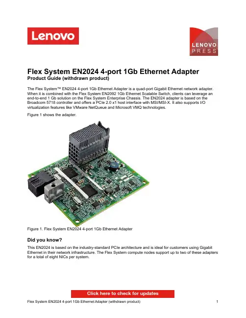
Flex System EN2024 4-port 1Gb Ethernet Adapter Product Guide (withdrawn product)The Flex System™ EN2024 4-port 1Gb Ethernet Adapter is a quad-port Gigabit Ethernet network adapter. When it is combined with the Flex System EN2092 1Gb Ethernet Scalable Switch, clients can leverage an end-to-end 1 Gb solution on the Flex System Enterprise Chassis. The EN2024 adapter is based on the Broadcom 5718 controller and offers a PCIe 2.0 x1 host interface with MSI/MSI-X. It also supports I/O virtualization features like VMware NetQueue and Microsoft VMQ technologies.Figure 1 shows the adapter.Figure 1. Flex System EN2024 4-port 1Gb Ethernet AdapterDid you know?This EN2024 is based on the industry-standard PCIe architecture and is ideal for customers using Gigabit Ethernet in their network infrastructure. The Flex System compute nodes support up to two of these adapters for a total of eight NICs per system.Click here to check for updatesSupported serversThe following table lists the Flex System compute nodes that support the adapters. Table 2. Supported serversDescription Part numberFlex System EN2024 4-port 1Gb Ethernet Adapter49Y7900Y N Y Y Y Y Y Y Y*Y* * Only supported in slots 1 and 2 of the x280 X6, x480 X6, and x880 X6See ServerProven at the following web address for the latest information about the expansion cards that are supported by each blade server type:/servers/eserver/serverproven/compat/us/I/O adapter cards are installed in the slot in supported servers, such as the x240, as highlighted in the following figure.Figure 2. Location of the I/O adapter slots in the Flex System x240 Compute NodeSupported I/O modulesTable 4. Adapter to I/O bay correspondenceI/O adapter slot in the server Port on the adapter Corresponding I/O module bayin the chassisSlot 1Port 1Module bay 1Port 2Module bay 2Port 3*Module bay 1Port 4*Module bay 2 Slot 2Port 1Module bay 3Port 2Module bay 4Port 3*Module bay 3Port 4*Module bay 4Slot 3(full-wide compute nodes only)Port 1Module bay 1 Port 2Module bay 2 Port 3*Module bay 1 Port 4*Module bay 2Slot 4(full-wide compute nodes only)Port 1Module bay 3 Port 2Module bay 4 Port 3*Module bay 3 Port 4*Module bay 4* Ports 3 and 4 require Upgrade 1 of either the EN2092 1Gb or EN4093 10Gb switch. The EN4091 Pass-thru only supports ports 1 and 2 (and only when two I/O modules are installed).The connections between the adapters installed in the compute nodes to the switch bays in the chassis are shown diagrammatically in the following figure. The figure shows both half-wide servers, such as the x240 with two adapters, and full-wide servers, such as the x440 with four adapters.Figure 3. Logical layout of the interconnects between I/O adapters and I/O modulesPopular configurationsThe adapters can be used in various configurations. The following figure shows EN2024 4-port 1Gb Ethernet Adapters installed in both slots of the x240 (a model without the Embedded 10Gb Virtual Fabric Adapter), which in turn is installed in the chassis. The chassis also has four Flex System EN2092 1Gb Ethernet Scalable Switches, each with Upgrade 1 installed to enable 28 internal ports.Figure 4. Example configurationThe following table lists the parts that are used in the configuration.Table 5. Components used when connecting the adapter to the 10 GbE switchesDescription Quantity Partnumber8737-x1x Flex System x240 Compute Node (without Embedded 10Gb Virtual Fabric Adapter) or other1 to 14supported server90Y3554Flex System EN2024 4-port 1Gb Ethernet Adapter 2 perserver 8721-A1x Flex System Enterprise Chassis149Y4294Flex System EN2092 1Gb Ethernet Scalable Switch490Y3562Flex System EN2092 1Gb Ethernet Scalable Switch (Upgrade 1)4 Related publicationsTrademarksLenovo and the Lenovo logo are trademarks or registered trademarks of Lenovo in the United States, other countries, or both. A current list of Lenovo trademarks is available on the Web athttps:///us/en/legal/copytrade/.The following terms are trademarks of Lenovo in the United States, other countries, or both:Lenovo®Flex SystemServerProven®System x®The following terms are trademarks of other companies:Linux® is the trademark of Linus Torvalds in the U.S. and other countries.Microsoft®, Windows Server®, and Windows® are trademarks of Microsoft Corporation in the United States, other countries, or both.Other company, product, or service names may be trademarks or service marks of others.Flex System EN2024 4-port 1Gb Ethernet Adapter (withdrawn product)11。
数字家庭主板M2NDH-支持AMD®SocketAM2Athlon64FX/Athlo64X2/Athlon64/Sempron -AMDLive!™Ready-强大扩充能力:1xPCI-Ex16、2xPCI-E、3xPCI-华硕WiFi-APSolo-华硕DHRemote™-华硕MP3-In™-华硕Q-Connector-高保真音频中央处理器支持AMD®SocketAM2Athlon64FX/Athlo64X2/Athlon64/Sempron 支持AMDCool'n'Quiet™技术AMD64架构,同时兼容32位和64位计算AMDLive!™Ready芯片组NVIDIAnForce®430MCP前端总线2000/1600MT/s内存双通道内存架构4x240-pinDIMM内存插槽,支持最大容量高达8GB的DDR2800/667/533ECC和non-ECC、un-buffered内存扩充插槽1xPCI-Expressx16插槽2xPCI-Expressx1插槽3xPCI2.2插槽存储装置/RAID-1xUltraDMA133/100/66/33-4xSerialATA3.0Gb/s-NVIDIAMediaShield™RAID通过SerialA TA设备支持RAID0、1、0+1、5和JBOD网络功能NVIDIAnForce®430内建GigabitMAC,支持externalAttansicPHY无线局域网:54MbpsIEEE802.11b/g(华硕WiFi-APSolo)音频功能ADI6声道高保真音频CODEC背板S/PDIF数字音频输出USB高达8个USB2.0/1.1接口M2N-VMDH-AMDSocketAM2-NVIDIAGeForce6100/nForce430-双通道DDR2800/667/533-1xPCIExpressx16+1xPCIExpressx1+2xPCI-双VGA:DVI-D和D-Sub-8声道高保真音频-2x1394a接口中央处理器支持AMD®SocketAM2Athlon64X2/Athlon64FX/Athlon64/Sempro nAMDCool'n'Quiet™技术AMD64架构,兼容32位和64位计算AMDLive!™Ready芯片组NVIDIAGeForce6100/nForce430前端总线2000/1600MT/s 内存双通道内存架构4x240-pinDIMM插槽,支持最大容量为8GB的DDR2800/667/533non-ECC,un-buffered内存显卡集成GeForce6100GPU高清晰视频处理,最高分辨率可达1920x1440(@75Hz)支持RGB显示;UXGA1600x1200(@60Hz)支持DVI-D显示支持双VGA输出:DVI-D和RGB注意:DVI-D不能用来输出RGB信号至CRT。
marvell cpu介绍marvell cpu介绍一marvell公司成立于1995年,总部在硅谷,在中国上海设有研发中心,亚太地区包括北京、韩国、台湾这些地方都有技术支持团队。
目前marvell是全球十大无晶片工厂半导体设计公司。
marvell现在每天要运送超过100万片基于arm架构的处理器,这不单单包括手机应用处理器,同时也包括通信处理器、存储、wifi 等芯片。
marvell在2005、2006年底,分别以2400万与6亿美元美元,完成了对ut斯达康系统级芯片(system-on-chip)业务,以及intel xscale手机及手持设备芯片业务的全资收购。
具体到移动终端的话,marvell手机及手持设备业务(chg)方面的pxa系列产品产品,从英特尔的strong arm到pxa 255, pxa 270系列再到marvell的pxa 3xx系列应用处理器,marvell的chg 产品同时具备低功耗和高性能两大特点。
marvell cpu介绍二marvell pxa1908拥有四个cpu核心,主频为1.2ghz,高频版为1.5ghz,支持720p显示以及800万像素摄像头cortex-a53架构,64位低端处理器,28纳米制程。
看到这里就知道,低端货marvell cpu介绍三这两个cpu性能是一样的,cpu部分均为a7架构,主频都是1.2ghz,gpu部分均为gc2000,按理说这cpu性能还是可以的,玩个大游戏什么的不会卡,但是实际用起来由于gpu优化的不好兼容性差一直是公认的,很多主流游戏都无法兼容,所以实际性能还不如mtk6589,但是也这两个cpu也绝对能和普通的a9架构双核有的一拼了至于楼下那位id是neveraspire的傻逼说的话,你就别信了,第一这两个cpu性能完全一模一样,不存在哪个好哪个差的问题,第二gc2000的显卡,性能还是不错的比sgx540都要强,只要能兼容,玩大游戏都不会卡更别说是小游戏,所以那位傻逼说玩小游戏都会卡,真是痴人说梦相关阅读:cpu功能介绍处理指令英文processing instructions;这是指控制程序中指令的执行顺序。

回想调试88E1111芯片时,遇到不少的心酸,花掉不少的money,从目前实现的UDP数据传输,ICMP ping包,ARP包,与大家一起分享一下,也许是受到调试时遇问题发帖求助,到热心网友的帮助的感慨吧;1、芯片Package:我选择的为《117-Pin TFBGA Package》,建议没有调试过以太网的不要选择BGA封装,最好选择PQFP封装,调试过硬件会懂得;2、硬件配置:通过芯片CONFIG[6:0]这7个引脚与外部信号相连接,得到不同的结果,例如传输速率、光线、以太网接口等,通过与外界不同管脚的连接也影响着寄存器,他们分别可以与VSS、LED_TX、LED_RX、LED_DUPLEX、LED_LINK1000、LED_LINK100、LED_LINK10、VDDO连接,依次代表3位从000到111的值;对于CONFIG[6:0]分别对应3位,每位都具有自己的含义,详见下datasheet P65;我选择的千兆以太网的配置为:CONFIG[0]--VSS,CONFIG[1]-- LED_RX,CONFIG[2]-- LED_LINK100,CONFIG[3]-- VSS,CONFIG[4]-- VDDO,CONFIG[5]-- VDDO,CONFIG[6]-- VSS,对照上面以PHY地址为例,有PHYADR为10000b,也可参照手册实例P64;3、MAC接口:通过上一步硬件配置知HWCFG_MODE[3:0]为1111,实际应该先确定传输速率、模式,再选择HWCFG_MODE[3:0]对应的值,参考手册P48,当选定此值时可知为GMII/MII to copper,接下来可以参照P48 GMII MAC接口图;在此不给我实际的原理图,真是有原因的,我原来做硬件时候就是参照别人的图纸做的,做回来的板子有部分好用,部分不好用,由于采用BGA封装,当时就以为是芯片没有焊接好(没用专用BGA焊接机),做了几种板子之后发现奇怪的现象,数据只能读,不能写,其他的一切都正常,猜想过板子使用发热、焊接内部助焊剂没有清洗干净等等,其实就是自己没有看手册,太相信别人的原理图,受先入为主的思想,认为只要好使过的板子原理就没有问题,如果以后遇到调试硬件问题,一定要回答datasheet中寻求答案,大神们早都知道的东西,可我在调试以太网给我上了深深一课,这也就是不给我画好板子原理图的原因,别给大家误导了!一切都得从根本出发!!!4、上拉电阻:一定要注意一些引脚需要上拉电阻,例如:MIC、MDIO、RESET 等引脚;5、电源地信号:88E1111有两种不同的电源2.5V、1.2V,对于2.5V需要区分不同的地方的供电,参照datasheet P73,我只把数字2.5V与模拟2.5V用磁珠分开,将地采用铺地的方式链接到一起;6、以太网网线接口:有的带有变压器,有的没有,这样就需要外加芯片转换,在两者直接转换时一定要对应好引脚,否则在做好硬件后,最起码的LINK都链接不上的。
在连续两个平台的uboot和Linux系统移植过程中,在千兆网口调试这块都遇到了很大的麻烦。
由于寄存器数量庞大,千兆网口MAC和PHY内部结构复杂,MAC和PHY接口种类多,千兆以太网驱动的调试成了系统移植过程中最让人烦心的一个环节。
就像火箭队,每次都让球迷无比揪心,不是输的窝囊,就是伤兵满营,现在新赛季又两连败了,打的比勇士还勇士,后场两个比我还瘦的家伙,怎么防守。
算了,不扯这么多了,今天要说的是网口MAC+PHY的一些原理和代码分析。
(以Freescale的ETSEC和Marvell的88E1111为例。
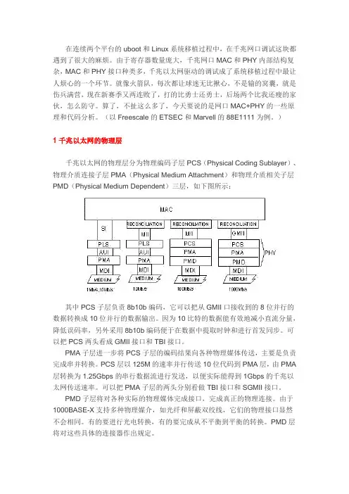
)1 千兆以太网的物理层千兆以太网的物理层分为物理编码子层PCS(Physical Coding Sublayer)、物理介质连接子层PMA(Physical Medium Attachment)和物理介质相关子层PMD(Physical Medium Dependent)三层,如下图所示:其中PCS子层负责8b10b编码,它可以把从GMII口接收到的8位并行的数据转换成10位并行的数据输出。
因为10比特的数据能有效地减小直流分量,降低误码率,另外采用8b10b编码便于在数据中提取时钟和进行首发同步。
可以把PCS两头看成GMII接口和TBI接口。
PMA子层进一步将PCS子层的编码结果向各种物理媒体传送,主要是负责完成串并转换。
PCS层以125M的速率并行传送10位代码到PMA层,由PMA 层转换为1.25Gbps的串行数据流进行发送,以便实际能得到1Gbps的千兆以太网传送速率。
可以把PMA子层的两头分别看做TBI接口和SGMII接口。
PMD子层将对各种实际的物理媒体完成接口,完成真正的物理连接。
由于1000BASE-X支持多种物理媒介,如光纤和屏蔽双绞线,它们的物理接口显然不会相同。
有的要进行光电转换,有的要完成从不平衡到平衡的转换。
PMD层将对这些具体的连接器作出规定。
2 Freescale 的ETSEC与PHY之间的接口Freescale的MPC8314和P2020都自带了三速以太网控制器ETSEC,可以提供10M,100M,1000M三种速率的接口。
千兆以太网芯片88E1111 RGMII模式的驱动88E1111可工作在10Mb/s,100Mb/s,1000Mb/s下,由于DE2-115开发板在设计的时候只采用了4位数据端口,因此只能采用MII模式(100Mb/s),或者RGMII模式(1000Mb/s),看了官方的DATASHEET后,几乎得到什么,于是就想到了一个办法,就是将官方所给的关于RGMII的例程下到开发板上,然后将88E1111的配置寄存器里面的数据用NIOS II读出来,这样就获得了正确的配置数据,然后就将配置数据用NIOS II 配置给芯片,然后就遇到了很奇怪的事情:当我把配置的那几行代码都注释掉以后居然88E1111还可以继续正常运行,后来发现,只要给芯片的硬复位引脚Reset_n一个较长的复位即可,大概10~20ms就可以了。
具体如何将芯片通过CONFIG引脚配置成RGMII 模式,可以参考DE2-115的原理图。
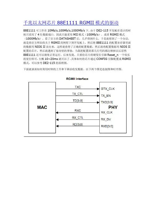
下面就谈谈如何利用时钟的上升和下降沿收发数据。
以下两个图是连接图和时序图。
先谈输出端Tx:Tx端有三个信号,Txd_RGM,Tx_ctrl,Tx_clk,其中Tx_clk是由FPGA提供的125MHz 的时钟,Tx_RGM是发送的数据,Tx_ctrl在Tx_clk时钟上升沿发送的是Tx_en,在下降沿发送的是Tx_en和Tx_er的异或值。
Rx端也有三个信号:Rxd_RGM,Rx_ctrl,Rx_clk,其中Rx_clk是由88E1111提供的125MHz的时钟,Rx_RGM表示接收到的数据,Rx_ctrl在Rx_clk的上升沿收到的是Rx_en,在下降沿收到的是Rx_en和Rx_er的异或值。
由于一个always模块中不能同时使用时钟的上升和下降沿,可以调用DDIO模块,当然,也可以不用,下图就是不采用DDIO的一个示意图,这个是用来设计DDR SDRAM的,可以借鉴module rgmii_io(input Tx_clk,input Rx_clk,output Tx_clk_RGM,input[7:0] Txd,output [3:0] Txd_RGM,input Tx_en,input Tx_er,output Tx_ctrl,input[3:0] Rxd_RGM,output reg[7:0] Rxd,input Rx_ctrl,output reg Rx_dv,output reg Rx_er);assign Tx_clk_RGM = ~Tx_clk;//******************************************************************************//Tx control //******************************************************************************wire Tx_err;reg[3:0] Txd_low,Txd_high;reg Tx_en_d1,Tx_err_d1;assign Tx_err=Tx_en^Tx_er;assign Txd_RGM = Tx_clk ? Txd_low : Txd_high;assign Tx_ctrl = Tx_clk ? Tx_en_d1 : Tx_err_d1;always@(posedge Tx_clk)beginTxd_low <= Txd[3:0];Txd_high <= Txd[7:4];Tx_en_d1 <= Tx_en;Tx_err_d1 <= Tx_err;end//******************************************************************************//Rx control //******************************************************************************wire Rx_er_d1;reg[3:0] Rxd_low,Rxd_high;reg Rx_dv_d1,Rx_err_d1,Rx_dv_d2,Rx_er_d2;reg[7:0] Rxd_d1;assign Rx_er_d1=Rx_dv_d1^Rx_err_d1;wire Rx_clk_n;assign Rx_clk_n=~Rx_clk;always@(posedge Rx_clk_n)beginRxd_low<=Rxd_RGM;Rx_dv_d1<=Rx_ctrl;endalways@(posedge Rx_clk)beginRxd_high<=Rxd_RGM;Rx_err_d1<=Rx_ctrl;endalways@(posedge Rx_clk_n)beginRxd_d1<={Rxd_high,Rxd_low};Rx_dv_d2<=Rx_dv_d1;Rx_er_d2<=Rx_er_d1;endalways@(posedge Rx_clk)beginRxd<=Rxd_d1;Rx_dv<=Rx_dv_d2;Rx_er<=Rx_er_d2;end。
浮思特科技FST50_04E WiFi模组硬件规格书版本4.0本文介绍FST50_04E的产品硬件规格发布说明版本发布说明日期V1.0首次发布2019年4月9日V2.0更改Pin引脚定义2019年10月16日V3.0更改Pin引脚定义,外设参考电路图更改2020年3月4日V4.0Pin引脚功能完善,更新参考原理图,更新模组生产保质,联系方式变更2020年7月22日免责申明和版权公告本文中的信息,包括供参考的URL地址,如有变更,恕不另行通知。
文档“按现状”提供,不负任何担保责任,包括对适销性、适用于特定用途或非侵权性的任何担保,和任何提案、规格或样品在他处提到的任何担保。
本文档不负任何责任,包括使用本文档内信息产生的侵犯任何专利权行为的责任。
本文档在此未以禁止反言或其他方式授予任何知识产权使用许可,不管是明示许可还是暗示许可。
由于产品版本升级或其他原因,本文档内容有可能变更。
深圳市浮思特科技有限公司保留在没有任何通知或者提示的情况下对本文档的内容进行修改的权利。
另本文档仅作为使用指导,不确保文档内容完全没有错误,本文档中的所有陈述、信息和建议也不构成任何明示或暗示的担保。
Wi-Fi联盟成员标志归Wi-Fi联盟所有。
文中提到的所有商标名称、商标和注册商标均属其各自所有者的财产,特此声明。
本文档版权归深圳市浮思特科技有限公司所有,保留所有权利。
目录目录 (4)1.产品概述 (5)1.1特性 (5)1.2芯片框架 (6)2.模组参数 (6)2.1模组详细参数 (6)2.2RF参数范围 (7)3.模组引脚说明 (8)3.1模组引脚分布图 (8)3.2模组引脚说明 (8)4.外型与尺寸 (9)5数字端口特征 (10)6.功耗 (10)7.倾斜升温 (10)8.模组摆放指南 (11)9.WIFI模组外设参考电路图 (13)10.模组型号介绍 (13)11.模组生产保质 (14)12.包装 (15)13.联系方式 (15)1.产品概述FST50_04E是浮思特科技采用翱捷科技(上海)有限公司的ASR5502A芯片研发的高集成、高性能、低成本WIFI模组,ASR5502A集成了射频收发机、802.11PHY+MAC、ARM Cortex-M4F、API接口、实时计数器(RTC)和完整的电源管理电路。
Marvell.Moving Forward FasterDoc. No. MV-S105540-00, Rev. --March 4, 2009Document Classification: Proprietary Information88E1111 Product BriefIntegrated 10/100/1000 Ultra Gigabit Ethernet TransceiverDocument ConventionsNote: Provides related information or information of special importance.Caution: Indicates potential damage to hardware or software, or loss of data.Warning: Indicates a risk of personal injury.Document StatusAdvance Information This document contains design specifications for initial product development. Specifications may change without notice. Contact Marvell Field Application Engineers for more information.Preliminary InformationThis document contains preliminary data, and a revision of this document will be published at a later date. Specifications may change without notice. Contact Marvell Field Application Engineers for more information.Final Information This document contains specifications on a product that is in final release. Specifications may change without notice. Contact Marvell Field Application Engineers for more information.Doc Status: AdvanceTechnical Publications: 1.00For more information, visit our website at: DisclaimerNo part of this document may be reproduced or transmitted in any form or by any means, electronic or mechanical, including photocopying and recording, for any purpose, without the express written permission of Marvell. Marvell retains the right to make changes to this document at any time, without notice. Marvell makes no warranty of any kind, expressed or implied, with regard to any information contained in this document, including, but not limited to, the implied warranties of merchantability or fitness for any particular purpose. Further, Marvell does not warrant the accuracy or completeness of the information, text, graphics, or other items contained within this document. Marvell products are not designed for use in life-support equipment or applications that would cause a life-threatening situation if any such products failed. Do not use Marvell products in these types of equipment or applications.With respect to the products described herein, the user or recipient, in the absence of appropriate U.S. government authorization, agrees:1) Not to re-export or release any such information consisting of technology, software or source code controlled for national security reasons by the U.S. Export Control Regulations ("EAR"), to a national of EAR Country Groups D:1 or E:2;2) Not to export the direct product of such technology or such software, to EAR Country Groups D:1 or E:2, if such technology or software and direct products thereof are controlled for national security reasons by the EAR; and,3) In the case of technology controlled for national security reasons under the EAR where the direct product of the technology is a complete plant or component of a plant, not to export to EAR Country Groups D:1 or E:2 the direct product of the plant or major component thereof, if such direct product is controlled for national security reasons by the EAR, or is subject to controls under the U.S. Munitions List ("USML").At all times hereunder, the recipient of any such information agrees that they shall be deemed to have manually signed this document in connection with their receipt of any such information.Copyright © 2009. Marvell International Ltd. All rights reserved. Marvell, the Marvell logo, Moving Forward Faster, Alaska, Fastwriter, Datacom Systems on Silicon, Libertas, Link Street, NetGX, PHYAdvantage, Prestera, Raising The Technology Bar, The Technology Within, Virtual Cable Tester, and Yukon are registered trademarks of Marvell. Ants, AnyVoltage, Discovery, DSP Switcher, Feroceon, GalNet, GalTis, Horizon, Marvell Makes It All Possible, RADLAN, UniMAC, and VCT are trademarks of Marvell. All other trademarks are the property of their respective owners.88E1111 Product BriefIntegrated 10/100/1000 Ultra Gigabit Ethernet TransceiverDoc. No. MV-S105540-00 Rev. -- Copyright © 2009 Marvell Page 2Document Classification: Proprietary InformationMarch 4, 2009, Advance88E1111 Product BriefIntegrated 10/100/1000 Ultra Gigabit Ethernet TransceiverCopyright © 2009 MarvellDoc. No. MV-S105540-00, Rev. --March 4, 2009, AdvanceDocument Classification: Proprietary InformationPage 3O VERVIEWThe Alaska ® Ultra 88E1111 Gigabit Ethernet Trans-ceiver is a physical layer device for Ethernet1000BASE-T, 100BASE-TX, and 10BASE-T applica-tions. It is manufactured using standard digital CMOS process and contains all the active circuitry required to implement the physical layer functions to transmit and receive data on standard CAT 5 unshielded twisted pair.The 88E1111 device incorporates the Marvell Virtual Cable Tester ® (VCT™) feature, which uses TimeDomain Reflectometry (TDR) technology for the remote identification of potential cable malfunctions, thus reducing equipment returns and service calls. Using VCT, the Alaska 88E1111 device detects and reports potential cabling issues such as pair swaps, pair polar-ity and excessive pair skew. The device will also detect cable opens, shorts or any impedance mismatch in the cable and report accurately within one meter the dis-tance to the fault.The 88E1111 device supports the Gigabit Media Inde-pendent Interface (GMII), Reduced GMII (RGMII), Serial Gigabit Media Independent Interface (SGMII), the Ten-Bit Interface (TBI), and Reduced TBI (RTBI) for direct connection to a MAC/Switch port.The 88E1111 device incorporates an optional 1.25 GHz SERDES (Serializer/Deserializer). The serial interface may be connected directly to a fiber-optic transceiver for 1000BASE-T/1000BASE-X media conversion appli-cations. Additionally, the 88E1111 device may be used to implement 1000BASE-T Gigabit Interface Converter (GBIC) or Small Form Factor Pluggable (SFP) modules.The 88E1111 device uses advanced mixed-signal pro-cessing to perform equalization, echo and crosstalk cancellation, data recovery, and error correction at a gigabit per second data rate. The device achievesrobust performance in noisy environments with very low power dissipation.The 88E1111 device is offered in three different pack-age options including a 117-Pin TFBGA, a 96-pin BCC featuring a body size of only 9 x 9 mm, and a 128 PQFP package.F EATURES•10/100/1000BASE-T IEEE 802.3 compliant •Supports GMII, TBI, reduced pin count GMII(RGMII), reduced pin count TBI (RTBI), and serial GMII (SGMII) interfaces•Integrated 1.25 GHz SERDES for 1000BASE-X fiber applications •Four RGMII timing modes•Energy Detect and Energy Detect+ low power modes•Three loopback modes for diagnostics•“Downshift” mode for two-pair cable installations •Fully integrated digital adaptive equalizers, echo cancellers, and crosstalk cancellers •Advanced digital baseline wander correction •Automatic MDI/MDIX crossover at all speeds of operation•Automatic polarity correction•IEEE 802.3u compliant Auto-Negotiation•Software programmable LED modes including LED testing•Automatic detection of fiber or copper operation •Supports IEEE 1149.1 JTAG•Two-Wire Serial Interface (TWSI) and MDC/MDIO •CRC checker, packet counter •Packet generation •Virtual Cable Tester (VCT)•Auto-Calibration for MAC Interface outputs •Requires only two supplies: 2.5V and 1.0V (with 1.2V option for the 1.0V supply)•I/Os are 3.3V tolerant•Low power dissipation Pave = 0.75W •117-Pin TFBGA, 96-Pin BCC, and 128 PQFP package options•117-Pin TFBGA and 96-Pin BCC packages avail-able in Commercial or Industrial grade •RoHS 6/6 compliant packages available88E1111 Product BriefIntegrated 10/100/1000 Ultra Gigabit Ethernet TransceiverDoc. No. MV-S105540-00, Rev. -- Copyright © 2009 Marvell Page 4Document Classification: Proprietary InformationMarch 4, 2009, Advance88E1111 Device used in Copper Application88E1111 Device used in Fiber Application88E1111 RGMII/GMII MAC to SGMII MAC ConversionTable of Contents1.1117-Pin TFBGA Package (6)1.2 96-Pin BCC Package (7)1.3128-Pin PQFP Package (8)1.4Pin Description (9)1.4.1Pin Type Definitions (9)1.5I/O State at Various Test or Reset Modes (33)1.6117-Pin TFBGA Pin Assignment List - Alphabetical by Signal Name (34)1.796-Pin BCC Pin Assignment List - Alphabetical by Signal Name (36)1.8128-Pin PQFP Pin Assignment List - Alphabetical by Signal Name (38)2.1117-pin TFBGA Package (40)2.296-pin BCC Package - Top View (42)2.396-Pin BCC Package - Bottom View (43)2.4128-Pin PQFP Package (44)3.1Ordering Part Numbers and Package Markings (45)3.1.1RoHS 5/6 Compliant Marking Examples (46)3.1.2RoHS 6/6 Compliant Marking Examples (49)Copyright © 2009 Marvell Doc. No. MV-S105540-00, Rev. --March 4, 2009, Advance Document Classification: Proprietary Information Page 588E1111 Product BriefIntegrated 10/100/1000 Ultra Gigabit Ethernet TransceiverDoc. No. MV-S105540-00, Rev. -- Copyright © 2009 Marvell Page 6Document Classification: Proprietary InformationMarch 4, 2009, AdvanceSection 1. Signal DescriptionThe 88E1111 device is a 10/100/1000BASE-T/1000BASE-X Gigabit Ethernet transceiver.1.1117-Pin TFBGA PackageFigure 1:88E1111 Device 117-Pin TFBGA Package (Top View)Figure 2:Pin A1 Location123456789A RXD5RXD6S_IN+S_IN-S_CLK+S_CLK-S_OUT+S_OUT-LED_LINK1000AB RX_DV RXD0RXD3VDDO CRS COL AVDD LED_LINK100VDDOHBC RX_CLK VDDO RXD2RXD4RXD7DVDD DVDD LED_LINK10LED_RX CD TX_CLK RX_ER RXD1VSS VSS VSS DVDD CONFIG[0]LED_TX DE TX_EN GTX_CLK DVDD VSS VSS VSS DVDD LED_DUPLEX CONFIG[1]EF TXD0TX_ER DVDD VSS VSS VSS VDDOH CONFIG[2]CONFIG[4]FG NC TXD1TXD2VSS VSS VSS CONFIG[3]CONFIG[6]CONFIG[5]GH TXD4TXD3TXD5VSS VSS VSS VSSC SEL_FREQ XTAL1HJ TXD6TXD7DVDD VSS VSS VSS DVDD VDDOHXTAL2JK VDDO 125CLK RESETn VSS VSS VSS NC TDO VDDOX KL INTn VDDOX MDC COMA VSS VSS TDI TMS TCK LM MDIO RSET AVDD AVDD HSDAC+HSDAC-AVDD AVDD TRSTn MN MDI[0]+MDI[0]-MDI[1]+MDI[1]-AVDD MDI[2]+MDI[2]-MDI[3]+MDI[3]-N12345678988E1111-BABSignal Description96-Pin BCC Package1.2 96-Pin BCC PackageFigure 3:88E1111 Device 96-Pin BCC Package (Top View)88E1111 - CAACopyright © 2009 Marvell Doc. No. MV-S105540-00, Rev. --March 4, 2009, Advance Document Classification: Proprietary Information Page 788E1111 Product BriefIntegrated 10/100/1000 Ultra Gigabit Ethernet TransceiverDoc. No. MV-S105540-00, Rev. --Copyright © 2009 Marvell Page 8Document Classification: Proprietary InformationMarch 4, 2009, Advance1.3128-Pin PQFP PackageFigure 4:88E1111 Device 128-Pin PQFP Package (Top View)78910111213141516171819202122232425262728293031323388E1111 - RCJTop ViewR X _C L K R X _E R V S S T X _C L K V D D O D V D D T X _E R G T X _C L K V S S T X _E N D V D D T X D 0T X D 1T X D 2V S S V S S D V D D T X D 3T X D 4T X D 5D V D D T X D 6T X D 7V D D O 125C L K I N T n M D I OSignal DescriptionPin Description1.4Pin Description1.4.1Pin Type DefinitionsPin Type DefinitionH Input with hysteresisI/O Input and outputI Input onlyO Output onlyPU Internal pull upPD Internal pull downD Open drain outputZ Tri-state outputmA DC sink capabilityCopyright © 2009 Marvell Doc. No. MV-S105540-00, Rev. --March 4, 2009, Advance Document Classification: Proprietary Information Page 988E1111 Product BriefIntegrated 10/100/1000 Ultra Gigabit Ethernet TransceiverDoc. No. MV-S105540-00, Rev. --Copyright © 2009 Marvell Page 10Document Classification: Proprietary InformationMarch 4, 2009, AdvanceTable 1:Media Dependent Interface117-TFBGA Pin #96-BCC Pin #128-PQFP Pin #Pin Name Pin TypeDescriptionN1N229314142MDI[0]+MDI[0]-I/O, DMedia Dependent Interface[0].In 1000BASE-T mode in MDI configuration, MDI[0]± correspond to BI_DA±.In MDIX configuration, MDI[0]± correspond to BI_DB±.In 100BASE-TX and 10BASE-T modes in MDI configuration, MDI[0]± are used for the transmit pair. In MDIX configuration, MDI[0]± are used for the receive pair. MDI[0]± should be tied to ground if not used.N3N433344647MDI[1]+MDI[1]-I/O, D Media Dependent Interface[1].In 1000BASE-T mode in MDI configuration, MDI[1]± correspond to BI_DB±.In MDIX configuration, MDI[1]± correspond to BI_DA±.In 100BASE-TX and 10BASE-T modes in MDI configuration, MDI[1]± are used for the receive pair. In MDIX configuration, MDI[1]± are used for the transmit pair.MDI[1]± should be tied to ground if not used.N6 N739415657MDI[2]+MDI[2]-I/O, D Media Dependent Interface[2].In 1000BASE-T mode in MDI configuration,MDI[2]±correspond to BI_DC±.In MDIX configuration, MDI[2]± correspondsto BI_DD±.In 100BASE-TX and 10BASE-T modes,MDI[2]±are not used.MDI[2]± should be tied to ground if not used.N8 N942436162MDI[3]+MDI[3]-I/O, D Media Dependent Interface[3].In 1000BASE-T mode in MDI configuration,MDI[3]± correspond to BI_DD±.In MDIX configuration, MDI[3]± correspondto BI_DC±.In 100BASE-TX and 10BASE-T modes,MDI[3]± are not used.MDI[3]± should be tied to ground if not used.Table 1:Media Dependent Interface (Continued)117-TFBGA Pin #96-BCCPin #128-PQFPPin #Pin Name PinTypeDescriptionCopyright © 2009 Marvell Doc. No. MV-S105540-00, Rev. --Integrated 10/100/1000 Ultra Gigabit Ethernet TransceiverDoc. No. MV-S105540-00, Rev. -- Copyright © 2009 Marvell The GMII interface supports both 1000BASE-T and 1000BASE-X modes of operation. The GMII interface pins are also used for the TBI interface. See Table 3 for TBI pin definitions. The MAC interface pins are 3.3V tolerant. Table 2:GMII/MII Interfaces117-TFBGA Pin #96-BCC Pin #128-PQFP Pin #Pin Name PinTypeDescriptionE2814GTX_CLKIGMII Transmit Clock. GTX_CLK provides a 125 MHz clock reference for TX_EN, TX_ER, and TXD[7:0]. This clock can be stopped when the device is in 10/100BASE-T modes, and also during Auto-Negotiation.D1410TX_CLK O, ZMII Transmit Clock. TX_CLK provides a 25 MHz clock reference for TX_EN, TX_ER, and TXD[3:0] in 100BASE-TX mode, and a 2.5 MHz clock reference in 10BASE-T mode.TX_CLK provides a 25 MHz, 2.5 MHz, or 0 MHz clock during 1000 Mbps Good Link, Auto-Negotiation, and Link Lost statesdepending on the setting of register 20.6:4.The 2.5 MHz clock is the default rate, which may be programmed to another frequency by writing to register 20.6:4.E1916TX_EN IGMII and MII Transmit Enable. In GMII/MII mode when TX_EN is asserted, data on TXD[7:0] along with TX_ER is encoded and transmitted onto the cable.TX_EN is synchronous to GTX_CLK, and synchronous to TX_CLK in 100BASE-TX and 10BASE-T modes.F2713TX_ER IGMII and MII Transmit Error. In GMII/MII mode when TX_ER and TX_EN are both asserted, the transmit error symbol is trans-mitted onto the cable. When TX_ER is asserted with TX_EN de-asserted, carrier extension symbol is transmitted onto the cable.TX_ER is synchronous to GTX_CLK, and synchronous to TX_CLK in 100BASE-TX and 10BASE-T modes.Copyright © 2009 Marvell Doc. No. MV-S105540-00, Rev. --J2J1H3H1H2G3G2F120191817161412112928262524201918TXD[7]TXD[6]TXD[5]TXD[4]TXD[3]/TXD[3]TXD[2]/TXD[2]TXD[1]/TXD[1]TXD[0]/TXD[0]IGMII and MII Transmit Data. In GMII mode, TXD[7:0] present the data byte to be trans-mitted onto the cable in 1000BASE-T mode. In MII mode, TXD[3:0] present the data nib-ble to be transmitted onto the cable in 100BASE-TX and 10BASE-T modes. TXD[7:4] are ignored in these modes, but should be driven either high or low. These pins must not float.TXD[7:0] are synchronous to GTX_CLK, and synchronous to TX_CLK in 100BASE-TX and 10BASE-T modes.Inputs TXD[7:4] should be tied low if not used (e.g., RGMII mode).C127RX_CLK O, ZGMII and MII Receive Clock. RX_CLK pro-vides a 125 MHz clock reference for RX_DV, RX_ER, and RXD[7:0] in 1000BASE-T mode, a 25 MHz clock reference in100BASE-TX mode, and a 2.5 MHz clock reference in 10BASE-T mode.TX_TCLK comes from the RX_CLK pins used in jitter testing. Refer to Register 9 for jitter test modes.B1944RX_DV O, ZGMII and MII Receive Data Valid. When RX_DV is asserted, data received on the cable is decoded and presented on RXD[7:0] and RX_ER.RX_DV is synchronous to RX_CLK.D238RX_ER O, ZGMII and MII Receive Error. When RX_ER and RX_DV are both asserted, the signals indicate an error symbol is detected on the cable.When RX_ER is asserted with RX_DV de-asserted, a false carrier or carrier extension symbol is detected on the cable. RX_ER is synchronous to RX_CLK.Table 2:GMII/MII Interfaces (Continued)117-TFBGA Pin #96-BCC Pin #128-PQFP Pin #Pin Name Pin TypeDescriptionIntegrated 10/100/1000 Ultra Gigabit Ethernet TransceiverDoc. No. MV-S105540-00, Rev. --Copyright © 2009 Marvell C5A2A1C4B3C3D3B286878990919392951201211231241251261283RXD[7]RXD[6]RXD[5]RXD[4]RXD[3]/RXD[3]RXD[2]/RXD[2]RXD[1]/RXD[1]RXD[0]/RXD[0]O, ZGMII and MII Receive Data. Symbolsreceived on the cable are decoded and pre-sented on RXD[7:0] in 1000BASE-T mode. In MII mode, RXD[3:0] are used in100BASE-TX and 10BASE-T modes. In MII mode, RXD[7:4] are driven low. RXD[7:0] is synchronous to RX_CLK.B584115CRSO, ZGMII and MII Carrier Sense. CRS asserts when the receive medium is non-idle. In half-duplex mode, CRS is also asserted during transmission. CRS assertion during half-duplex transmit can be disabled by program-ming register 16.11 to 0.CRS is asynchronous to RX_CLK, GTX_CLK, and TX_CLK.B683114COL O, ZGMII and MII Collision. In 10/100/1000BASE-T full-duplex modes, COL is always low. In 10/100/1000BASE-T half-duplex modes, COL asserts only when both the transmit and receive media are non-idle. In 10BASE-T half-duplex mode, COL is asserted to indicate signal quality error(SQE). SQE can be disabled by clearing reg-ister 16.2 to zero.COL is asynchronous to RX_CLK, GTX_CLK, and TX_CLK.Table 2:GMII/MII Interfaces (Continued)117-TFBGA Pin #96-BCC Pin #128-PQFP Pin #Pin Name Pin TypeDescriptionThe TBI interface supports 1000BASE-T mode of operation. The TBI interface uses the same pins as the GMII interface. The MAC interface pins are 3.3V tolerant.Table 3:TBI Interface117-TFBGA Pin #96-BCCPin #128-PQFPPin #Pin Name PinTypeDescriptionE2814GTX_CLK/TBI_TXCLK I TBI Transmit Clock. In TBI mode, GTX_CLKis used as TBI_TXCLK. TBI_TXCLK is a 125MHz transmit clock.TBI_TXCLK provides a 125 MHz clock refer-ence for TX_EN, TX_ER, and TXD[7:0].D1410TX_CLK/RCLK1O, Z TBI 62.5 MHz Receive Clock- even codegroup. In TBI mode, TX_CLK is used asRCLK1.J2 J1 H3 H1 H2 G3 G2 F120191817161412112928262524201918TXD[7]TXD[6]TXD[5]TXD[4]TXD[3]TXD[2]TXD[1]TXD[0]I TBI Transmit Data. TXD[7:0] presents thedata byte to be transmitted onto the cable.TXD[9:0] are synchronous to GTX_CLK.Inputs TXD[7:4] should be tied low if notused (e.g., RTBI mode).E1916TX_EN/TXD8I TBI Transmit Data. In TBI mode, TX_EN isused as TXD8.TXD[9:0] are synchronous to GTX_CLK.F2713TX_ER/TXD9I TBI Transmit Data. In TBI mode, TX_ER isused as TXD9.TXD[9:0] are synchronous to GTX_CLK.TX_ER should be tied low if not used (e.g.,RTBI mode).C127RX_CLK/RCLK0O, Z TBI 62.5 MHz Receive Clock- odd code group. In the TBI mode, RX_CLK is usedas RCLK0.C5 A2 A1 C4 B3 C3 D3 B286878990919392951201211231241251261283RXD[7]RXD[6]RXD[5]RXD[4]RXD[3]RXD[2]RXD[1]RXD[0]O, Z TBI Receive Data code group [7:0]. In theTBI mode, RXD[7:0] present the data byte tobe transmitted to the MAC. Symbolsreceived on the cable are decoded and pre-sented on RXD[7:0].RXD[7:0] are synchronous to RCLK0 andRCLK1.B1944RX_DV/RXD8O, Z TBI Receive Data code group bit 8. In the TBI mode, RX_DV is used as RXD8.RXD[9:0] are synchronous to RCLK0 andRCLK1.Copyright © 2009 Marvell Doc. No. MV-S105540-00, Rev. --Integrated 10/100/1000 Ultra Gigabit Ethernet TransceiverDoc. No. MV-S105540-00, Rev. -- Copyright © 2009 Marvell D238RX_ER/RXD9O, ZTBI Receive Data code group bit 9. In the TBI mode, RX_ER is used as RXD9. RXD[9:0] are synchronous to RCLK0 and RCLK1.B584115CRS/COMMA O, Z TBI Valid Comma Detect. In the TBI mode, CRS is used as COMMA.B683114COL/LPBKITBI Mode Loopback. In the TBI mode, COL is used to indicate loopback on the TBI. When a “0 - 1" transition is sampled on this pin, bit 0.14 is set to 1.When a “1 - 0" is sampled on this pin, bit 0.14 is reset to 0.If this feature is not used, the COL pinshould be driven low on the board. This pin should not be left floating in TBI mode.Table 3:TBI Interface (Continued)117-TFBGA Pin #96-BCC Pin #128-PQFP Pin #Pin Name PinTypeDescriptionThe RGMII interface supports 10/100/1000BASE-T and 1000BASE-X modes of operation.The RGMII interface pins are also used for the RTBI interface. See Table5 for RTBI pin definitions. The MAC interface pins are 3.3V tolerant.Table 4:RGMII Interface117-TFBGA Pin #96-BCCPin #128-PQFPPin #Pin Name PinTypeDescriptionE2814GTX_CLK/TXC I RGMII Transmit Clock provides a 125 MHz,25 MHz, or 2.5 MHz reference clock with ±50 ppm tolerance depending on speed. InRGMII mode, GTX_CLK is used as TXC.H2 G3 G2 F11614121124201918TXD[3]/TD[3]TXD[2]/TD[2]TXD[1]/TD[1]TXD[0]/TD[0]I RGMII Transmit Data. In RGMII mode,TXD[3:0] are used as TD[3:0].In RGMII mode, TXD[3:0] run at double datarate with bits [3:0] presented on the risingedge of GTX_CLK, and bits [7:4] presentedon the falling edge of GTX_CLK. In thismode, TXD[7:4] are ignored.In RGMII 10/100BASE-T modes, the trans-mit data nibble is presented on TXD[3:0] onthe rising edge of GTX_CLK.E1916TX_EN/TX_CTL I RGMII Transmit Control. In RGMII mode,TX_EN is used as TX_CTL. TX_EN is pre-sented on the rising edge of GTX_CLK.A logical derivative of TX_EN and TX_ER ispresented on the falling edge of GTX_CLK.C127RX_CLK/RXC O, Z RGMII Receive Clock provides a 125 MHz,25 MHz, or 2.5 MHz reference clock with ±50 ppm tolerance derived from the receiveddata stream depending on speed. In RGMIImode, RX_CLK is used as RXC.B1944RX_DV/RX_CTL O, Z RGMII Receive Control. In RGMII mode,RX_DV is used as RX_CTL. RX_DV is pre-sented on the rising edge of RX_CLK.A logical derivative of RX_DV and RX_ER ispresented on the falling edge of RX_CLK.B3 C3 D3 B2919392951251261283RXD[3]/RD[3]RXD[2]/RD[2]RXD[1]/RD[1]RXD[0]/RD[0]O, Z RGMII Receive Data. In RGMII mode,RXD[3:0] are used as RD[3:0]. In RGMIImode, RXD[3:0] run at double data rate withbits [3:0] presented on the rising edge ofRX_CLK, and bits [7:4] presented on the fall-ing edge of RX_CLK. In this mode, RXD[7:4]are ignored.In RGMII 10/100BASE-T modes, the receivedata nibble is presented on RXD[3:0] on therising edge of RX_CLK.RXD[3:0] are synchronous to RX_CLK.Copyright © 2009 Marvell Doc. No. MV-S105540-00, Rev. --Integrated 10/100/1000 Ultra Gigabit Ethernet TransceiverDoc. No. MV-S105540-00, Rev. -- Copyright © 2009 Marvell The RTBI interface supports 1000BASE-T mode of operation. The RTBI interface uses the same pins as the RGMII interface. The MAC interface pins are 3.3V tolerant. Table 5:RTBI Interface117-TFBGA Pin #96-BCC Pin #128-PQFP Pin #Pin Name PinTypeDescriptionE2814GTX _CLK/TXC IRGMII Transmit Clock provides a 125 MHz reference clock with ± 50 ppm tolerance. In RTBI mode, GTX_CLK is used as TXC. H2G3G2F11614121124201918TXD[3]/TD[3]TXD[2]/TD[2]TXD[1]/TD[1]TXD[0]/TD[0]IRTBI Transmit Data.In RTBI mode, TXD[3:0] are used asTD[3:0]. TD[3:0] run at double data rate with bits [3:0] presented on the rising edge of GTX_CLK, and bits [8:5] presented on the falling edge of GTX_CLK. In this mode, TXD[7:4] are ignored.E1916TX_EN/TD4_TD9IRTBI Transmit Data.In RTBI mode, TX_EN is used as TD4_TD9. TD4_TD9 runs at a double data rate with bit 4 presented on the rising edge of GTX_CLK, and bit 9 presented on the falling edge of GTX_CLK.C127RX_CLK/RXCO, ZRTBI Receive Clock provides a 125 MHz ref-erence clock with ± 50 ppm tolerance derived from the received data stream. In RTBI mode, RX_CLK is used as RXC.B3C3D3B2919392951251261283RXD[3]/RD[3]RXD[2]/RD[2]RXD[1]/RD[1]RXD[0]/RD[0]O, ZRTBI Receive Data.In RTBI mode, RXD[3:0] are used as RD[3:0]. RD[3:0] runs at double data rate with bits [3:0] presented on the rising edge of RX_CLK, and bits [8:5] presented on the fall-ing edge of RX_CLK. In this mode, RXD[7:4] are ignored.B1944RX_DV/RD4_RD9O, ZRTBI Receive Data.In RTBI mode, RX_DV is used asRD4_RD9. RD4_RD9 runs at a double data rate with bit 4 presented on the rising edge of RX_CLK, and bit 9 presented on the fall-ing edge of RX_CLK.Table 6:SGMII Interface117-TFBGA Pin #96-BCCPin #128-PQFPPin #Pin Name PinTypeDescriptionA3 A48281113112S_IN+S_IN-I SGMII Transmit Data. 1.25 GBaud input -Positive and Negative.Input impedance on the S_IN± pins may beprogrammed for 50 ohm or 75 ohm imped-ance by setting register 26.6. The inputimpedance default setting is determined bythe 75/50 OHM configuration pin.A5 A67980110109S_CLK+S_CLK-I/O SGMII 625 MHz Receive Clock.For Serial Interface modes(HWCFG_MODE[3:0] = 1x00) the S_CLK±pins become Signal Detect± (SD±) inputs.A7 A87775107105S_OUT+S_OUT-O, Z SGMII Receive Data. 1.25 GBaud output -Positive and Negative.Output impedance on the S_OUT± pins maybe programmed for 50 ohm or 75 ohmimpedance by setting register 26.5. Outputamplitude can be adjusted via register26.2:0. The output impedance default settingis determined by the 75/50 OHM configura-tion pin.Copyright © 2009 Marvell Doc. No. MV-S105540-00, Rev. --Integrated 10/100/1000 Ultra Gigabit Ethernet TransceiverDoc. No. MV-S105540-00, Rev. --Copyright © 2009 Marvell Table 7: 1.25 GHz Serial High Speed Interface117-TFBGA Pin #96-BCC Pin #128-PQFP Pin #Pin Name Pin TypeDescriptionA3A48281113112S_IN+S_IN-I1.25 GHz input - Positive and Negative. When this interface is used as a MAC inter-face, the MAC transmitter’s positive output connects to the S_IN+. The MAC transmit-ter’s negative output connects to the S_IN-. When this interface is used as a fiber inter-face, the fiber-optic transceiver’s positive output connects to the S_IN+. The fiber-optic transceiver’s negative output connects to the S_IN-.Input impedance on the S_IN± pins may be programmed for 50 ohm or 75 ohm imped-ance by setting register 26.6. The input impedance default setting is determined by the 75/50 OHM configuration pin.A5A67980110109S_CLK+/SD+S_CLK-/SD-I Signal Detect input.For Serial Interface modes the S_CLK± pins become Signal Detect± (SD±) inputs.A7A87775107105S_OUT+S_OUT-O, Z1.25 GHz output − Positive and Negative. When this interface is used as a MAC inter-face, S_OUT+ connects to the MACreceiver’s positive input. S_OUT- connects to the MAC receiver’s negative input. When this interface is used as a fiber inter-face, S_OUT+ connects to the fiber-optic transceiver’s positive input. S_OUT- con-nects to the fiber-optic transceiver’s negative input.Output impedance on the S_OUT± pins may be programmed for 50 ohm or 75 ohm impedance by setting register 26.5. Output amplitude can be adjusted via register26.2:0. The output impedance default setting is determined by the 75/50 OHM configura-tion pin.B391125RXD[3]O, ZSerial MAC interface Copper Link Status[1] connection.1 = Copper link up 0 = Copper link down。