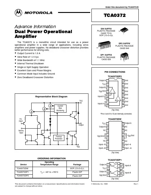
TCA305资料
- 格式:pdf
- 大小:116.59 KB
- 文档页数:7
Semiconductor Group1 TCA 305
TCA 355 TCA 305TCA 355
Bipolar IC
Features
qLower open-loop current consumption;I
S < 1 mA
qLower output saturation voltage
qThe temperature dependence of the switching
distance is lower and compensation of the resonant
circuitTC (temperature coefficient) is easier
qThe sensitivity is higher, so that larger switching
distances are possible and coils of a lower quality can
be used
qThe switching hysteresis remains constant as regards
temperature, supply voltage and switching distance
qThe TCA 305 even functions without external
integrating capacitor. With an external capacitor (or
with RC combination) good noise immunity can be
achieved
qThe outputs are temporarily short-circuit proof (approx.
10 s to 1 min depending on package)
qThe outputs are disabled whenV
S < approx. 4.5 V and
are enabled when the oscillator stabilizes
(fromV
S min = 5 V)
qHigher switching frequencies can be obtained
qMiniature packageProximity Switch
P-DSO-8-1
P-DIP-14-1
P-DSO-14-1
TypeOrdering Code
TCA 305 AQ67000-A2291Package
P-DIP-14-1
TCA 305 GQ67000-A2305P-DSO-14-1 (SMD)
TCA 355 GQ67000-A2444P-DSO-8-1 (SMD)s
sNot for new design
01.96元器件交易网www.cecb2b.com
Semiconductor Group
2 TCA 305
TCA 355
TCA 305 A
TCA 305 G
The devices TCA 305 and TCA 355 contain all the functions necessary to design inductive
proximity switches. By approaching a standard metal plate to the coil, the resonant circuit is
damped and the outputs are switched.
Operation Schematic: see TCA 205
The types TCA 305 and TCA 355 have been developed from the type TCA 205 and are out-
standing for the following characteristics:
Logic Functions
OscillatorOutputs
Q
not damped
dampedH
LL
HTCA 355 G
Pin Configurations(top view)元器件交易网www.cecb2b.com
Semiconductor Group
3 TCA 305
TCA 355
Block Diagram
Standard Turn-ON Delay Referred toT
A
= 25 ˚C元器件交易网www.cecb2b.com
Semiconductor Group
4 TCA 305
TCA 355Absolute Maximum Ratings
Operating Range
Characteristics
V
S = 12 V,T
A = – 25 to 85 ˚CParameterSymbolUnitLimit Values
Supply voltage
Output voltageV
S
V
Q35
35
Output currentI
QmA50V
V
Junction temperature
Storage temperature rangeT
j
T
stg150
– 55 to 125˚C
˚C
Thermal resistance
system - airTCA 305 A
TCA 305 GR
th SA
R
th SA85 (135)2)
140 (200)2)K/W
K/WDistance, hysteresis resistanceR
Di,R
HyΩ0
CapacitancesC
I,C
DµF5
Supply voltageV
SV5 to 303)
Oscillator frequencyf
OSCMHz0.015 to 1.5
Ambient temperatureT
A˚C– 25 to 85
Parameter
typ.min.max.UnitTest
ConditionLimit ValuesSymbol
Open-loop
current consumption0.60.9
(1.0)2)mAoutputs openI
S
Reference voltage1)
L-output voltage
per output3.2
0.04
0.10
0.220.15
0.35
0.75V
V
V
VI
REF< 10
µA
I
Q L = 5 mA
I
Q L = 25 mA
I
Q L = 50 mAV
REF
V
Q L
V
Q L
V
Q L
H-output current per output10
µAV
Q H = 30 VI
Q H
Threshold at 3
Hysteresis at 32.1
0.50.40.6V
VV
S 3
V
Hy
Turn-ON delay1)600– 25 %– 25 %ms/
µFT
A = 25 ˚Ct
D ON
Switching frequency w/o C
I5kHzf
S
1)TCA 305 only
2)Values in parenthesis apply to TCA 355 only
3)Operation at voltages less than 5 V (between approx. 2.5 and 5 V) is possible, ifV
REF is connected toV
S. In
this caseV
REF is no longer internally stabilized. Additionally, the pin "turn-on delay" is to be applied as follows:
If no turn-on delay is needed, this pin has to be connected toV
S. If, however, a turn-on delay is required, the
charge current forD
D has to be adjusted with an external resistor between this pin andV
S (recommended
value 390 k).Ω元器件交易网www.cecb2b.com
Semiconductor Group
5 TCA 305
TCA 355
Schematic Circuit Diagram
OscilatorTurn-ON Delay for TCA 305 A; G
Integrating CapacitorOutputs元器件交易网www.cecb2b.com
Semiconductor Group
6 TCA 305
TCA 355
Application Circuit元器件交易网www.cecb2b.com
Semiconductor Group
7 TCA 305
TCA 355
L
0,C
0Resonant circuit
R
HyHysteresis adjustment
R
DiDistance adjustment
DTemperature compensation of the resonant circuit; possibly with series
resistance for the purpose of adjustment. The diode is not absolutely necessary.
Whether it is used or not depends on the temperature coefficient of the resonant
circuit.
R
I;C
IIntegration element. At pin 3 (integrating capacitance) we recommend a
capacitor of typ. 1 nF. To increase noise immunity this capacitor can be
substituted by an RC circuit with, e.g.,R
I = 1 M andC
I = 10 nF.
C
DDelay capacitor
Dimensioning Examples in Accordance with CENELEC Standard (flush)Ω
M 12M 18M 30
Ferrite pot core
Number of turns
Cross section of wire
L
0
C
0 (STYROFLEX®)
f
OSC
Sn
R
A (Metal)
C
DM 33 (7.35
×3.6) mm
100
0.1 CuL
206
µH
1000 pF
appr. 350 kHz
4 mm
8.2 k + 330
100 nFΩΩN 22 (14.4
× 7.5) mm
80
20
× 0.05
268
µH
1.2 nF
appr. 280 kHz
8 mm
33 k
100 nFΩN 22 (25
× 8.9) mm
100
10
× 0.1
585
µH
3.3 nF
appr. 115 kHz
15 mm
22 k + 2.7 k
100 nFΩΩ元器件交易网www.cecb2b.com