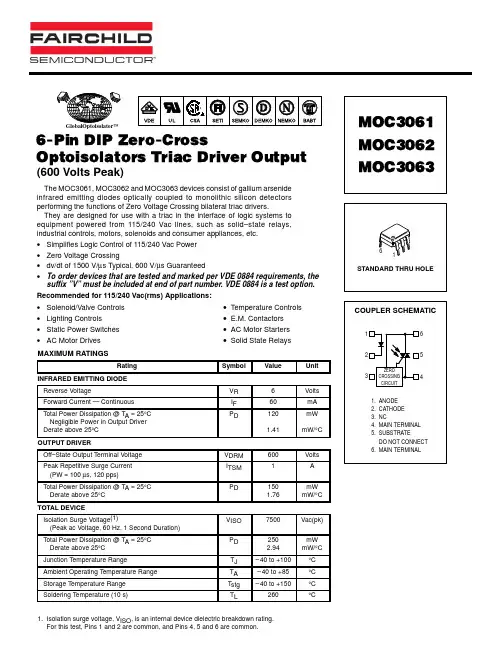
TD3063资料
- 格式:pdf
- 大小:481.11 KB
- 文档页数:5
TD3063
Zero-Volt SwitchingTriac Driver
The TD3063 consists of a single input LED optically coupled to a zero-volt crossing triac driver. The TD3063 provides high input-to-output isolation and is designed to drive high-powered triacs. Typical uses include interfacing logic level control signals to equipment powered from 110Vac and 220Vac lines.DESCRIPTION
FEATURESAPPLICATIONS
OPTIONS/SUFFIXES*
SCHEMATIC DIAGRAMABSOLUTE MAXIMUM RATINGS*APPROVALSZero-volt switching•
600V blocking voltage•
High input-to-output isolation (5kV)•
Low trigger current (5mA MAX)•
High reliability• Home appliances•
Motor/ Drive controls•
Solid state relays•
Solenoid / Valve control•
Temperature Control•
Surface Mount Leadform Option• -S
Tape and Reel Option• -TR
Signifies VDE approval• -V
0.4" Lead Spacing (see mechanical dimension)• -H
NOTE: Suffixes listed above are not included in marking on device for part number identification.PARAMETERUNITMINTYPMAX
Storage Temperature°C-55125
Operating Temperature°C-4085
Continuous Input CurrentmA50
Transient Input CurrentmA400
Reverse Input Control VoltageV6
Total Power DissipationmW330
Soldering Temperature (10s)ºC260
*The values indicated are absolute stress ratings. Functional operation of the device is not implied at these or any conditions in excess of those defined in electrical characteristics section of this document. Exposure to Absolute Ratings may cause permanent damage to the device and may adversely affect reliability. 1
2 + Input
- Input
3 6
5
4 +/- AC Output
Do Not Use
-/+ AC Output
UL and C-UL Approved File # E201932•
VDE Approved, Lic # 40011225•
© 2004 Solid State Optronics • San José, CA
www.ssousa.com • +1.408.293.4600Page 1 of 5TD3063
rev 1.40 (10/25/2004)TD3063
Zero-Volt SwitchingTriac Driver ELECTRICAL CHARACTERISTICS - 25°CPARAMETERUNITMINTYPMAX TEST CONDITIONS
INPUT SPECIFICATIONS
LED Forward VoltageV1.21.5If = 10mA
LED Reverse VoltageV612Ir = 10uA
Reverse Leakage Currentµ10Vr = 4VA
OUTPUT SPECIFICATIONS
Blocking VoltageV600Io = 1uA
Peak Blocking Currentn60500Vdrm = RatedA
On-state VoltageV1.83Itm = 100mA
Critical Rate of RiseV600/µs
COUPLED SPECIFICATIONS
Isolation VoltageV5000T = 1 minute
Trigger Currentm5Main terminal voltage = 3VA
Inhibit VoltageV520If = 5mA
Isolation ResistanceG50DC 500VΩ
Holding Currentµ100A
Leakage Currentµ1If = Rated, Vdrm = Rated, Off StateA
© 2004 Solid State Optronics • San José, CA
www.ssousa.com • +1.408.293.4600Page 2 of 5TD3063
rev 1.40 (10/25/2004)TD3063
Zero-Volt SwitchingTriac Driver PERFORMANCE DATA
© 2004 Solid State Optronics • San José, CA
www.ssousa.com • +1.408.293.4600Page 3 of 5TD3063
rev 1.40 (10/25/2004)Fig.2Inhibit Voltage versusTemperature
Ta,AMBIENT TEMPERATURE (°C)VINH, NORMALIZEDFig.1On-State Characteristics
VTM,ON-STATE VOLTAGE (VOLTS)ITM,ON-STATE CURRENT (mA)Fig.3Leakage with LED Off versusTemperature
Ta,AMBIENT TEMPERATURE (°C)IDRM1,PEAK BLOCKING CURRENT (nA)
Fig.5Trigger Current versusTemperature
Ta,AMBIENT TEMPERATURE (°C)IFT, NORMALIZEDFig.4IDRM2,Leakage in Inhibit Stateversus Temperature
Ta,AMBIENT TEMPERATURE (°C)IDRM2NORMALIZED
MECHANICAL DIMENSIONS
© 2004 Solid State Optronics • San José, CA
www.ssousa.com • +1.408.293.4600Page 4 of 5 TD3063
rev 1.40 (10/25/2004)6 PIN DUAL IN-LINE PACKAGE (Through Hole) 6 PIN SURFACE MOUNT DEVICE (SMD)
TOLERANCE :+ 0.25mmUnit in (mm)-H Suffix 0.4" Lead Spacing TD3063
Zero-Volt SwitchingTriac DriverTD3063
Zero-Volt SwitchingTriac Driver
Solid State Optronics (SSO) makes no warranties or representations with regards to the completeness and accuracy of this document. SSO reserves the right to make changes to product description, specifications at any time without further notice.SSO shall not assume any liability arising out of the application or use of any product or circuit described herein. Neither circuit patentlicenses nor indemnity are expressed or implied.Except as specified in SSO's Standard Terms & Conditions, SSO disclaims liability for consequential or other damage, and we make no otherwarranty, expressed or implied, including merchantability and fitness for particular use.DISCLAIMER
LIFE SUPPORT POLICY
SSO does not authorize use of its devices in life support applications wherein failure or malfunction of a device may lead to personal injury ordeath. Users of SSO devices in life support applications assume all risks of such use and agree to indemnify SSO against any and alldamages resulting from such use. Life support devices are defined as devices or systems which, (a) are intended for surgical implant into thebody, or (b) support or sustain life, and (c) whose failure to perform when used properly in accordance with instructions for use can bereasonably expected to result in significant injury to the user, or (d) a critical component in any component of a life support device or systemwhose failure can be reasonably expected to cause failure of the life support device or system, or to affect its safety or effectiveness.