倒装芯片技术课件
- 格式:ppt
- 大小:8.87 MB
- 文档页数:10
摘要:倒装芯片在产品成本,性能及满足高密度封装等方面体现出优势,它的应用也渐渐成为主流。
由于倒装芯片的尺寸小,要保证高精度高产量高重复性,这给我们传统的设备及工艺带来了挑战。
器件的小型化高密度封装形式越来越多,如多模块封装(MCM )、系统封装(SiP )、倒装芯片(FC ,Flip-Chip )等应用得越来越多。
这些技术的出现更加模糊了一级封装与二级装配之间的界线。
毋庸置疑,随着小型化高密度封装的出现,对高速与高精度装配的要求变得更加关键,相关的组装设备和工艺也更具先进性与高灵活性。
由于倒装芯片比BGA 或CSP 具有更小的外形尺寸、更小的球径和球间距、它对植球工艺、基板技术、材料的兼容性、制造工艺,以及检查设备和方法提出了前所未有的挑战。
倒装芯片的发展历史倒装芯片的定义什么器件被称为倒装芯片?一般来说,这类器件具备以下特点:1. 基材是硅;2. 电气面及焊凸在器件下表面;3. 球间距一般为4-14mil 、球径为2.5-8mil 、外形尺寸为1 -27mm ;4. 组装在基板上后需要做底部填充。
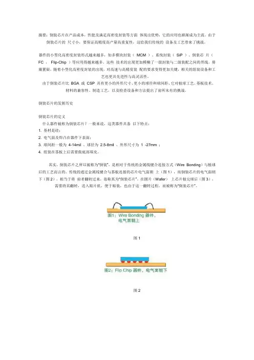
其实,倒装芯片之所以被称为“倒装”,是相对于传统的金属线键合连接方式(Wire Bonding)与植球后的工艺而言的。
传统的通过金属线键合与基板连接的芯片电气面朝上(图1),而倒装芯片的电气面朝下(图2),相当于将前者翻转过来,故称其为“倒装芯片”。
在圆片(Wafer)上芯片植完球后(图3),需要将其翻转,送入贴片机,便于贴装,也由于这一翻转过程,而被称为“倒装芯片”。
图1图2图3倒装芯片的历史及其应用倒装芯片在1964年开始出现,1969年由IBM发明了倒装芯片的C4工艺(Controlled Collap se Chip Connection,可控坍塌芯片联接)。
过去只是比较少量的特殊应用,近几年倒装芯片已经成为高性能封装的互连方法,它的应用得到比较广泛快速的发展。
目前倒装芯片主要应用在Wi- Fi、SiP、M CM、图像传感器、微处理器、硬盘驱动器、医用传感器,以及RFID等方面(图5)。
led倒装芯片封装技术英文回答:## Flip Chip LED Packaging Technology.Flip chip LED packaging technology is a method of mounting LED chips on a printed circuit board (PCB) with the active side of the chip facing down. This technology offers several advantages over traditional surface mount technology (SMT), including:Reduced package height: Flip chip LEDs are much thinner than SMT LEDs, allowing for the creation of thinner and more compact lighting fixtures.Improved thermal performance: The direct thermal contact between the LED chip and the PCB dissipates heat more efficiently, resulting in longer LED life and improved performance.Higher power density: Flip chip LEDs can be packed more densely than SMT LEDs, enabling the creation of high-power lighting fixtures with a smaller footprint.Lower cost: Flip chip LEDs are less expensive to manufacture than SMT LEDs, making them a more cost-effective option for large-scale lighting applications.Flip chip LED packaging technology is typically used in applications where high power density and thermal performance are critical, such as automotive lighting, street lighting, and commercial lighting.### Flip Chip LED Packaging Process.The flip chip LED packaging process involves the following steps:1. Die preparation: The LED chip is prepared by thinning the substrate and applying a solder mask to the active surface.2. Solder ball attachment: Solder balls are attached to the bottom surface of the LED chip using a solder paste.3. Chip placement: The LED chip is placed on the PCB with the solder balls facing down.4. Reflow soldering: The PCB is heated to melt the solder balls and form a permanent connection between the LED chip and the PCB.5. Encapsulation: The LED chip is encapsulated with a protective epoxy to protect it from the environment.### Advantages of Flip Chip LED Packaging Technology.The advantages of flip chip LED packaging technology include:Reduced package height: Flip chip LEDs are muchthinner than SMT LEDs, allowing for the creation of thinner and more compact lighting fixtures.Improved thermal performance: The direct thermal contact between the LED chip and the PCB dissipates heat more efficiently, resulting in longer LED life and improved performance.Higher power density: Flip chip LEDs can be packedmore densely than SMT LEDs, enabling the creation of high-power lighting fixtures with a smaller footprint.Lower cost: Flip chip LEDs are less expensive to manufacture than SMT LEDs, making them a more cost-effective option for large-scale lighting applications.### Disadvantages of Flip Chip LED Packaging Technology.The disadvantages of flip chip LED packaging technology include:Higher assembly cost: The flip chip LED packaging process is more complex than the SMT process, resulting in higher assembly costs.Limited design flexibility: The rigid nature of the flip chip LED package limits design flexibility, making it difficult to create custom lighting fixtures.Reliability concerns: The flip chip LED package is more susceptible to mechanical stress than the SMT package, raising reliability concerns for applications where vibration or shock is a factor.### Conclusion.Flip chip LED packaging technology offers several advantages over traditional SMT, including reduced package height, improved thermal performance, higher power density, and lower cost. However, this technology also has some disadvantages, including higher assembly cost, limited design flexibility, and reliability concerns. Overall, flip chip LED packaging technology is a valuable option for applications where high power density and thermal performance are critical.中文回答:## 倒装芯片LED封装技术。
倒装芯片键合技术
嘿,朋友们!今天咱来聊聊这个倒装芯片键合技术呀!这玩意儿可神奇了,就像是给电子世界搭起了一座特别的桥梁。
你想想看,那些小小的芯片,就好像是一个个小精灵,它们有着巨大的能量和潜力。
而倒装芯片键合技术呢,就是让这些小精灵能够稳稳地待在它们该在的地方,发挥出它们的本领。
它就像是一个超级厉害的魔术师,能把芯片和基板紧紧地连在一起,让它们亲密无间地合作。
这可不是随随便便就能做到的呀!这需要非常精细的操作和高超的技艺。
比如说吧,就好像我们盖房子,得把每一块砖都放得稳稳当当的,这样房子才不会摇摇晃晃。
倒装芯片键合技术也是这样,要把芯片准确无误地键合到基板上,稍有偏差都不行呢!这可真是个技术活啊!
而且啊,这个技术还在不断发展和进步呢!就像我们人一样,要不断学习和成长。
它变得越来越厉害,能让我们的电子设备越来越小巧、越来越强大。
你再想想,要是没有这个倒装芯片键合技术,我们的手机能这么智能吗?我们的电脑能这么快速吗?那肯定不行呀!它就像是背后的无名英雄,默默地为我们的科技生活贡献着力量。
你说,这倒装芯片键合技术是不是很了不起?它让那些小小的芯片发挥出了大大的作用,让我们的生活变得更加丰富多彩。
我们真应该好好感谢这个神奇的技术呀!它就像是给我们的科技世界注入了一股强大的动力,推动着我们不断向前。
所以呀,可别小瞧了它哟!这就是倒装芯片键合技术,一个充满魅力和神奇的技术!。
倒装cob封装工艺
倒装COB封装工艺是一种先进的集成电路封装技术,COB是
Chip on Board的缩写,意为芯片直接封装在基板上。
倒装COB封
装工艺相比传统封装技术具有一些优势。
首先,倒装COB封装工艺可以有效减小封装尺寸,提高集成度。
由于芯片直接封装在基板上,不需要额外的封装材料和封装空间,
因此可以实现更小型化的封装,适用于轻薄化、小型化的电子产品
设计。
其次,倒装COB封装工艺可以提高散热性能。
由于芯片直接与
基板接触,热量可以更快更有效地传导到基板上,利于散热,有利
于提高芯片的工作稳定性和可靠性。
此外,倒装COB封装工艺可以降低封装成本。
相比传统封装技术,倒装COB封装省去了一些封装材料和工序,可以降低生产成本,提高生产效率。
然而,倒装COB封装工艺也存在一些挑战和局限性。
例如,对
基板的要求较高,需要优质的基板材料和制造工艺;另外,倒装
COB封装需要特殊的焊接工艺,对生产工艺要求较高。
总的来说,倒装COB封装工艺在一定的应用场景下具有明显的优势,但也需要克服一些技术难题。
随着技术的不断进步和应用需求的不断变化,倒装COB封装工艺有望在未来得到更广泛的应用和发展。
倒装芯片:向主流制造工艺推进时间:2009-12-08来源:责任编辑:对较小外形和较多功能的低成本电子设备的需求继续在增长。
这些快速调整的市场挑战着电子制造商,降低制造成本以保证可接受的利润率。
倒装芯片装配(flip chip assembly)被认为是推进低成本、高密度便携式电子设备的制造所必须的一项技术。
在低成本应用中,倒装芯片的成功是因为它可达到相对于传统表面贴装元件包装更大的成本效益。
例如,一款新的寻呼机利用了倒装芯片技术将微控制器装配于PCB,因为倒装芯片使用较少的电路板空间,比传统的塑料球栅阵列(PBGA, plastic ball grid array)成本较低。
材料集成电路(Integraded circuit)在这款寻呼机中的集成电路(IC, integrated circuit)是一个5 x 5.6 mm 的微控制器,要求100个输入/输出(I/O)连接于PCB。
将四周I/O重新分配为2.5排减少点数(depopulated)的球栅阵列形式来接纳PCB的线/空格以及通路孔焊盘的限制。
锡球(bump)布局与间距如图一所示。
使用了电镀共晶锡/铅锡球,因为与其它的替代者比較,它的成本低得多。
锡球的直径大约为125 %26mu;m,球下金属(UBM, under bump metalization)为一个顾客要求的45%26mu;m的铜柱,如图二。
印刷电路板(PCB, printed circuit board)成本因素决定这款寻呼机的PCB的布局。
PCB是标准的FR-4,四个金属层和一个无电镀镍/金表面涂层。
因为增加材料成本和有限的可获得性,所以没有使用高密度互连(HDI, high-density interconnect)技术。
无电镀镍/金表面涂层满足所有作品的要求。
实录可靠性问题排除了选择有机可焊性保护层(OSP, organic solderability preservative),选择性镍-金的成本增加也没有吸引性。
倒装芯片封装工艺倒装芯片封装工艺,这可是个厉害的家伙!你知道吗,它就像是给芯片穿上了一层超级酷炫的“防护服”。
先来说说倒装芯片到底是啥。
这就好比是一个小巧玲珑但又超级重要的“大脑”,里面藏着无数的秘密和智慧。
而封装工艺呢,就是要把这个“大脑”好好保护起来,让它能稳定工作,不受外界的干扰和伤害。
倒装芯片封装的第一步,得先把芯片准备好,就像运动员要上场比赛,得先热身,调整到最佳状态。
这芯片也一样,得保证它没有任何瑕疵和毛病。
然后呢,在基板上涂上一层神奇的胶水,这胶水可厉害了,能把芯片牢牢粘住。
这就好像给芯片安了个舒服的“家”。
接下来,就是把芯片倒扣在基板上,这动作是不是有点像我们平时翻个跟头?可别小看这一倒,这可是整个工艺的关键步骤,得小心翼翼,不能有半点差错。
倒装完成后,就得进行连线了。
这连线就像是给芯片修了一条条高速公路,让信息能快速、畅通无阻地传递。
这线得多细多精密啊,简直比头发丝还细!要是稍微出点差错,那可就糟糕啦!再然后,就是封装材料的填充。
这就像是给芯片盖上了一层厚厚的被子,保暖又安全。
这材料得选好,不能让芯片觉得“冷”或者“闷”。
最后,还得进行各种测试,看看封装好的芯片是不是真的厉害。
这就像是考试,得检验一下之前的努力有没有成果。
你想想,如果没有这倒装芯片封装工艺,我们的手机能那么智能吗?电脑能运行得那么快吗?各种高科技设备能给我们带来那么多便利吗?所以说啊,这倒装芯片封装工艺虽然听起来复杂,但是它的作用可大了去啦!总之,倒装芯片封装工艺就是高科技领域里的一位超级英雄,默默地守护着芯片,让我们的生活变得更加美好!。