PL1167中文资料-2.4GHz无线射频收发芯片讲解
- 格式:doc
- 大小:834.51 KB
- 文档页数:12
EFR32xG24 2.4 GHz 10 dBm Radio Board BRD4186C Reference ManualThe BRD4186C Radio Board is an excellent starting point to get familiar with theEFR32™ Wireless Gecko Wireless System-on-Chip. The board enables developers to develop smart home, lighting, building automation, and AI/ML applications. It is opti-mized for operating in the 2.4 GHz band at 10 dBm output power. Radiated and conduc-ted testing is supported with the on-board printed antenna and UFL connector.The BRD4186C Radio Board is a plug-in board for the Wireless Starter Kit Mainboard (BRD4001A) and the Wireless Gecko Pro Kit Mainboard (BRD4002A) that gives access to debug interface, Virtual COM port, packet trace, display, buttons, LEDs, and addition-al features from expansion boards. With the supporting Simplicity Studio suite of tools, developers can take advantage of graphical wireless application development and visu-al energy profiling and optimization. The board also serves as a reference design for the EFR32xG24 Wireless SoC with matching network and a PCB antenna optimized for op-erating at 10 dBm output power in the 2.4 GHz band.RADIO BOARD FEATURES •Wireless SoC:EFR32MG24B210F1536IM48•CPU core: ARM® Cortex®-M33•Flash memory: 1536 kB•RAM: 256 kB•Operation frequency: 2.4 GHz•Transmit power: 10 dBm•Integrated PCB antenna, UFL connector(optional)•Crystals for LFXO and HFXO: 32.768 kHzand 39 MHz•8 Mbit low-power serial flash for over-the-air updatesThis document contains a brief introduction and description of the BRD4186C RadioBoard features, focusing on the RF sections and performance.Table of Contents1. Introduction (4)2. Radio Board Connector (5)2.1 Introduction (5)2.2 Radio Board Connector Pin Associations (5)3. Radio Board Block Summary (6)3.1 Introduction (6)3.2 Radio Board Block Diagram (6)3.3 Radio Board Block Description (6)3.3.1 Wireless MCU (6)3.3.2 LF Crystal Oscillator (LFXO) (6)3.3.3 HF Crystal Oscillator (HFXO) (6)3.3.4 Matching Network for 2.4 GHz (7)3.3.5 UFL Connector (7)3.3.6 Radio Board Connectors (7)3.3.7 Inverted-F Antenna (7)3.3.8 Serial Flash (7)3.3.9 Serial EEPROM (7)4. RF Section (8)4.1 Introduction (8)4.2 RF Section Schematic (8)4.2.1 2.4 GHz RF Matching Description (8)4.3 Bill of Materials for the 2.4 GHz Matching Network (8)4.4 Inverted-F Antenna (9)5. Mechanical Details (10)6. EMC Compliance (11)6.1 Introduction (11)6.2 EMC Regulations for 2.4 GHz (11)6.2.1 ETSI EN 300-328 Emission Limits for the 2400-2483.5 MHz Band (11)6.2.2 FCC15.247 Emission Limits for the 2400-2483.5 MHz Band (11)6.2.3 Applied Emission Limits for the 2.4 GHz Band (11)7. RF Performance (12)7.1 Conducted Power Measurements (12)7.1.1 Conducted Power Measurements with Unmodulated Carrier (12)7.1.2 Conducted Power Measurements with Modulated Carrier (13)7.2 Radiated Power Measurements (13)7.2.1 Maximum Radiated Power Measurements (14)7.2.2 Antenna Pattern Measurements (14)8. EMC Compliance Recommendations (15)8.1 Recommendations for 2.4 GHz ETSI EN 300-328 Compliance (15)8.2 Recommendations for 2.4 GHz FCC 15.247 Compliance (15)9. Board Revision History (16)10. Errata (17)11. Document Revision History (18)Introduction 1. IntroductionThe BRD4186C Radio Boards provide a development platform (together with the Wireless Starter Kit Mainboard or the Wireless Pro Kit Mainboard) for the Silicon Labs EFR32MG24 Wireless System-on-Chips and serve as reference designs for the matching network of the RF interface.The BRD4186C Radio Board is designed to operate in the 2400-2483.5 MHz band with the RF matching network optimized for operat-ing at 10 dBm output power.To develop and/or evaluate the EFR32 Wireless Gecko, the BRD4186C Radio Board can be connected to the Wireless Starter Kit Mainboard or the Wireless Pro Kit Mainboard to get access to debug interface, Virtual COM port, packet trace, display, buttons, LEDs, and additional features from expansion boards, and also to evaluate the performance of the RF interface.2. Radio Board Connector2.1 IntroductionThe board-to-board connector scheme allows access to all EFR32MG24 GPIO pins as well as the RESETn signal. For more informa-tion on the functions of the available pins, see the EFR32MG24 data sheet.2.2 Radio Board Connector Pin AssociationsThe figure below shows the mapping between the connector and the EFR32MG24 pins and their function on the Wireless Starter Kit Mainboard.GND F9 / PA00 / VCOM_RTS 3v3JOYSTICK* / PD02* / P36P200Upper RowNC / P38NC / P40DBG_TDO_SWO / TRACED0 / PA03 / P42TRACED2 / PA06 / P44DBG_TMS_SWDIO / PA02 / F0DISP_ENABLE / PC09 / F14UIF_BUTTON0 / PB01 / F12UIF_LED0 / PB02 / F10VCOM_CTS / PB05 / F8DBG_RESET / RESETn / F4DBG_TDO_SWO / TRACED0 / PA03 / F2DISP_SI / PC01 / F16VCOM_TX / PA08 / F6PTI_DATA / PD04 / F20DISP_EXTCOMIN / PC06 / F18USB_VBUS5VBoard ID SCLGNDBoard ID SDAUSB_VREG F7 / PA09 / VCOM_RX F5 / PB00 / VCOM_ENABLE F3 / PA04 / DBG_TDI / TRACECLK F1 / PA01 / DBG_TCK_SWCLK P45 / PA07 / TRACED3P43 / PA05 / TRACED1P41 / PA04 / DBG_TDI / TRACECLK P39 / NCP37 / NC F11 / PB04 / UIF_LED1F13 / PB03 / UIF_BUTTON1F15 / PC03 / DISP_SCLK F17 / PC08 / DISP_SCS F19 / PD05 / PTI_SYNC F21 / NC GNDVMCU_INVCOM_CTS / PB05 / P0P201Lower RowVCOM_RTS / PA00 / P2TRACED1 / PA05 / P4JOYSTICK* / PD02* / P6GNDVRF_INP35 / PC04P7 / PC00P5 / PC03 / DISP_SCLK P3 / PC02P1 / PC01 / DISP_SI P33 / PC06 / DISP_EXTCOMIN P31 / PC08 / DISP_SCSP29 / PC09 / DISP_ENABLE P27 / NCP25 / PD04 / PTI_DATA P23 / NCP21 / PB03 / UIF_BUTTON1P19 / PB02 / UIF_LED0P17 / PB01 / UIF_BUTTON0P15 / PB00 / VCOM_ENABLE P13 / PC07P11 / PA09 / VCOM_RX P9 / PA08 / VCOM_TX NC / P34NC / P32NC / P30NC / P28UIF_LED1 / PB04 / P26PTI_SYNC / PD05 / P24NC / P22DBG_TCK_SWCLK / PA01 / P20DBG_TMS_SWDIO / PA02 / P18DBG_TDO_SWO / TRACED0 / PA03 / P16DBG_TDI / TRACECLK / PA04 / P14PC05 / P12TRACED3 / PA07 / P10TRACED2 / PA06 / P8 *Mutually exclusive connections. Default: PD02 to P6.Figure 2.1. BRD4186C Radio Board Connector Pin MappingRadio Board Connector3. Radio Board Block Summary3.1 IntroductionThis section introduces the blocks of the BRD4186C Radio Board.3.2 Radio Board Block DiagramThe block diagram of the BRD4186C Radio Board is shown in the figure below.Figure 3.1. BRD4186C Block Diagram3.3 Radio Board Block Description3.3.1 Wireless MCUThe BRD4186C Radio Board incorporates an EFR32MG24B210F1536IM48 Wireless System-on-Chip featuring 32-bit Cortex®-M33 core, 1536 kB of flash memory, 256 kB of RAM, and a 2.4 GHz band transceiver with output power up to 10 dBm. For additional infor-mation on the EFR32MG24B210F1536IM48, refer to the EFR32MG24 data sheet.3.3.2 LF Crystal Oscillator (LFXO)The BRD4186C Radio Board has a 32.768 kHz crystal mounted. For details regarding the crystal configuration, refer to application note AN0016.2: Oscillator Design Considerations.3.3.3 HF Crystal Oscillator (HFXO)The BRD4186C Radio Board has a 39 MHz crystal mounted. For details regarding the crystal configuration, refer to application note AN0016.2: Oscillator Design Considerations.3.3.4 Matching Network for 2.4 GHzThe BRD4186C Radio Board incorporates a 2.4 GHz matching network which connects the 2.4 GHz RF input/output of the EFR32MG24 to the one on-board printed Inverted-F antenna. The component values were optimized for the 2.4 GHz band RF perform-ance and current consumption with 10 dBm output power.For a detailed description of the matching network, see section 4.2.1 2.4 GHz RF Matching Description.3.3.5 UFL ConnectorTo be able to perform conducted measurements, Silicon Labs added a UFL connector to the Radio Board. The connector allows an external 50 Ohm cable or antenna to be connected during design verification or testing.Note: By default, the output of the matching network is connected to the printed inverted-F antenna by a series 0 Ohm resistor. To support conducted measurements, or the connection of an external antenna, the option to connect the output to the UFL connector is available. If using this option, move the series 0 Ohm resistor to the antenna to the series resistor to the UFL connector (see section 4.2.1 2.4 GHz RF Matching Description for further details). On the layout, the footprints of these two resistors have overlapping pads to prevent simultaneous connection of the antenna and the UFL connector.3.3.6 Radio Board ConnectorsTwo dual-row, 0.05” pitch polarized connectors make up the BRD4186C Radio Board interface to the Wireless Starter Kit Mainboard. For more information on the pin mapping between the EFR32MG24B210F1536IM48 and the connectors, refer to section 2.2 Radio Board Connector Pin Associations.3.3.7 Inverted-F AntennaThe BRD4186C Radio Board includes a printed inverted-F antenna (IFA) tuned to have close to 50 Ohm impedance at the 2.4 GHz band.For a detailed description of the antenna, see section 4.4 Inverted-F Antenna.3.3.8 Serial FlashThe BRD4186C Radio Board is equipped with an 8 Mbit Macronix MX25R SPI flash that is connected directly to the EFR32MG24 to support over-the-air (OTA) updates. For additional information on the pin mapping, see the BRD4186C schematic.3.3.9 Serial EEPROMThe BRD4186C Radio Board is equipped with a serial I2C EEPROM for board identification and to store additional board-related infor-mation.4. RF Section4.1 IntroductionThis section gives a short introduction to the RF section of the BRD4186C Radio Board.4.2 RF Section SchematicBRD4186C Radio Board RF section schematic is shown in the following figure.2.4 GHz Matching Path SelectionInverted-F AntennaAntenna Tuning High Frequency Figure 4.1. BRD4186C RF Section Schematic4.2.1 2.4 GHz RF Matching DescriptionThe 2.4 GHz RF matching connects the 2G4RF1 pin to the on-board printed IFA. The component values were optimized for the 2.4 GHz band RF performance and current consumption with the targeted 10 dBm output power.The matching network consists of a five-element impedance matching and harmonic filter circuitry and a DC blocking capacitor (not required for the 20 dBm part).For conducted measurements, the matching network output can also be connected to the UFL connector by removing the series R1resistor (0 Ohm) between the antenna and the matching network and mounting it to the R2 resistor position between the matching net-work and the UFL connector.4.3 Bill of Materials for the 2.4 GHz Matching NetworkThe bill of materials for the BRD4186C Radio Board 2.4 GHz matching network is shown in the following table.Table 4.1. Bill of Materials for the BRD4186C 2.4 GHz RF Matching Network4.4 Inverted-F AntennaThe BRD4186C Radio Board includes an on-board, printed inverted-F antenna, tuned for the 2.4 GHz band. Due to the design restric-tions of the radio board, the input of the antenna and the output of the matching network can't be placed directly next to each other. Therefore, a 50 Ohm transmission line was necessary to connect them.The resulting impedance that is presented to the matching network output is shown in the following figure. During the measurement, the BRD4186C Radio Board was attached to a Wireless Starter Kit Mainboard.As shown in the figure, the antenna impedace (blue curve) is close to 50 Ohm in the entire 2.4 GHz band, and the reflection (red curve) is under -10 dB.Figure 4.2. Impedance and Reflection of the Inverted-F Antenna of the BRD4186C Board Measured from the Matching Output5. Mechanical DetailsThe BRD4186C Radio Board is illustrated in the figures below.45 mm30 mmFigure 5.1. BRD4186C Top View24 mm5 mm Interface ConnectorInterface ConnectorFigure 5.2. BRD4186C Bottom ViewMechanical DetailsEMC Compliance 6. EMC Compliance6.1 IntroductionBRD4186C Radio Board fundamental and harmonic levels compliance is tested against the following standards:• 2.4 GHz:•ETSI EN 300-328•FCC 15.2476.2 EMC Regulations for 2.4 GHz6.2.1 ETSI EN 300-328 Emission Limits for the 2400-2483.5 MHz BandBased on ETSI EN 300-328, the allowed maximum fundamental power for the 2400-2483.5 MHz band is 20 dBm EIRP. For the unwan-ted emissions in the 1 GHz to 12.75 GHz domain, the specific limit is -30 dBm EIRP.6.2.2 FCC15.247 Emission Limits for the 2400-2483.5 MHz BandFCC 15.247 allows conducted output power up to 1 W (30 dBm) in the 2400-2483.5 MHz band. For spurious emissions, the limit is -20 dBc based on either conducted or radiated measurement, if the emission is not in a restricted band. The restricted bands are speci-fied in FCC 15.205. In these bands, the spurious emission levels must meet the levels set out in FCC 15.209. In the range from 960 MHz to the frequency of the 5th harmonic, it is defined as 0.5 mV/m at 3 m distance, which equals to -41.2 dBm in EIRP.If operating in the 2400-2483.5 MHz band, the 2nd, 3rd, and 5th harmonics can fall into restricted bands. As a result, for those harmon-ics the -41.2 dBm limit should be applied. For the 4th harmonic, the -20 dBc limit should be applied.6.2.3 Applied Emission Limits for the 2.4 GHz BandThe above ETSI limits are applied both for conducted and radiated measurements.The FCC restricted band limits are radiated limits only. In addition, Silicon Labs applies the same restrictions to the conducted spec-trum. By doing so, compliance with the radiated limits can be estimated based on the conducted measurement by assuming the use of an antenna with 0 dB gain at the fundamental and the harmonic frequencies.The overall applied limits are shown in the table below. For the harmonics that fall into the FCC restricted bands, the FCC 15.209 limit is applied. ETSI EN 300-328 limit is applied for the rest.Table 6.1. Applied Limits for Spurious Emissions for the 2.4 GHz Band7. RF Performance7.1 Conducted Power MeasurementsDuring measurements, the BRD4186C Radio Board was attached to a Wireless Starter Kit Mainboard which was supplied by USB. The voltage supply for the radio board (VMCU) was 3.3 V and for the power amlifier (PAVDD), it was 1.8 V.7.1.1 Conducted Power Measurements with Unmodulated CarrierThe transceiver was operated in unmodulated carrier transmission mode. The output power of the radio was set to 10 dBm. The typical output spectrum is shown in the following figure.Figure 7.1. Typical Output Spectrum of the BRD4186C; PAVDD = 1.8 VAs shown in the figure, the fundamental is 10 dBm and all of the unwanted emissions are under the -41.2 dBm limit.Note: The conducted measurement is performed by connecting the on-board UFL connector to a spectrum analyzer through an SMA conversion adapter (P/N: HRMJ-U.FLP(40)). This connection itself introduces approximately 0.3 dB insertion loss.7.1.2 Conducted Power Measurements with Modulated CarrierDepending on the applied modulation scheme and the spectrum analyzer settings specified by the relevant EMC regulations, the meas-ured power levels are usually lower compared to the results with unmodulated carrier. These differences are measured and used as relaxation factors on the results of the radiated measurement performed with unmodulated carrier. This way, the radiated compliance with modulated transmission can be evaluated.In this case, both the ETSI EN 300-328 and the FCC 15.247 regulations define the following spectrum analyzer settings for measuring the unwanted emissions above 1 GHz:•Detector: Average•RBW: 1 MHzThe table below shows the measured differences for the supported modulation schemes.Table 7.1. Measured Relaxation Factors for the Supported Modulation SchemesAs shown, the BLE 125 Kb/s coded modulation scheme has the lowest relaxation factors. These values will be used as the worst case relaxarion factors for the radiated measurements.7.2 Radiated Power MeasurementsDuring measurements, the BRD4186C Radio Board was attached to a Wireless Starter Kit Mainboard which was supplied by USB. The voltage supply for the radio board was 3.3 V, for the power amlifier (PAVDD) it was 1.8 V. The radiated power was measured in an antenna chamber by rotating the board 360 degrees with horizontal and vertical reference antenna polarizations in the XY, XZ, and YZ cuts. The measurement planes are illustrated in the figure below.XZYFigure 7.2. Illustration of Reference Planes with a Radio BoardNote: The radiated measurement results presented in this document were recorded in an unlicensed antenna chamber. Also, the radi-ated power levels may change depending on the actual application (PCB size, used antenna, and so on). Therefore, the absolute levels and margins of the final application are recommended to be verified in a licensed EMC testhouse.7.2.1 Maximum Radiated Power MeasurementsFor the transmitter antenna, the on-board printed inverted-F antenna of the BRD4186C Radio Board was used (the R1 resistor was mounted). The supply for the RF section (RFVDD) and the 2.4 GHz power amplifier (PAVDD) was 1.8 V provided by the on-chip DC-DC converter; for details, see the BRD4186C schematic. The transceiver was operated in unmodulated carrier transmission mode. The output power of the radio was set to 10 dBm based on the conducted measurement.The results are shown in the tables below. The correction factors are applied based on the BLE 125 Kb/s coded modulation, shown in section 7.1.2 Conducted Power Measurements with Modulated Carrier . For the rest of the supported modulation schemes, the correction factors are larger, thus the related calculated margins would be higher compared to the ones shown in the table below. Thus,the margins below can be considered as worst case margins.Table 7.2. Maximums of the Measured Radiated Powers in EIRP [dBm] and the Calculated Modulated Margins in [dB] with theWireless Starter Kit Mainboard; PAVDD = 1.8 VAs shown in the table, with 10 dBm output power, the radiated power of the fundamental is higher than 10 dBm due to the high antenna gain. The 3rd harmonic is very close to the limit with the Wireless Starter Kit Mainboard in case of the unmodulated carrier transmis-sion. But with the relaxation of the supported modulation schemes, the margin is at least 5.1 dB.7.2.2 Antenna Pattern MeasurementsThe measured normalized antenna patterns are shown in the following figures.180°-35-30-25-20180°-35-30180°-35-30-25Figure 7.3. Normalized Antenna Pattern of the BRD4186C with the Wireless Starter Kit MainboardEMC Compliance Recommendations 8. EMC Compliance Recommendations8.1 Recommendations for 2.4 GHz ETSI EN 300-328 ComplianceAs shown in section 7.2 Radiated Power Measurements, the power of the BRD4186C fundamental with 10 dBm output is compliant with the 20 dBm limit of the ETSI EN 300-328 regulation. With the supported modulation schemes, the harmonics are also compliant with the relevant limits. Although the BRD4186C Radio Board has an option for mounting a shielding can, it is not required for compli-ance.8.2 Recommendations for 2.4 GHz FCC 15.247 ComplianceAs shown in section 7.2 Radiated Power Measurements, the power of the BRD4186C fundamental with 10 dBm output is compliant with the 30 dBm limit of the FCC 15.247 regulation. With the supported modulation schemes, the harmonics are also compliant with the relevant limits. Although the BRD4186C Radio Board has an option for mounting a shielding can, it is not required for compliance.9. Board Revision HistoryThe board revision is laser engraved in the Board Info field on the bottom side of the PCB, as outlined in the figure below. The revision printed on the silkscreen is the PCB revision.Board RevisionPCB RevisionBRD4186C Rev. A01P C B 4186C R e v . A 01184500348Figure 9.1. Revision InfoTable 9.1. BRD4186C Radio Board Revision HistoryBoard Revision HistoryErrata 10. ErrataThere are no known errata at present.Document Revision History 11. Document Revision HistoryRevision 1.0April, 2022•Initial document release.IoT Portfolio/IoTSW/HW/simplicityQuality/qualitySupport & Community/communitySilicon Laboratories Inc.400 West Cesar Chavez Austin, TX 78701USADisclaimerSilicon Labs intends to provide customers with the latest, accurate, and in-depth documentation of all peripherals and modules available for system and software implementers using or intending to use the Silicon Labs products. Characterization data, available modules and peripherals, memory sizes and memory addresses refer to each specific device, and “Typical” parameters provided can and do vary in different applications. Application examples described herein are for illustrative purposes only. Silicon Labs reserves the right to make changes without further notice to the product information, specifications, and descriptions herein, and does not give warranties as to the accuracy or completeness of the included information. Without prior notification, Silicon Labs may update product firmware during the manufacturing process for security or reliability reasons. Such changes will not alter the specifications or the performance of the product. Silicon Labs shall have no liability for the consequences of use of the information supplied in this document. This document does not imply or expressly grant any license to design or fabricate any integrated circuits. The products are not designed or authorized to be used within any FDA Class III devices, applications for which FDA premarket approval is required, or Life Support Systems without the specific written consent of Silicon Labs. A “Life Support System” is any product or system intended to support or sustain life and/or health, which, if it fails, can be reasonably expected to result in significant personal injury or death. Silicon Labs products are not designed or authorized for military applications. Silicon Labs products shall under no circumstances be used in weapons of mass destruction including (but not limited to) nuclear, biological or chemical weapons, ormissiles capable of delivering such weapons. Silicon Labs disclaims all express and implied warranties and shall not be responsible or liable for any injuries or damages related to use of a Silicon Labs product in such unauthorized applications.Trademark InformationSilicon Laboratories Inc.®, Silicon Laboratories®, Silicon Labs®, SiLabs® and the Silicon Labs logo®, Bluegiga®, Bluegiga Logo®, ClockBuilder®, CMEMS®, DSPLL®, EFM®, EFM32®, EFR, Ember®, Energy Micro, Energy Micro logo and combinations thereof, “the world’s most energy friendly microcontrollers”, Ember®, EZLink®, EZRadio®, EZRadioPRO®, Gecko®, Gecko OS, Gecko OS Studio, ISOmodem®, Precision32®, ProSLIC®, Simplicity Studio®, SiPHY®, Telegesis, the Telegesis Logo®, USBXpress®, Zentri, the Zentri logo and Zentri DMS, Z-Wave®, and others are trademarks or registered trademarks of Silicon Labs. ARM, CORTEX, Cortex-M3 and THUMB are trademarks or registered trademarks of ARM Holdings. Keil is a registered trademark of ARM Limited. Wi-Fi is a registered trademark of the Wi-Fi Alliance. All other products or brand names mentioned herein are trademarks of their respective holders.。
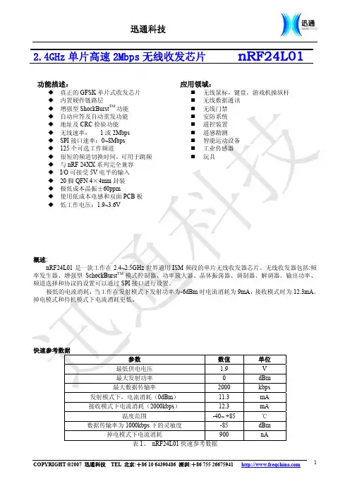
Rev. 1.2012021-10-13BC5602RF 2.4GHz收发器特性•频率带宽:2402~2480MHz •支持3线或4线SPI 接口 •输入电压范围宽:1.9V~3.6V•可编程数据速率:125/250/500Kbps•可编程TX 输出功率:5dBm (最大 +6dBm ) •低电流消耗♦Deep Sleep 模式电流0.5μA ,支持数据保存♦TX 电流:25mA @ 5dBm ♦RX 电流:17mA @ 250Kbps •两个Sleep 模式♦Middle Sleep 模式,支持快速XO 启动 ♦常规的Light Sleep 模式 •RX 灵敏度♦-97dBm @ 250Kbps 无线数据速率 •片上VCO 以及带内置回路滤波器的小数N 分频合成器•支持16MHz 晶振(±20ppm) •数据包处理 ♦数据白化♦自动应答/重发 ♦CRC 可选协议 ♦支持Burst 数据包 ♦支持自动ACK 处理♦适用于1:6星型网络的6个数据管道 •符合FCC/ETSI•封装类型:16-pin QFN (3mm ×3mm)概述BC5602为高性能、低成本的完全集成的CMOS RF GFSK 收发器,可用于2.4GHz 频 段的无线应用。
该芯片内置一个高集成的2.4GHz 收发器和一个基带调制解调器,可编程数据速率为125Kbps 、250Kbps 和500 Kbps 。
数据处理特性包括3层32字节TX/RX FIFO 和数据包处理,如白化和CRC 校验。
BC5602支持Middle Sleep 模式,仅消耗30μA 微量电流即可实现XO 快速启动。
该芯片可在2.4GHz 频段数据速率为250Kbps 时实现-97dBm 的灵敏度,提供+5dBm TX 输出功率时的电流消耗为25mA 。
完全内置的小数N 分频合成器所支持的频率范围宽,分辨率高。
外部主控MCU 可通过一个3线或4线的SPI 接口访问BC5602。
2.4G无线数传模块电路2.4G无线模块概述2.4G无线模块(英文:2.4Ghz RF transceiver ,receiver module)工作在全球免申请ISM频道2400M-2483M范围内,实现开机自动扫频功能,共有50个工作信道,可以同时供50个用户在同一场合同时工作,无需使用者人工协调、配置信道。
同时,可以根据成本考虑,选择50米内、150米、600 米多种类型无线模块。
接收单元和遥控器单元具有1键自动对码功能,数字地址编码,容量大,避免地址重复。
VT-CC2510-M1 无线模块采用TI chipcon高性能无线SOC芯片CC2510开发。
是一种完整的低成本、高度集成2.4GHz收发器,专为低功耗无线应用设计。
基本特点·高性能和低功耗的8051微控制器核·2400-2483.5MHz 低成本低功耗无线收发模块·SMD元件24mm×29mm×2.2 mm,内置PCB天线,体积小·支持2-FSK/GFSK/MSK·可编程控制的输出功率,对所有的支持频段可达+1dBm·可灵活配置多种通讯信道,快速频点切换特点,可满足跳频系统的需要·可编程配置传输数率1.2k - 500 kbps·低功耗3.3V 供电·RSSI输出和载波侦听指示几种2.4G无线数传模块介绍无线数传按传输速率区分,分为低速数传模块和高速数传模块两大类,低速数传模块使用的载频均较低,一般都在315MHz,433MHz和915MHz这几个频段,所以一般最高传输速率均不大于150kB/s。
但这些使用在UHF频段无线设备,载波仍具有一定的穿透和绕射能力,传送距离相对较远,最大可达数百米,这是它的优势,但同时也有其固存的缺点,因为工作频率低,工业干扰大,同时大量的汽车无线遥控(锁)均使用这个频段,干扰相对严重,这在技术上严。
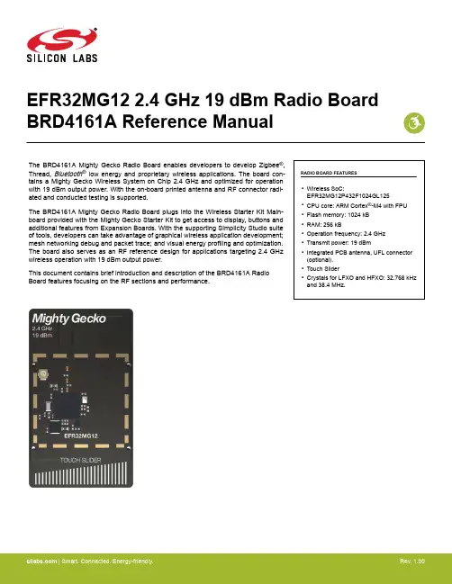
EFR32MG12 2.4 GHz 19 dBm Radio Board BRD4161A Reference ManualRADIO BOARD FEATURES•Wireless SoC:EFR32MG12P432F1024GL125•CPU core: ARM Cortex ®-M4 with FPU •Flash memory: 1024 kB •RAM: 256 kB•Operation frequency: 2.4 GHz •Transmit power: 19 dBm•Integrated PCB antenna, UFL connector (optional).•Touch Slider•Crystals for LFXO and HFXO: 32.768 kHz and 38.4 MHz.The BRD4161A Mighty Gecko Radio Board enables developers to develop Zigbee ®, Thread,Bluetooth ® low energy and proprietary wireless applications. The board con-tains a Mighty Gecko Wireless System on Chip 2.4 GHz and optimized for operation with 19 dBm output power. With the on-board printed antenna and RF connector radi-ated and conducted testing is supported.The BRD4161A Mighty Gecko Radio Board plugs into the Wireless Starter Kit Main-board provided with the Mighty Gecko Starter Kit to get access to display, buttons and additional features from Expansion Boards. With the supporting Simplicity Studio suite of tools, developers can take advantage of graphical wireless application development; mesh networking debug and packet trace; and visual energy profiling and optimization. The board also serves as an RF reference design for applications targeting 2.4 GHz wireless operation with 19 dBm output power.This document contains brief introduction and description of the BRD4161A Radio Board features focusing on the RF sections and performance.| Smart. Connected. Energy-friendly.Rev. 1.00Introduction 1. IntroductionThe EFR32 Mighty Gecko Radio Boards provide a development platform (together with the Wireless Starter Kit Mainboard) for the Silicon Labs EFR32 Mighty Gecko Wireless System on Chips and serve as reference designs for the matching network of the RF inter-face.The BRD4161A Radio Board is designed to operate in the 2400-2483.5 MHz band with the RF matching network optimized to operate with 19 dBm output power.To develop and/or evaluate the EFR32 Mighty Gecko, the BRD4161A Radio Board can be connected to the Wireless Starter Kit Main-board to get access to display, buttons and additional features from Expansion Boards and also to evaluate the performance of the RF interface.2. Radio Board Connector2.1 IntroductionThe board-to-board connector scheme allows access to all EFR32MG12 GPIO pins as well as the RESETn signal. For more informa-tion on the functions of the available pin functions, see the EFR32MG12 data sheet.2.2 Radio Board Connector Pin AssociationsThe figure below shows the pin mapping on the connector to the radio pins and their function on the Wireless Starter Kit Mainboard.GNDF9 / PA3 / VCOM_RTS 3v3VCOM_RTS / PA3 / P36P200Upper RowNC / P38NC / P40PF9 / P42PF11 / P44DEBUG.TMS_SWDIO / PF1 / F0DISP_ENABLE / PD15 / F14UIF_BUTTON0 / PF6 / F12UIF_LED1 / PF4 / F10VCOM_CTS / PA2 / F8DEBUG.RESET / RADIO_#RESET / F4DEBUG.TDO_SWO / PF2 / F2DISP_SI / PC6 / F16VCOM_TXD / PA0 / F6PTI_DATA / PB12 / F20DISP_EXTCOMIN / PD13 / F18USB_VBUS5VBoard ID SCLGNDBoard ID SDAUSB_VREG F7 / PA1 / VCOM_RXD F5 / PA5 / VCOM_ENABLE F3 / PF3 / DEBUG.TDIF1 / PF0 / DEBUG.TCK_SWCLK P45 / PF12P43 / PF10P41 / PF8P39 / NC P37/ PB10 / SENSOR_ENABLE F11 / PF5 / UIF_LED1F13 / PF7 / UIF_BUTTON1F15 / PC8 / DISP_SCLK F17 / PD14 / DISP_SCS F19 / PB13 / PTI_FRAME F21 / PB11 / PTI_CLK GND VMCU_IN PD8 / P0P201Lower RowPD9 / P2PD10 / P4PD11 / P6GNDNCP35 / PA2 / VCOM_CTS P7 / PA9P5 / PA8P3 / PA7P1 / PA6P33 / PA0 / VCOM_TXD P31 / PK2P29 / PK0P27 / PJ14P25 / PI2P23 / PI0P21 / PF14P19 / NC P17 / PC5P15 / PB9P13 / PC11P11 / PB7P9 / PB6VCOM_RXD / P34 / P34BODEN / P32PK1/ P30PJ15 / P28PI3 / P26PI1 / P24PF15 / P22PF13 / P20NC / P18PC4 / P16PB8 / P14PC10 / P12PC9 / P10PD12 / P8Figure 2.1. BRD4161A Radio Board Connector Pin MappingRadio Board Connector3. Radio Board Block Summary3.1 IntroductionThis section gives a short introduction to the blocks of the BRD4161A Radio Board.3.2 Radio Board Block DiagramThe block diagram of the EFR32MG Radio Board is shown in the figure below.Figure 3.1. BRD4161A Block Diagram3.3 Radio Board Block Description3.3.1 Wireless MCUThe BRD4161A Mighty Gecko Radio Board incorporates an EFR32MG12P432F1024GL125 Wireless System on Chip featuring 32-bit Cortex®-M4 with FPU core, 1024 kB of flash memory and 256 kB of RAM and a 2.4 GHz band transceiver with output power up to 19 dBm. For additional information on the EFR32MG12P432F1024GL125, refer to the EFR32MG12 Data Sheet.3.3.2 LF Crystal Oscillator (LFXO)The BRD4161A Radio Board has a 32.768 kHz crystal mounted.3.3.3 HF Crystal Oscillator (HFXO)The BRD4161A Radio Board has a 38.4 MHz crystal mounted.| Smart. Connected. Energy-friendly.Rev. 1.00 | 33.3.4 Matching Network for 2.4 GHzThe BRD4161A Radio Board incorporates a 2.4 GHz matching network which connects the 2.4 GHz TRX pin of the EFR32MG12 to the one on-board printed Inverted-F antenna. The component values were optimized for the 2.4 GHz band RF performace and current con-sumption with 19 dBm output power.For detailed description of the matching network, see Chapter 4.2.1 Description of the 2.4 GHz RF Matching.3.3.5 Inverted-F AntennaThe BRD4161A Radio Board includes a printed Inverted-F antenna (IFA) tuned to have close to 50 Ohm impedance at the 2.4 GHz band.For detailed description of the antenna see Chapter 4.5 Inverted-F Antenna.3.3.6 UFL ConnectorTo be able to perform conducted measurements, Silicon Labs added an UFL connector to the Radio Board. The connector allows an external 50 Ohm cable or antenna to be connected during design verification or testing.Note: By default the output of the matching network is connected to the printed Inverted-F antenna by a series component. It can be connected to the UFL connector as well through a series 0 Ohm resistor which is not mounted by default. For conducted measurements through the UFL connector the series component to the antenna should be removed and the 0 Ohm resistor should be mounted (see Chapter 4.2 Schematic of the RF Matching Network for further details).3.3.7 Radio Board ConnectorsTwo dual-row, 0.05” pitch polarized connectors make up the EFR32MG Radio Board interface to the Wireless Starter Kit Mainboard. For more information on the pin mapping between the EFR32MG12P432F1024GL125 and the Radio Board Connector, refer to Chapter 2.2 Radio Board Connector Pin Associations.3.3.8 Capacitive Touch SliderThe touch slider (T2) utilizes the capacitive touch capability of the Capacitance Sense Module of the EFR32MG12. The slider interpo-lates 4 separate pads to find the exact position of a finger.The figure below shows the pin mapping of the touch slider to the Wireless SoC.Wireless SoCFigure 3.2. Touch Slider Pin MappingRev. 1.00 | 44. RF Section4.1 IntroductionThis section gives a short introduction to the RF section of the BRD4161A.4.2 Schematic of the RF Matching NetworkThe schematic of the RF section of the BRD4161A Radio Board is shown in the following figure.2.4 GHz Matching 2.4 GHz RF OutputSelection & Inverted-F AntennaFigure 4.1. Schematic of the RF Section of the BRD4161A4.2.1 Description of the 2.4 GHz RF MatchingThe 2.4 GHz matching connects the 2G4RF_IOP pin to the on-board printed Inverted-F Antenna. The 2G4RF_ION pin is connected to ground. For higher output powers (13 dBm and above), besides the impedance matching circuitry, it is recommended to use additional harmonic filtering as well at the RF output. The targeted output power of the BRD4161A board is 19 dBm. Therefore, the RF output of the IC is connected to the antenna through a four-element impedance matching and harmonic filter circuitry.For conducted measurements the output of the matching network can also be connected to the UFL connector by removing the series R1 component between the antenna and the output of the matching and adding a 0 Ohm resistor to the R2 resistor position between the output of the matching and the UFL connector.4.3 RF Section Power SupplyOn the BRD4161A Radio Board the power supply pins of the RF section (RFVDD, PAVDD) are directly connected to the output of the on-chip DC-DC converter. This way, by default, the DC-DC converter provides 1.8 V for the entire RF section (for details, see the sche-matic of the BRD4161A).4.4 Bill of Materials for the 2.4 GHz MatchingThe Bill of Materials of the 2.4 GHz matching network of the BRD4161A Radio Board is shown in the following table.| Smart. Connected. Energy-friendly.Rev. 1.00 | 5Table 4.1. Bill of Materials for the BRD4161A 2.4GHz RF Matching Network4.5 Inverted-F AntennaThe BRD4161A Radio Board includes an on-board printed Inverted-F Antenna tuned for the 2.4 GHz band. Due to the design restric-tions of the Radio Board, the input of the antenna and the output of the matching network can't be placed directly next to each other. As a result, a 50 Ohm transmission line was necessary to connect them. With the actual line length the impedance of the antenna at the double-harmonic frequency is transformed closer to a "critical load impedance range" resulting in the radiated level of the harmonic increases.To reduce the harmonic radiation a tuning component was used between the matching network output and the antenna input. For the actual Radio Board design (with the actual transmission line length) a small value inductor was used (instead of the R1 resistor with value of 1.8 nH) to transform the impedance at the double-frequency harmonic away from the critical region while keeping the impe-dance at the funamental close to 50 Ohm. With this the suppression of the radiated double-frequency harmonic increases by approxi-mately 3-4 dB. The resulting impedance and reflection measured at the output of the matcing network are shown in the following figure. As it can be observed the impedance is close to 50 Ohm (the reflection is better than -10 dB) for the entire 2.4 GHz band.Figure 4.2. Impedance and Reflection of the Inverted-F Antenna of the BRD4161A Board Measured from the Matching Output Note: The same value and type of 1.8 nH inductor was used as the one in the matching network (L1). | Smart. Connected. Energy-friendly.Rev. 1.00 | 65. Mechanical DetailsThe BRD4161A Mighty Gecko Radio Board is illustrated in the figures below.Figure 5.1. BRD4161A Top View24 mmConnectorConnector Figure 5.2. BRD4161A Bottom ViewMechanical DetailsRev. 1.00 | 7EMC Compliance 6. EMC Compliance6.1 IntroductionCompliance of the fundamental and harmonic levels is tested against the following standards:• 2.4 GHz:•ETSI EN 300-328•FCC 15.2476.2 EMC Regulations for 2.4 GHz6.2.1 ETSI EN 300-328 Emission Limits for the 2400-2483.5 MHz BandBased on ETSI EN 300-328 the allowed maximum fundamental power for the 2400-2483.5 MHz band is 20 dBm EIRP. For the unwan-ted emissions in the 1 GHz to 12.75 GHz domain the specified limit is -30 dBm EIRP.6.2.2 FCC15.247 Emission Limits for the 2400-2483.5 MHz BandFCC 15.247 allows conducted output power up to 1 Watt (30 dBm) in the 2400-2483.5 MHz band. For spurious emmissions the limit is -20 dBc based on either conducted or radiated measurement, if the emission is not in a restricted band. The restricted bands are speci-fied in FCC 15.205. In these bands the spurious emission levels must meet the levels set out in FCC 15.209. In the range from 960 MHz to the frequency of the 5th harmonic it is defined as 0.5 mV/m at 3 m distance (equals to -41.2 dBm in EIRP).Additionally, for spurious frequencies above 1 GHz, FCC 15.35 allows duty-cycle relaxation to the regulatory limits. For the EmberZNet PRO the relaxation is 3.6 dB. Therefore, the -41.2 dBm limit can be modified to -37.6 dBm.If operating in the 2400-2483.5 MHz band the 2nd, 3rd and 5th harmonics can fall into restricted bands. As a result, for those the -37.6 dBm limit should be applied. For the 4th harmonic the -20 dBc limit should be applied.6.2.3 Applied Emission Limits for the 2.4 GHz BandThe above ETSI limits are applied both for conducted and radiated measurements.The FCC restricted band limits are radiated limits only. Besides that, Silicon Labs applies those to the conducted spectrum i.e., it is assumed that, in case of a custom board, an antenna is used which has 0 dB gain at the fundamental and the harmonic frequencies. In that theoretical case, based on the conducted measurement, the compliance with the radiated limits can be estimated.The overall applied limits are shown in the table below.Table 6.1. Applied Limits for Spurious Emissions for the 2.4 GHz Band | Smart. Connected. Energy-friendly.Rev. 1.00 | 87. RF Performance7.1 Conducted Power MeasurementsDuring measurements, the EFR32MG Radio Board was attached to a Wireless Starter Kit Mainboard which was supplied by USB. The voltage supply for the Radio Board was 3.3 V.7.1.1 Conducted Measurements in the 2.4 GHz bandThe BRD4161A board was connected directly to a Spectrum Analyzer through its UFL connector (the R1 component was removed and a 0 Ohm resistor was soldered to the R2 resistor position). During measurements, the voltage supply for the board was 3.3 V provided by the mainboard. The supply for the radio (RFVDD) was 1.8 V provided by the on-chip DC-DC converter, the supply for the power amplifier (PAVDD) was 3.3 V (for details, see the schematic of the BRD4161A). The transceiver was operated in continuous carrier transmission mode. The output power of the radio was set to 19 dBm.The typical output spectrum is shown in the following figure.Figure 7.1. Typical Output Spectrum of the BRD4161AAs it can be observed, the fundamental is slightly lower than 19 dBm limit and the strongest unwanted emission is the double-frequency harmonic and it is under the -37.6 dBm applied limit.Note: The conducted measurement is performed by connecting the on-board UFL connector to a Spectrum Analyzer through an SMA Conversion Adapter (P/N: HRMJ-U.FLP(40)). This connection itself introduces approximately 0.3 dB insertion loss.RF PerformanceRev. 1.00 | 97.2 Radiated Power MeasurementsDuring measurements, the EFR32MG Radio Board was attached to a Wireless Starter Kit Mainboard which was supplied by USB. The voltage supply for the Radio Board was 3.3 V. The radiated power was measured in an antenna chamber by rotating the DUT 360degrees with horizontal and vertical reference antenna polarizations in the XY , XZ and YZ cuts. The measurement axes are shown inthe figure below.Figure 7.2. DUT: Radio Board with the Wireless Starter Kit Mainboard (Illustration)Note: The radiated measurement results presented in this document were recorded in an unlicensed antenna chamber. Also the radi-ated power levels may change depending on the actual application (PCB size, used antenna, and so on). Therefore, the absolute levels and margins of the final application are recommended to be verified in a licensed EMC testhouse.7.2.1 Radiated Measurements in the 2.4 GHz bandFor the transmitter antenna the on-board printed Inverted-F antenna of the BRD4161A board was used (the R1 component was moun-ted). During measurements, the board was attached to a Wireless Starter Kit Mainboard (BRD4001 (Rev. A02) ) which was supplied through USB. During the measurements the voltage supply for the board was 3.3 V provided by the mainboard. The supply for the radio (RFVDD) was 1.8 V provided by the on-chip DC-DC converter, the supply for the power amplifier (PAVDD) was 3.3 V (for details, see the schematic of the BRD4161A). The transceiver was operated in continuous carrier transmission mode. The output power of the radio was set to 19 dBm based on the conducted measurement.The results are shown in the table below.Table 7.1. Maximums of the measured radiated powers in EIRP [dBm]As it can be observed, thanks to the high gain of the Inverted-F antenna, the level of the fundamental is higher than 19 dBm. The stron-gest harmonic is the double-frequency one and thanks to the additional suppression provided by the instead of the R1 resistor its level is under -50 dBm.RF PerformanceEMC Compliance Recommendations 8. EMC Compliance Recommendations8.1 Recommendations for 2.4 GHz ETSI EN 300-328 complianceAs it was shown in the previous chapter, the radiated power of the fundamental of the BRD4161A Mighty Gecko Radio Board complies with the 20 dBm limit of the ETSI EN 300-328 in case of the conducted measurement but due to the high antenna gain the radiated power is higher than the limit by 2 dB. In order to comply, the output power should be reduced (with different antennas, depending on the gain of the used antenna, the necessary reduction can be different). The harmonic emissions are under the -30 dBm limit. Although the BRD4161A Radio Board has an option for mounting a shielding can, that is not required for the compliance.8.2 Recommendations for 2.4 GHz FCC 15.247 complianceAs it was shown in the previous chapter, the radiated power of the fundamental of the BRD4161A Mighty Gecko Radio Board complies with the 30 dBm limit of the FCC 15.247. The harmonic emissions are under the -37.6 dBm applied limit both in case of the conducted and the radiated measurements. Although the BRD4161A Radio Board has an option for mounting a shielding can, that is not required for the compliance.Document Revision History 9. Document Revision HistoryTable 9.1. Document Revision HistoryBoard Revision History 10. Board Revision HistoryTable 10.1. BRD4161A Radio Board RevisionsErrata 11. ErrataThere are no known errata at present.Table of Contents1. Introduction (1)2. Radio Board Connector (2)2.1 Introduction (2)2.2 Radio Board Connector Pin Associations (2)3. Radio Board Block Summary (3)3.1 Introduction (3)3.2 Radio Board Block Diagram (3)3.3 Radio Board Block Description (3)3.3.1 Wireless MCU (3)3.3.2 LF Crystal Oscillator (LFXO) (3)3.3.3 HF Crystal Oscillator (HFXO) (3)3.3.4 Matching Network for 2.4 GHz (4)3.3.5 Inverted-F Antenna (4)3.3.6 UFL Connector (4)3.3.7 Radio Board Connectors (4)3.3.8 Capacitive Touch Slider (4)4. RF Section (5)4.1 Introduction (5)4.2 Schematic of the RF Matching Network (5)4.2.1 Description of the 2.4 GHz RF Matching (5)4.3 RF Section Power Supply (5)4.4 Bill of Materials for the 2.4 GHz Matching (5)4.5 Inverted-F Antenna (6)5. Mechanical Details (7)6. EMC Compliance (8)6.1 Introduction (8)6.2 EMC Regulations for 2.4 GHz (8)6.2.1 ETSI EN 300-328 Emission Limits for the 2400-2483.5 MHz Band (8)6.2.2 FCC15.247 Emission Limits for the 2400-2483.5 MHz Band (8)6.2.3 Applied Emission Limits for the 2.4 GHz Band (8)7. RF Performance (9)7.1 Conducted Power Measurements (9)7.1.1 Conducted Measurements in the 2.4 GHz band (9)7.2 Radiated Power Measurements (10)7.2.1 Radiated Measurements in the 2.4 GHz band (10)8. EMC Compliance Recommendations (11)8.1 Recommendations for 2.4 GHz ETSI EN 300-328 compliance (11)8.2 Recommendations for 2.4 GHz FCC 15.247 compliance (11)9. Document Revision History (12)10. Board Revision History (13)11. Errata (14)Table of Contents (15)Silicon Laboratories Inc.400 West Cesar Chavez Austin, TX 78701USASimplicity StudioOne-click access to MCU and wireless tools, documentation, software, source code libraries & more. Available for Windows, Mac and Linux!IoT Portfolio /IoTSW/HW/simplicityQuality/qualitySupport and CommunityDisclaimerSilicon Labs intends to provide customers with the latest, accurate, and in-depth documentation of all peripherals and modules available for system and software implementers using or intending to use the Silicon Labs products. Characterization data, available modules and peripherals, memory sizes and memory addresses refer to each specific device, and "Typical" parameters provided can and do vary in different applications. Application examples described herein are for illustrative purposes only. Silicon Labs reserves the right to make changes without further notice and limitation to product information, specifications, and descriptions herein, and does not give warranties as to the accuracy or completeness of the included information. Silicon Labs shall have no liability for the consequences of use of the information supplied herein. This document does not imply or express copyright licenses granted hereunder to design or fabricate any integrated circuits. The products are not designed or authorized to be used within any Life Support System without the specific written consent of Silicon Labs. A "Life Support System" is any product or system intended to support or sustain life and/or health, which, if it fails, can be reasonably expected to result in significant personal injury or death. Silicon Labs products are not designed or authorized for military applications. Silicon Labs products shall under no circumstances be used in weapons of mass destruction including (but not limited to) nuclear, biological or chemical weapons, or missiles capable of delivering such weapons.Trademark InformationSilicon Laboratories Inc.® , Silicon Laboratories®, Silicon Labs®, SiLabs® and the Silicon Labs logo®, Bluegiga®, Bluegiga Logo®, Clockbuilder®, CMEMS®, DSPLL®, EFM®, EFM32®, EFR, Ember®, Energy Micro, Energy Micro logo and combinations thereof, "the world’s most energy friendly microcontrollers", Ember®, EZLink®, EZRadio®, EZRadioPRO®, Gecko®, ISOmodem®, Precision32®, ProSLIC®, Simplicity Studio®, SiPHY®, Telegesis, the Telegesis Logo®, USBXpress® and others are trademarks or registered trademarks of Silicon Labs. ARM, CORTEX, Cortex-M3 and THUMB are trademarks or registered trademarks of ARM Holdings. Keil is a registered trademark of ARM Limited. All other products or brand names mentioned herein are trademarks of their respective holders.。
竭诚为您提供优质文档/双击可除2.4g无线通信协议篇一:无线技术知识2.4g无线技术知识2.4g与其他无线技术对比●从理论上来讲,2.4ghz是工作在ism频段的一个频段。
ism频段是工业,科学和医用频段。
一般来说世界各国均保留了一些无线频段,以用于工业,科学研究,和微波医疗方面的应用。
应用这些频段无需许可证,只需要遵守一定的发射功率(一般低于1w),并且不要对其它频段造成干扰即可。
●ism频段在各国的规定并不统一。
而2.4ghz为各国共同的ism频段。
因此无线局域网(ieee802.11b/ieee802.11g),蓝牙,zigbee等无线网络,均可工作在2.4ghz频段上。
●大家所谓的2.4g无线技术,其频段处于2.405ghz-2.485ghz(科学、医药、农业)之间。
所以简称为2.4g无线技术。
●2.4g免费频段是什么意思免费频段,是指各个国家根据各自的实际情况,并考虑尽可能与世界其他国家规定的一致性,而划分出来的一个频段,专门用于工业,医疗以及科学研究使用(ism频段),不需申请而可以免费使用的频段。
我们国家的2.4g频段,就是这样一个频段。
然而,为了保证大家都可以合理使用,国家对该频段内的无线收发设备,在不同环境下的使用功率做了相应的限制。
例如在城市环境下,发射功率不能超过100mw。
●2.4g无线键鼠收发模块挪威著名芯片厂商的nRF24l01无线收发芯片nRF24l01是单片射频收发芯片,工作于2.4~2.5ghzism 频段。
工作电压为1.9~3.6V,有多达125个频道可供选择。
可通过spi写入数据,最高可达10mb/s,数据传输率最快可达2mb/s,并且有自动应答和自动再发射功能。
和上一代nRF2401相比,nRF24l01数据传输率更快,数据写入速度更高,内嵌的功能更完备。
芯片能耗非常低,以-6dbm的功率发射时,工作电流只有9ma,接收时工作电流只有12.3ma,多种低功率工作模式(掉电模式和空闲模式)使节能设计更方便。
第一章概述 (3)1.1产品简介 (3)1.2功能特点 (3)1.3设备类型介绍 (4)1.3.1 非休眠终端 (4)1.3.2 休眠终端 (4)1.4 应用场景 (4)第二章规格参数 (5)2.1 极限参数 (5)2.2 工作参数 (5)第三章机械尺寸与引脚定义 (6)第四章工作模式 (7)4.1 传输模式 (7)4.2 配置模式 (8)4.3 模式切换 (8)4.3.1 指令切换 (8)4.3.2 引脚切换 (8)第五章收发方式 (8)5.1数据发送的方式 (8)5.1.1广播模式 (8)5.1.2 组播模式 (9)5.1.3 单播模式 (9)5.2 接收数据的输出方式 (9)5.2.1 透明输出 (9)5.2.2 数据+短地址 (9)5.2.3 数据+长地址 (9)5.2.4 数据+RSSI (9)5.2.5 数据+短地址+RSSI (9)5.2.6 数据+长地址+RSSI (10)第六章应用功能和指令配置 (10)6.1 功能引脚 (10)6.1.1 LINK 详解 (10)6.1.2 WAKE详解 (10)6.1.3 AUX详解 (10)6.1.4 ACK详解 (10)6.1.5 UART_BAUD_RESET详解 (10)6.2 无线远程配置功能 (11)6.3功能参数说明 (11)6.5 HEX指令集 (12)6.5.1 指令规则 (12)6.5.2 读取指令集 (13)6.5.2 配置指令集 (15)6.5.3 网络操作指令集 (16)6.6 HEX 参数说明 (17)6.6.1 系统发送模式 (17)6.6.2 接收数据输出方式 (17)6.6.3网络节点类型 (17)6.6.4网络状态 (17)6.6.5网络 PAN_ID (18)6.6.6网络短地址: (18)6.6.7 MAC 地址 (18)6.6.8父节点网络短地址 (18)6.6.9父节点 MAC 地址 (18)6.6.10网络组号 (18)6.6.11网络信道 (18)6.6.12发送功率 (18)6.6.13串口波特率 (19)6.6.14休眠时间 (19)6.6.15父节点保存时间 (19)6.6.16父节点丢失后网络重连的周期 (19)6.6.17尝试重连的最大次数 (19)6.6.18无线远程配置ID (20)6.6.19用户 gpio 参数 (20)6.6.20用户 pwm 参数 (20)6.6.21用户 adc 参数 (21)6.6.22 配置所有网络参数 (21)6.6.23 读取所有网络参数 (21)第七章快速入门 (22)7.1 快速建立一个ZigBee网络 (22)7.2 快速加入一个ZigBee网络 (25)7.3 ZigBee网络通信测试 (28)7.3.1单播测试 (28)7.3.1.1终端和协调器之间相互以短地址形式单播 (28)7.3.1.2终端和协调器之间相互以长地址形式单播 (29)7.3.2组播测试 (30)7.3.3广播测试 (32)第九章常见问题 (33)9.1 传输距离不理想 (33)9.2 模块易损坏 (33)9.3 误码率太高 (33)关于我们 (34)第一章概述1.1产品简介E180-Z6907A是基于TELINK TLSR8269无线SOC设计生产的一款小体积、低功耗、高可靠性、工作在2.4GHz 频段的ZIGBEE模块,芯片自带高达48Mhz的32位高性能MCU,发射功率最高可达到7dBm。
无线SoC芯片(CC1010,nRF9E5,nRF24E1)对比分析本文来自: 原文网址:/info/commonIC/0073686.html随着网络及其通信技术的飞速发展,短距离无线通信以其抗干扰能力强、可靠性高、安全性好、受地理条件限制较少、安装施工简便灵活等特点,在许多领域都得到了广泛的应用。
无线SoC芯片(也称无线单片机)将微控制器、存储器、A/D转换器、需要的接口电路和无线收发芯片全部集成到一个非常小的芯片上,并具有通用频带、收发合一、低发射功率、高灵敏接收等优点,因而在当前短距离无线通信系统中的应用潜力十分巨大。
而采用内嵌8051的无线SoC芯片,一方面能继续使用8051微控制器已经发展成熟的各种应用软件资源。
另一方面,目前市面上流行的8051开发工具(如Keil C51)都可以用于这种芯片的软件开发。
在已经推出的几种以8051微控制器为内核的无线SoC芯片中。
最具有代表性的是chipcon公司的CC1010、Nordic公司的nRF9E5和nRF24E1。
本文将对这三款无线SoC芯片作以对比描述,同时分析一下它们各自的结构原理、特性及典型应用电路1 CC1010无线SoC芯片CC1010是Chipcon公司推出的单片、多频段、低功耗的系统级无线射频收发芯片。
该芯片基于Chipcon公司的0.35 um CMOS工艺生产,具有很高的集成度该芯片内嵌8051微控制器,并包含32 KB Flash、2048+128字节SRAM、3通道10位ADC以及加密/解密用的DES模块。
发射器采用直接变频发射,接收器采用低-中变频接收。
CC1010通过8位控制寄存器RFMAIN来实现无线收发控制,不同工作频率(315-915 MHz)的应用电路可通过调节元器件C31~C181、L32~L101和R131等参数值来实现外接晶体必须连接到芯片的XOSC端,同时VCO也需要外接一个外部电感。
CC1010的典型应用电路如图1所示。
在短距离的通信中,无线技术被普遍看好,其中射频技术因其功耗低和无方向性等优点而受到青睐。
通信频率为2.4GHz的频段是全球开放的ISM(工业、科学和医学)频段,人们无需申请许可证即可使用,给开发者和用户带来了很大方便;同时,该频率又可以有效地避免低频段信号、各类电火花以及家用电器等的干扰。
由于这一频段具有的优点,其他的一些应用,例如蓝牙(BlueTooth)、无线局域网(WLAN)也在这一频段;但蓝牙和无线局域网对于工业控制、医疗传感器、智能自动化装置等设备来说,过于复杂,其成本也过高,很难满足快速开发和低成本的要求。
因此,目前迫切需要一种低成本、低功耗、能够快速开发应用的方案,实现设备的无线连接。
本文结合无线片上系统NRF24El芯片的具体系统开发实例,研究一种无线组网技术。
1 无线片上系统NRF24E1NRF24E1 是一种工作频率可达到2.4GHz的无线射频收发芯片。
内部嵌有与8051 兼容的微处理器和10位9路A/D转换器,可以在 1.9~3.6V电压下稳定工作。
其内部还有电压调整器和VDD电压监视,通道转换时间小于200微秒,数据速率1Mbps,不需要外接SAW 滤波器。
NRF24E1是目前首次推出的全球2.4GHz通用的、完整低成本射频系统级芯片。
无线收发部分有与nRF2401同样的功能。
该功能由外部并行口和外部SPI 启动,每一个待发信号对于处理器来讲都可以作为中断来编程,或者通过GPIO端口实现。
NRF24E1是一个可以在全球公用的频段范围(2.4~2.5 GHz)内实现无线通信的芯片。
收发机包含 1 个完全集成的分频器、放大器、调节器和 2 个收发单元。
输出能量、频段等射频参数,可通过射频寄存器方便地编程调节。
在发送模式下,电流消耗只有10.5mA;在接收模式下,只有18mA,所以功耗相当低。
图1是NRF24E1芯片示意图。
从图中看到,NRF24E1由一个8051微控制器内核和一个NRF2401 无线收发器组成,芯片包括:增强型8051 内核、无线收发器NRF2401、9路100ksps的10位模数转换器、UART 异步串口、SPI 接口、PWM 输出、RC振荡器、看门狗和唤醒定时器以及内置的专用稳压电路等。
发布时间:2012-11-01 16:54:202.4GRF协议BLE蓝牙4.0协议芯片NRF51822介绍技术类别:资源共享关于 nRF51 系列多协议 2.4GHz 射频收发器拥有高性能、超低功耗以及灵活性等好处。
它的主要功能包括:在蓝牙低功耗模式下灵敏度为-92.5dB RX,高达 +4dBm 的输出功率;与 Nordic 上一代射频收发器相比,链接预算增强高达 9.5dBm;低于10mA 的峰值电流适合3V 纽扣电池;符合蓝牙低功耗(蓝牙 4.0 )标准;与 Nordic 现有的 nRF24L 系列 IC 空中完全兼容;支持包括蓝牙低功耗、ANT 和专有 2.4GHz 等协议的非并行和并行操作;场强RSSI。
nRF51 系列 SoC 大大地降低平均电流,使单芯片适用于各种无线应用。
它的主要功能包括:功能强大且低功耗的 32 位 ARM Cortex-M0 处理器,启动时间为 2µs,与 8/16 位处理器相比,大限度地降低了活动时间并提高了代码密度;细化电源管理,个别系统可独立开关,并能基于活动级别自主控制时钟;可编程周边互连 (PPI) 系统。
周边设备,如射频收发器、计时器及 I/O等,不需通过处理器而能自主相互作用。
从而降低处理器的活动时间来节省功耗,并放宽对处理器实时要求。
高效的EasyDMA射频收发器接口具有弹性 RAM 映射 FIFO;高灵活性的GPIO 映射简化了 PCB 设计,有助降低布线板层数量;自定义 2 区内存保护装置 (MPU) 对用户程序和预编译协议堆栈例如蓝牙低功耗和 ANT运行时保护。
nRF51 系列软件架构在协议堆栈和用户应用程序间具有一个独特且功能强大的分隔区,为应用程序开发人员提供最大的灵活性、开发简易性和代码安全性。
协议堆栈,例如蓝牙低功耗或 ANT,可为预编译二进制码或在设备上预编程;堆栈为 100% 异步并由事件驱动,并向应用程序层提供线程安全管理程序调用 (SVC) 的应用程序接口 (API);简单的编程模型,没有专用的应用程序框架或计划程序/RTOS 依存性,简化并加速了代码开发;协议堆栈和应用程序代码没有链接时间依存性,并可独立编译和更新/编程;堆栈受运行时保护,确保相互操作性并将应用程序错误而影响堆栈的风险降低;堆栈可以验证码和合格二进制目的码提供。
nRF24L01的工作原理nRF24L01是一款低功耗的2.4GHz无线收发器,广泛应用于无线通信领域。
它采用射频芯片nRF24L01+和微控制器相结合的方式,可以实现无线数据传输和接收功能。
本文将详细介绍nRF24L01的工作原理及其相关技术参数。
一、nRF24L01的基本结构nRF24L01由射频芯片和微控制器组成,射频芯片负责无线通信的收发功能,而微控制器则负责控制和处理数据。
1. 射频芯片nRF24L01射频芯片是一款集成度高、性能稳定的射频收发器。
它支持2.4GHz 频段,采用GFSK调制方式,具有快速的数据传输速率和较低的功耗。
射频芯片包含了射频收发器、调制解调器、频率合成器等功能模块,能够实现无线通信的基本功能。
2. 微控制器nRF24L01通常与微控制器相结合使用,常见的微控制器有Arduino、STM32等。
微控制器负责控制射频芯片的工作模式、发送和接收数据的处理,以及与其他设备的交互等功能。
二、nRF24L01的工作模式nRF24L01具有多种工作模式,包括发送模式、接收模式和待机模式等。
下面将详细介绍每种工作模式的特点和工作原理。
1. 发送模式在发送模式下,nRF24L01将数据发送给接收端。
发送模式的工作原理如下:- 设置发送端的地址和通信频道。
- 将待发送的数据写入发送缓冲区。
- 发送端开始发送数据,nRF24L01将数据通过射频信号发送出去。
- 发送完毕后,发送端等待接收端的应答信号。
2. 接收模式在接收模式下,nRF24L01接收来自发送端的数据。
接收模式的工作原理如下:- 设置接收端的地址和通信频道。
- 接收端开始监听射频信号,并等待发送端发送数据。
- 当接收端接收到数据时,nRF24L01将数据写入接收缓冲区。
- 接收端可以通过读取接收缓冲区中的数据进行进一步处理。
3. 待机模式在待机模式下,nRF24L01处于低功耗状态,仅保持最基本的功能。
待机模式的工作原理如下:- nRF24L01关闭射频发送和接收功能,以降低功耗。
产品概述E28系列产品是公司设计生产的2.4GHz射频收发模块,通信距离远;具有极低的低功耗模式流耗。
此模块为小体积贴片型(引脚间距1.27mm),模块自带高性能PCB板载天线。
E28系列产品采用Semtech公司的SX1280射频芯片,此芯片包含多样的物理层以及多种调制方式,如LORA,FLRC,GFSK。
特殊的调制和处理方式使得LORA和FLRC调制的传输距离大大增加;是一款高性能物联网无线收发器,并可以兼容蓝牙协议。
出色的低功耗性能、片上DC-DC和Time-of-flight使得此芯片功功能强大,可用于智能家居、安全系统、定位追踪、无线测距、穿戴设备、智能手环与健康管理等等。
SX1280支持RSSI,用户可以根据需要实现深度的二次开发;SX1280亦集成飞行时间(time of flight),适用于测距功能。
E28系列产品为硬件平台,无法独立使用,用户需要进行二次开发。
产品型号载波频率发射功率参考距离(PCB/IPX)封装形式天线形式E28(2G4M12S) 2.4GHz12.5dBm3000m贴片IPX/PCBE28(2G4M20S) 2.4GHz20dBm6000m贴片IPX/PCB 1.技术参数产品型号核心IC尺寸模块净重工作温度工作湿度储存温度E28(2G4M12S)SX128025*14*0.8mm0.9±0.1g-40~85℃10~90-40~125°C E28(2G4M20S)SX128026.5*15*2.8mm 1.2±0.1g-40~85℃10~90-40~125°C 1.1.E28(2G4M12S)参数类别Min Typ Max单位发射电流424550mA接收电流91011mA关断电流123μA发射功率1212.514dBm接收灵敏度-126-128-130dBm 推荐工作频段240024302500MHz 供电电压 1.8 3.3 3.6V通信电平 1.8 3.3 3.6V1.2.E28(2G4M20S)因采用高增益PA,为保证线性度和效率,SX1280不需配置为最大功率输出,建议SX1280的功率输出寄存器设置成16(输出功率为-2dBm)。
XN297L 系列产品说明书2.4GHz 单片高速无线收发芯片概述XN297L系列芯片是工作在2.400~2.483GHz世界通用ISM频段的单片无线收发芯片。
该芯片集成射频收发机、频率发生器、晶体振荡器、调制解调器等功能模块,并且支持一对多组网和带ACK的通信模式。
发射输出功率、工作频道以及通信数据率均可配置。
芯片已将多颗外围贴片阻容感器件集成到芯片内部。
主要特性1、功耗较低发射模式(2dBm)工作电流19mA;接收模式工作电流15mA;休眠电流2uA。
2、节省外围器件支持外围5个元器件,包括1颗晶振和4个贴片电容;支持双层或单层印制板设计,可以使用印制板微带天线;芯片自带部分链路层的通信协议;配置少量的参数寄存器,使用方便。
3、性能优异250K / 1M / 2M bps模式的接收灵敏度为-91 / -87 / -83dBm;发射输出功率最大可达13dBm;抗干扰性好,接收滤波器的邻道抑制度高,接收机选择性较好。
其它特性应用方案目录1 命名规则 (4)1.1 XN297L 命名规则 (4)1.2 XN297L 系列产品选择 (4)2 主要电特性 (4)3 极限最大额定值 (3)4 系统结构方框图 (4)5 引脚定义 (5)6 芯片工作状态 (6)6.1 休眠模式 (8)6.2 待机模式-I(STB1) (8)6.3 待机模式-III(STB3) (8)6.4 待机模式-II(STB2) (8)6.5 接收模式 (9)6.6 发射模式 (9)7 数据通信模式 (9)7.1 普通模式 (11)7.2 增强模式 (11)7.3 增强发送模式 (12)7.4 增强接收模式 (12)7.5 增强模式下的数据包识别 (13)7.6 增强模式下的PTX 和PRX 的时序图 (13)7.7 增强模式下的接收端一对多通信 (14)7.8 DATA F I F O (15)7.9 中断引脚 (16)8 SPI 控制接口 (16)8.1 SPI 指令格式 (16)8.2 SPI 时序 (18)9 控制寄存器 (20)10 数据包格式描述 (36)10.1 普通模式的数据包形式 (36)10.2 增强模式的数据包形式 (36)10.3 增强模式的ACK 包形式 (37)11 典型应用电路(参考) (37)12 封装尺寸 (38)13 联系方式 (39)1 命名规则1.1 XN297L 命名规则图1 X N297L系列芯片命名规则1.2 XN297L 系列产品选择表1 XN297L系列产品选择2 主要电特性表2 XN297L系列芯片主要电特性频道的接收灵敏度退化 2dB;发射信号调制精度(EVM)退化10%。
竭诚为您提供优质文档/双击可除2.4g无线通信协议篇一:无线技术知识2.4g无线技术知识2.4g与其他无线技术对比●从理论上来讲,2.4ghz是工作在ism频段的一个频段。
ism频段是工业,科学和医用频段。
一般来说世界各国均保留了一些无线频段,以用于工业,科学研究,和微波医疗方面的应用。
应用这些频段无需许可证,只需要遵守一定的发射功率(一般低于1w),并且不要对其它频段造成干扰即可。
●ism频段在各国的规定并不统一。
而2.4ghz为各国共同的ism频段。
因此无线局域网(ieee802.11b/ieee802.11g),蓝牙,zigbee等无线网络,均可工作在2.4ghz频段上。
●大家所谓的2.4g无线技术,其频段处于2.405ghz-2.485ghz(科学、医药、农业)之间。
所以简称为2.4g无线技术。
●2.4g免费频段是什么意思免费频段,是指各个国家根据各自的实际情况,并考虑尽可能与世界其他国家规定的一致性,而划分出来的一个频段,专门用于工业,医疗以及科学研究使用(ism频段),不需申请而可以免费使用的频段。
我们国家的2.4g频段,就是这样一个频段。
然而,为了保证大家都可以合理使用,国家对该频段内的无线收发设备,在不同环境下的使用功率做了相应的限制。
例如在城市环境下,发射功率不能超过100mw。
●2.4g无线键鼠收发模块挪威著名芯片厂商的nRF24l01无线收发芯片nRF24l01是单片射频收发芯片,工作于2.4~2.5ghzism 频段。
工作电压为1.9~3.6V,有多达125个频道可供选择。
可通过spi写入数据,最高可达10mb/s,数据传输率最快可达2mb/s,并且有自动应答和自动再发射功能。
和上一代nRF2401相比,nRF24l01数据传输率更快,数据写入速度更高,内嵌的功能更完备。
芯片能耗非常低,以-6dbm的功率发射时,工作电流只有9ma,接收时工作电流只有12.3ma,多种低功率工作模式(掉电模式和空闲模式)使节能设计更方便。
1.引言计的信号范围、音质和最长播放时间方面面临着重大挑战。
为满足这些要求,工程师可以利用来自多家制造商的大量可用产品,包括(按字母顺序)Analog在典型的无线娱乐系统(图1)中,源信号通过带有可选范围扩展器的无线射频接口传输到播放器系统,例如立体声耳机或扬声器。
在播放器内,相应的无线射频接口接收信号以供编解码器、音频处理器或 DSP 处理,以创建驱动到扬声器的最终模拟信号。
一个适当的电源,通常包括一个电池和充电管理电路,完成了系统。
子系统的可用集成解决方案可以帮助工程师满足这些要求,同时降低设计复杂性和成本。
2.频带遗留问题、市场接受度和未授权带宽的可用性通常会推动无线电通信频率的选择。
同时,满足增加操作范围和延长电池寿命的要求为有用频段设置了界限。
对增加功率的需求是对更远距离操作的渴望的自然结果,但射频波长的选择在平衡范围和功率方面起着至关重要的作用。
射频波长和范围之间的关系在Friis 传输方程中进行了描述:其中Pt = 发射功率Pr = 接收功率Gt = 发射器天线增益Gr = 接收器天线增益λ = 波长d = 发射器和接收器之间的距离对于统一参数,距离成为波长的简单线性函数,因此更长波长的无线电通信等同于更大的范围。
当然,更长的波段面临着包括干扰和有效载荷带宽在内的问题。
在这种情况下,2.4 GHz ISM 频段在实际范围限制和有用带宽之间提供了良好的平衡。
2.4 GHz 解决方案的吸引力在于它们能够以低功耗提供有用的有效范围,以及它们的全球可用性。
在蓝牙等标准中使用的基于跳频扩频(FHSS)的2.4 GHz 设计具有在高度活跃的无线电环境中相对不受干扰信号影响的优势。
与较低的ISM 频段相比,这些系统还提供足够的数据带宽,以允许高质量立体声的数字传输,后者通常仅限于模拟或较低数据速率的数字音频。
蓝牙标准工作频率为 2.4 GHz,非常适合消费者的连接要求。
它的广泛使用使得基于蓝牙的无线音频播放器很可能会找到兼容的音频主机,例如计算机、笔记本电脑、平板电脑和智能手机。
PL1167单片低功耗高性能 2.4GHz无线射频收发芯片芯片概述:主要特点:PL1167是一款工作在 2.4~2.5GHz 世界通用 ISM频段的单片低功耗高性能 2.4GHz无线射频收发芯片。
ψ 低功耗高性能2.4GHz无线射频收发芯片ψ 无线速率:1Mbps 该单芯片无线收发器集成包括:频率综合器、功率放大器、晶体振荡器、调制解调器等模块。
ψ 内置硬件链路层ψ 内置接收强度检测电路输出功率、信道选择与协议等可以通过 SPI或 I2C接ψ 支持自动应答及自动重发功能ψ 内置地址及FEC、CRC校验功能ψ 极短的信道切换时间,可用于跳频ψ 使用微带线电感和双层PCB板ψ 低工作电压:1.9~3.6V口进行灵活配置。
支持跳频以及接收强度检测等功能,抗干扰性能强,可以适应各种复杂的环境并达到优异的性能。
内置地址及 FEC、CRC校验功能。
ψ 封装形式:QFN16/TSSOP16 内置自动应答及自动重发功能。
ψψQFN16仅支持SPI接口芯片发射功率最大可以达到 5.5dBm,接收灵敏度可以达到-88dBm。
TSSOP16可支持SPI与I2C接口内置电源管理功能,掉电模式和待机模式下待机电流可以减小到接近 1uA。
应用:ψ 无线鼠标,键盘,游戏机操纵杆ψ 无线数据通讯ψ 无线门禁管脚分布图:ψ 无线组网ψ 安防系统ψ 遥控装置ψ 遥感勘测ψ 智能运动设备ψ 智能家居ψ 工业传感器ψ 工业和商用近距离通信ψ IP电话,无绳电话ψ 玩具1概要性能强,可以适应各种复杂的环境并达到优异的 性能。
PL1167 是一款工作在 2.4~2.5GHz 世界通 用 ISM 频段的单片低功耗高性能 2.4GHz 无线射 频收发芯片。
内置地址及 FEC 、CRC 校验功能。
该单芯片无线收发器集成包括:频率综合器、 功率放大器、晶体振荡器、调制解调器等模块。
内置自动应答及自动重发功能。
芯片发射功率最大可以达到 5.5dBm ,接收 灵敏度可以达到-88dBm 。
输出功率、信道选择与协议等可以通过 SPI 或 I2C 接口进行灵活配置。
内置电源管理功能,掉电模式和待机模式下 待机电流可以减小到接近 1uA 。
支持跳频以及接收强度检测等功能,抗干扰2特性ζ 低功耗高性能2.4GHz 无线射频收发芯片 ζ 无线速率:1Mbps ζ 极短的信道切换时间,可用于跳频 ζ 使用微带线电感和双层PCB 板 ζ 低工作电压:1.9~3.6V ζ 内置硬件链路层 ζ 内置接收强度检测电路ζ 封装形式:QFN16/TSSOP16 ζ 支持自动应答及自动重发功能 ζ 内置地址及FEC 、CRC 校验功能ζ ζQFN16仅支持SPI 接口 TSSOP16可支持SPI 与I2C 接口3快速参考数据参数数值单位最低工作电压 最大发射功率 数据传输速率 发射模式功耗@0dBm 接收模式功耗 工作温度范围 接收灵敏度 1.9 V dBm Mbps mA 5.5 1 16 17 -40 to +85-88 mA ℃ dBm uA掉电模式功耗14管脚分布图QFN16 管脚分布图如下:说明:MODE管脚在芯片内连接到VSS,因此QFN16仅支持SPI接口。
TSSOP16 管脚分布图如下:5管脚描述Pin(QFN16) 管脚名类型描述1 ANTBANT 天线天线接口2 天线天线接口3,8,17 VSS 电源接地(0V)4,5 6 N/C 悬空悬空不接PKT 数字输出数字输入数字输入发射/接收包状态指示位复位脚,低电平有效7 RSTBSCSB9 SPI接口从模式使能信号,低电平有效从SLEEP模式唤醒芯片10111213141516 SCKSDI数字输入数字输入数字输出电源SPI接口时钟输入SPI接口数据输入SPI接口数据输出(无效时为三态)电源(3.3V)SDOVCCVDDOXOUTXIN电源 1.8V内部LDO输出,外接电容晶振输出模拟输出模拟输入晶振输入Pin(TSSOP16) 管脚名类型描述1 2 3 4 5 6 AVSSN/C电源接地(0V)悬空悬空不接PKT 数字输出数字输入发射/接收包状态指示位复位脚,低电平有效接地(0V)RSTBDVSSSCSB电源数字输入SPI:SPI接口从模式使能信号,低电平有效从SLEEP模式唤醒芯片I2C:从SLEEP模式唤醒芯片SCK:SPI接口时钟输入7 8 9 SCK/SCL 数字输入SCL:I2C接口时钟输入SDI/A4 数字输入SDI:SPI接口数据输入A4:I2C接口地址位4SDO/SDA 数字输出数字I/OSDO:SPI接口数据输出(无效时为三态)SDA:I2C接口数据输入输出I/O接口模式选择:10 MODE 数字输入Pin(TSSOP16) 管脚名类型描述VSS :选择SPI 接口 VCC :选择I2C 接口11 12 13 14 15 16VCC 电源 电源(3.3V)VDDO XOUT XIN 电源 1.8V 内部LDO 输出,外接电容 晶振输出 模拟输出 模拟输入 天线 晶振输入 ANTB ANT天线接口 天线天线接口6结构框图7最大额定值参数符号范围单位VCC 供电电压VCC-0.3 to +3.6V参数符号VDDO V IN 范围单位V VDDO 供电电压 输入电压 输出电压 工作温度 仓储温度-0.3 to +2.5 -0.3 to (VCC+0.3) -0.3 to (VCC+0.3)-40 to +85 V V OUT T OP ℃ ℃T ST-40 to +125注释:超过最大额定值可能损毁器件;超过推荐工作范围的芯片功能特性不能保证;长时间工作于 最大额定条件下可能会影响器件的稳定性。
8电气特性(VCC=+3V ,VSS=0V ,TA=-40℃ to +85℃)符号参数(条件)说明 最小值 典型 最大值 单位工作条件 VCC T OPVCC 供电电压 1.9 -403.33.6 85V 工作温度 ℃数字输入管脚V IH V IL高电平输入电压 低电平输入电压 0.8VCC 0 1.2VCC 0.2VCC V V数字输出管脚V OH V OL高电平输出电压 低电平输出电压 0.8VCC 0VCC V V0.2VCC 常规射频条件f OP 工作频段 24002482MHz MHz KHz f XTAL 晶振频率12 △f 1M R GFSK F CHANNEL频率偏移@1Mbps 数据传输速率 信道间隔 280 1 Mbps MHz1 发射操作P RF 最大输出功率 05.5 22 dBm dB P RFC P RF1 P RF2 I VCC_H I VCC_L射频功率控制范围 第一临近信道发射功率 第二临近信道发射功率 高增益时功耗 1820-20 -50dBm dBm mA 16 12低增益时功耗 mA 接收操作 I VCC 接收功耗17 mA RX SENS0.1% BER 时接收灵敏度-88dBm9 SPI 接口9.1 SPI 接口说明PL1167收发芯片提供简单的 MCU 接口 SPI 模式,芯片的 SPI 接口只支持从模式。
SPI 接口包含 7个相关信号,如下表:管脚描述RSTB MODE SCSB 复位脚,低电平有效模式选择,为 0时选择 SPI 模式 SPI 接口从模式使能信号,低电平有效 从SLEEP 模式唤醒芯片 SPI 接口时钟输入 SCK SDI SPI 接口数据输入 SDO PKTSPI 接口数据输出 发射/接收包状态指示位9.2 SPI 命令格式符号最小 典型 最大 描述T SSH250ns两次 SPI 命令时间间隔符号最小典型最大描述T ,T SSR 41.5ns*1 SCSB与 SCK时间间隔SSFT A2D T H2L T R2R T SCK地址与数据时间间隔高低字节数据时间间隔两个寄存器数据时间间隔SCK时钟周期*1*183ns注:*1—在读 FIFO数据时,至少需要 450ns等待时间;其它寄存器时 T3min = 41.5ns。
10 I2C接口10.1 I2C接口说明管脚RSTB MODE SCSB SCL 描述复位脚,低电平有效模式选择,为 1时选择 I2C模式从 SLEEP模式唤醒芯片I2C接口时钟输入I2C数据输入输出 I/OI2C接口地址位 4SDAA410.2 I2C支持特性I2C从模式选择支持与否标准模式– 100 kbps快速模式– 400 kbps增强型快速模式– 1000 kbps 高速模式– 3200 kbps时钟展宽是是是否否否否否否10位从地址广呼方式地址软件复位器件 ID10.3 I2C命令格式10.4 I2C器件地址A6 A5 A4 A3 A2 A1 A0 R/W0 1 A4 Pin 1 0 0 0 Read=1Write=011控制寄存器最新的推荐控制寄存器值参考《用户手册》,请联系供应商索取。
12典型应用13封装QFN16 封装QFN16(4x4mm, 0.65mm pitch, Thinner) 封装尺寸TSSOP16 封装TSSOP16封装尺寸14注意事项为了持续改进产品的可靠性、功能或设计,保留随时更新修改的权利,并不另行通知客户。
客户在下单前请确认所使用的是最新的完整版说明书。