PL1167中文资料-2.4GHz无线射频收发芯片资料
- 格式:doc
- 大小:834.50 KB
- 文档页数:12
LL217-TX模组集成 2.4G无线收发及低功耗无线收发及低功耗 8bit MCU微处理器,工作在微处理器,工作在 2400MHz-2483.5MHz全球通用全球通用 ISM频段。
最大发射功率频段。
最大发射功率频段。
最大发射功率 2dBm,接收灵敏度,接收灵敏度 -92dBm。
LL217-TX内嵌无线跳频内嵌无线跳频抗干扰收发传输协议收发传输协议,无需进行二次开发,使用简无需进行二次开发,使用简无需进行二次开发,使用简单快捷。
LL217-TX 支持独立 8通道的开关量传输。
应用范围:
⚫无线遥控器
⚫遥控玩具
⚫安防系统
⚫有源 RFID
⚫ LED灯
主要参数:
⚫供电压: 2.2V~3.6V
⚫最大发射功率: 2dBm
⚫遥控器工作电流:5mA
⚫休眠电流:小于 5uA
⚫调制方式: GFSK
⚫空中速率: 250kbps
⚫接收灵敏度: -92dBm(0.1%BER)
⚫传输距离: 50m(开阔地)
⚫响应时间:小于 25ms
⚫封装: SOP16。
Rev. 1.2012021-10-13BC5602RF 2.4GHz收发器特性•频率带宽:2402~2480MHz •支持3线或4线SPI 接口 •输入电压范围宽:1.9V~3.6V•可编程数据速率:125/250/500Kbps•可编程TX 输出功率:5dBm (最大 +6dBm ) •低电流消耗♦Deep Sleep 模式电流0.5μA ,支持数据保存♦TX 电流:25mA @ 5dBm ♦RX 电流:17mA @ 250Kbps •两个Sleep 模式♦Middle Sleep 模式,支持快速XO 启动 ♦常规的Light Sleep 模式 •RX 灵敏度♦-97dBm @ 250Kbps 无线数据速率 •片上VCO 以及带内置回路滤波器的小数N 分频合成器•支持16MHz 晶振(±20ppm) •数据包处理 ♦数据白化♦自动应答/重发 ♦CRC 可选协议 ♦支持Burst 数据包 ♦支持自动ACK 处理♦适用于1:6星型网络的6个数据管道 •符合FCC/ETSI•封装类型:16-pin QFN (3mm ×3mm)概述BC5602为高性能、低成本的完全集成的CMOS RF GFSK 收发器,可用于2.4GHz 频 段的无线应用。
该芯片内置一个高集成的2.4GHz 收发器和一个基带调制解调器,可编程数据速率为125Kbps 、250Kbps 和500 Kbps 。
数据处理特性包括3层32字节TX/RX FIFO 和数据包处理,如白化和CRC 校验。
BC5602支持Middle Sleep 模式,仅消耗30μA 微量电流即可实现XO 快速启动。
该芯片可在2.4GHz 频段数据速率为250Kbps 时实现-97dBm 的灵敏度,提供+5dBm TX 输出功率时的电流消耗为25mA 。
完全内置的小数N 分频合成器所支持的频率范围宽,分辨率高。
外部主控MCU 可通过一个3线或4线的SPI 接口访问BC5602。
EFR32MG12 2.4 GHz 19 dBm Radio Board BRD4161A Reference ManualRADIO BOARD FEATURES•Wireless SoC:EFR32MG12P432F1024GL125•CPU core: ARM Cortex ®-M4 with FPU •Flash memory: 1024 kB •RAM: 256 kB•Operation frequency: 2.4 GHz •Transmit power: 19 dBm•Integrated PCB antenna, UFL connector (optional).•Touch Slider•Crystals for LFXO and HFXO: 32.768 kHz and 38.4 MHz.The BRD4161A Mighty Gecko Radio Board enables developers to develop Zigbee ®, Thread,Bluetooth ® low energy and proprietary wireless applications. The board con-tains a Mighty Gecko Wireless System on Chip 2.4 GHz and optimized for operation with 19 dBm output power. With the on-board printed antenna and RF connector radi-ated and conducted testing is supported.The BRD4161A Mighty Gecko Radio Board plugs into the Wireless Starter Kit Main-board provided with the Mighty Gecko Starter Kit to get access to display, buttons and additional features from Expansion Boards. With the supporting Simplicity Studio suite of tools, developers can take advantage of graphical wireless application development; mesh networking debug and packet trace; and visual energy profiling and optimization. The board also serves as an RF reference design for applications targeting 2.4 GHz wireless operation with 19 dBm output power.This document contains brief introduction and description of the BRD4161A Radio Board features focusing on the RF sections and performance.| Smart. Connected. Energy-friendly.Rev. 1.00Introduction 1. IntroductionThe EFR32 Mighty Gecko Radio Boards provide a development platform (together with the Wireless Starter Kit Mainboard) for the Silicon Labs EFR32 Mighty Gecko Wireless System on Chips and serve as reference designs for the matching network of the RF inter-face.The BRD4161A Radio Board is designed to operate in the 2400-2483.5 MHz band with the RF matching network optimized to operate with 19 dBm output power.To develop and/or evaluate the EFR32 Mighty Gecko, the BRD4161A Radio Board can be connected to the Wireless Starter Kit Main-board to get access to display, buttons and additional features from Expansion Boards and also to evaluate the performance of the RF interface.2. Radio Board Connector2.1 IntroductionThe board-to-board connector scheme allows access to all EFR32MG12 GPIO pins as well as the RESETn signal. For more informa-tion on the functions of the available pin functions, see the EFR32MG12 data sheet.2.2 Radio Board Connector Pin AssociationsThe figure below shows the pin mapping on the connector to the radio pins and their function on the Wireless Starter Kit Mainboard.GNDF9 / PA3 / VCOM_RTS 3v3VCOM_RTS / PA3 / P36P200Upper RowNC / P38NC / P40PF9 / P42PF11 / P44DEBUG.TMS_SWDIO / PF1 / F0DISP_ENABLE / PD15 / F14UIF_BUTTON0 / PF6 / F12UIF_LED1 / PF4 / F10VCOM_CTS / PA2 / F8DEBUG.RESET / RADIO_#RESET / F4DEBUG.TDO_SWO / PF2 / F2DISP_SI / PC6 / F16VCOM_TXD / PA0 / F6PTI_DATA / PB12 / F20DISP_EXTCOMIN / PD13 / F18USB_VBUS5VBoard ID SCLGNDBoard ID SDAUSB_VREG F7 / PA1 / VCOM_RXD F5 / PA5 / VCOM_ENABLE F3 / PF3 / DEBUG.TDIF1 / PF0 / DEBUG.TCK_SWCLK P45 / PF12P43 / PF10P41 / PF8P39 / NC P37/ PB10 / SENSOR_ENABLE F11 / PF5 / UIF_LED1F13 / PF7 / UIF_BUTTON1F15 / PC8 / DISP_SCLK F17 / PD14 / DISP_SCS F19 / PB13 / PTI_FRAME F21 / PB11 / PTI_CLK GND VMCU_IN PD8 / P0P201Lower RowPD9 / P2PD10 / P4PD11 / P6GNDNCP35 / PA2 / VCOM_CTS P7 / PA9P5 / PA8P3 / PA7P1 / PA6P33 / PA0 / VCOM_TXD P31 / PK2P29 / PK0P27 / PJ14P25 / PI2P23 / PI0P21 / PF14P19 / NC P17 / PC5P15 / PB9P13 / PC11P11 / PB7P9 / PB6VCOM_RXD / P34 / P34BODEN / P32PK1/ P30PJ15 / P28PI3 / P26PI1 / P24PF15 / P22PF13 / P20NC / P18PC4 / P16PB8 / P14PC10 / P12PC9 / P10PD12 / P8Figure 2.1. BRD4161A Radio Board Connector Pin MappingRadio Board Connector3. Radio Board Block Summary3.1 IntroductionThis section gives a short introduction to the blocks of the BRD4161A Radio Board.3.2 Radio Board Block DiagramThe block diagram of the EFR32MG Radio Board is shown in the figure below.Figure 3.1. BRD4161A Block Diagram3.3 Radio Board Block Description3.3.1 Wireless MCUThe BRD4161A Mighty Gecko Radio Board incorporates an EFR32MG12P432F1024GL125 Wireless System on Chip featuring 32-bit Cortex®-M4 with FPU core, 1024 kB of flash memory and 256 kB of RAM and a 2.4 GHz band transceiver with output power up to 19 dBm. For additional information on the EFR32MG12P432F1024GL125, refer to the EFR32MG12 Data Sheet.3.3.2 LF Crystal Oscillator (LFXO)The BRD4161A Radio Board has a 32.768 kHz crystal mounted.3.3.3 HF Crystal Oscillator (HFXO)The BRD4161A Radio Board has a 38.4 MHz crystal mounted.| Smart. Connected. Energy-friendly.Rev. 1.00 | 33.3.4 Matching Network for 2.4 GHzThe BRD4161A Radio Board incorporates a 2.4 GHz matching network which connects the 2.4 GHz TRX pin of the EFR32MG12 to the one on-board printed Inverted-F antenna. The component values were optimized for the 2.4 GHz band RF performace and current con-sumption with 19 dBm output power.For detailed description of the matching network, see Chapter 4.2.1 Description of the 2.4 GHz RF Matching.3.3.5 Inverted-F AntennaThe BRD4161A Radio Board includes a printed Inverted-F antenna (IFA) tuned to have close to 50 Ohm impedance at the 2.4 GHz band.For detailed description of the antenna see Chapter 4.5 Inverted-F Antenna.3.3.6 UFL ConnectorTo be able to perform conducted measurements, Silicon Labs added an UFL connector to the Radio Board. The connector allows an external 50 Ohm cable or antenna to be connected during design verification or testing.Note: By default the output of the matching network is connected to the printed Inverted-F antenna by a series component. It can be connected to the UFL connector as well through a series 0 Ohm resistor which is not mounted by default. For conducted measurements through the UFL connector the series component to the antenna should be removed and the 0 Ohm resistor should be mounted (see Chapter 4.2 Schematic of the RF Matching Network for further details).3.3.7 Radio Board ConnectorsTwo dual-row, 0.05” pitch polarized connectors make up the EFR32MG Radio Board interface to the Wireless Starter Kit Mainboard. For more information on the pin mapping between the EFR32MG12P432F1024GL125 and the Radio Board Connector, refer to Chapter 2.2 Radio Board Connector Pin Associations.3.3.8 Capacitive Touch SliderThe touch slider (T2) utilizes the capacitive touch capability of the Capacitance Sense Module of the EFR32MG12. The slider interpo-lates 4 separate pads to find the exact position of a finger.The figure below shows the pin mapping of the touch slider to the Wireless SoC.Wireless SoCFigure 3.2. Touch Slider Pin MappingRev. 1.00 | 44. RF Section4.1 IntroductionThis section gives a short introduction to the RF section of the BRD4161A.4.2 Schematic of the RF Matching NetworkThe schematic of the RF section of the BRD4161A Radio Board is shown in the following figure.2.4 GHz Matching 2.4 GHz RF OutputSelection & Inverted-F AntennaFigure 4.1. Schematic of the RF Section of the BRD4161A4.2.1 Description of the 2.4 GHz RF MatchingThe 2.4 GHz matching connects the 2G4RF_IOP pin to the on-board printed Inverted-F Antenna. The 2G4RF_ION pin is connected to ground. For higher output powers (13 dBm and above), besides the impedance matching circuitry, it is recommended to use additional harmonic filtering as well at the RF output. The targeted output power of the BRD4161A board is 19 dBm. Therefore, the RF output of the IC is connected to the antenna through a four-element impedance matching and harmonic filter circuitry.For conducted measurements the output of the matching network can also be connected to the UFL connector by removing the series R1 component between the antenna and the output of the matching and adding a 0 Ohm resistor to the R2 resistor position between the output of the matching and the UFL connector.4.3 RF Section Power SupplyOn the BRD4161A Radio Board the power supply pins of the RF section (RFVDD, PAVDD) are directly connected to the output of the on-chip DC-DC converter. This way, by default, the DC-DC converter provides 1.8 V for the entire RF section (for details, see the sche-matic of the BRD4161A).4.4 Bill of Materials for the 2.4 GHz MatchingThe Bill of Materials of the 2.4 GHz matching network of the BRD4161A Radio Board is shown in the following table.| Smart. Connected. Energy-friendly.Rev. 1.00 | 5Table 4.1. Bill of Materials for the BRD4161A 2.4GHz RF Matching Network4.5 Inverted-F AntennaThe BRD4161A Radio Board includes an on-board printed Inverted-F Antenna tuned for the 2.4 GHz band. Due to the design restric-tions of the Radio Board, the input of the antenna and the output of the matching network can't be placed directly next to each other. As a result, a 50 Ohm transmission line was necessary to connect them. With the actual line length the impedance of the antenna at the double-harmonic frequency is transformed closer to a "critical load impedance range" resulting in the radiated level of the harmonic increases.To reduce the harmonic radiation a tuning component was used between the matching network output and the antenna input. For the actual Radio Board design (with the actual transmission line length) a small value inductor was used (instead of the R1 resistor with value of 1.8 nH) to transform the impedance at the double-frequency harmonic away from the critical region while keeping the impe-dance at the funamental close to 50 Ohm. With this the suppression of the radiated double-frequency harmonic increases by approxi-mately 3-4 dB. The resulting impedance and reflection measured at the output of the matcing network are shown in the following figure. As it can be observed the impedance is close to 50 Ohm (the reflection is better than -10 dB) for the entire 2.4 GHz band.Figure 4.2. Impedance and Reflection of the Inverted-F Antenna of the BRD4161A Board Measured from the Matching Output Note: The same value and type of 1.8 nH inductor was used as the one in the matching network (L1). | Smart. Connected. Energy-friendly.Rev. 1.00 | 65. Mechanical DetailsThe BRD4161A Mighty Gecko Radio Board is illustrated in the figures below.Figure 5.1. BRD4161A Top View24 mmConnectorConnector Figure 5.2. BRD4161A Bottom ViewMechanical DetailsRev. 1.00 | 7EMC Compliance 6. EMC Compliance6.1 IntroductionCompliance of the fundamental and harmonic levels is tested against the following standards:• 2.4 GHz:•ETSI EN 300-328•FCC 15.2476.2 EMC Regulations for 2.4 GHz6.2.1 ETSI EN 300-328 Emission Limits for the 2400-2483.5 MHz BandBased on ETSI EN 300-328 the allowed maximum fundamental power for the 2400-2483.5 MHz band is 20 dBm EIRP. For the unwan-ted emissions in the 1 GHz to 12.75 GHz domain the specified limit is -30 dBm EIRP.6.2.2 FCC15.247 Emission Limits for the 2400-2483.5 MHz BandFCC 15.247 allows conducted output power up to 1 Watt (30 dBm) in the 2400-2483.5 MHz band. For spurious emmissions the limit is -20 dBc based on either conducted or radiated measurement, if the emission is not in a restricted band. The restricted bands are speci-fied in FCC 15.205. In these bands the spurious emission levels must meet the levels set out in FCC 15.209. In the range from 960 MHz to the frequency of the 5th harmonic it is defined as 0.5 mV/m at 3 m distance (equals to -41.2 dBm in EIRP).Additionally, for spurious frequencies above 1 GHz, FCC 15.35 allows duty-cycle relaxation to the regulatory limits. For the EmberZNet PRO the relaxation is 3.6 dB. Therefore, the -41.2 dBm limit can be modified to -37.6 dBm.If operating in the 2400-2483.5 MHz band the 2nd, 3rd and 5th harmonics can fall into restricted bands. As a result, for those the -37.6 dBm limit should be applied. For the 4th harmonic the -20 dBc limit should be applied.6.2.3 Applied Emission Limits for the 2.4 GHz BandThe above ETSI limits are applied both for conducted and radiated measurements.The FCC restricted band limits are radiated limits only. Besides that, Silicon Labs applies those to the conducted spectrum i.e., it is assumed that, in case of a custom board, an antenna is used which has 0 dB gain at the fundamental and the harmonic frequencies. In that theoretical case, based on the conducted measurement, the compliance with the radiated limits can be estimated.The overall applied limits are shown in the table below.Table 6.1. Applied Limits for Spurious Emissions for the 2.4 GHz Band | Smart. Connected. Energy-friendly.Rev. 1.00 | 87. RF Performance7.1 Conducted Power MeasurementsDuring measurements, the EFR32MG Radio Board was attached to a Wireless Starter Kit Mainboard which was supplied by USB. The voltage supply for the Radio Board was 3.3 V.7.1.1 Conducted Measurements in the 2.4 GHz bandThe BRD4161A board was connected directly to a Spectrum Analyzer through its UFL connector (the R1 component was removed and a 0 Ohm resistor was soldered to the R2 resistor position). During measurements, the voltage supply for the board was 3.3 V provided by the mainboard. The supply for the radio (RFVDD) was 1.8 V provided by the on-chip DC-DC converter, the supply for the power amplifier (PAVDD) was 3.3 V (for details, see the schematic of the BRD4161A). The transceiver was operated in continuous carrier transmission mode. The output power of the radio was set to 19 dBm.The typical output spectrum is shown in the following figure.Figure 7.1. Typical Output Spectrum of the BRD4161AAs it can be observed, the fundamental is slightly lower than 19 dBm limit and the strongest unwanted emission is the double-frequency harmonic and it is under the -37.6 dBm applied limit.Note: The conducted measurement is performed by connecting the on-board UFL connector to a Spectrum Analyzer through an SMA Conversion Adapter (P/N: HRMJ-U.FLP(40)). This connection itself introduces approximately 0.3 dB insertion loss.RF PerformanceRev. 1.00 | 97.2 Radiated Power MeasurementsDuring measurements, the EFR32MG Radio Board was attached to a Wireless Starter Kit Mainboard which was supplied by USB. The voltage supply for the Radio Board was 3.3 V. The radiated power was measured in an antenna chamber by rotating the DUT 360degrees with horizontal and vertical reference antenna polarizations in the XY , XZ and YZ cuts. The measurement axes are shown inthe figure below.Figure 7.2. DUT: Radio Board with the Wireless Starter Kit Mainboard (Illustration)Note: The radiated measurement results presented in this document were recorded in an unlicensed antenna chamber. Also the radi-ated power levels may change depending on the actual application (PCB size, used antenna, and so on). Therefore, the absolute levels and margins of the final application are recommended to be verified in a licensed EMC testhouse.7.2.1 Radiated Measurements in the 2.4 GHz bandFor the transmitter antenna the on-board printed Inverted-F antenna of the BRD4161A board was used (the R1 component was moun-ted). During measurements, the board was attached to a Wireless Starter Kit Mainboard (BRD4001 (Rev. A02) ) which was supplied through USB. During the measurements the voltage supply for the board was 3.3 V provided by the mainboard. The supply for the radio (RFVDD) was 1.8 V provided by the on-chip DC-DC converter, the supply for the power amplifier (PAVDD) was 3.3 V (for details, see the schematic of the BRD4161A). The transceiver was operated in continuous carrier transmission mode. The output power of the radio was set to 19 dBm based on the conducted measurement.The results are shown in the table below.Table 7.1. Maximums of the measured radiated powers in EIRP [dBm]As it can be observed, thanks to the high gain of the Inverted-F antenna, the level of the fundamental is higher than 19 dBm. The stron-gest harmonic is the double-frequency one and thanks to the additional suppression provided by the instead of the R1 resistor its level is under -50 dBm.RF PerformanceEMC Compliance Recommendations 8. EMC Compliance Recommendations8.1 Recommendations for 2.4 GHz ETSI EN 300-328 complianceAs it was shown in the previous chapter, the radiated power of the fundamental of the BRD4161A Mighty Gecko Radio Board complies with the 20 dBm limit of the ETSI EN 300-328 in case of the conducted measurement but due to the high antenna gain the radiated power is higher than the limit by 2 dB. In order to comply, the output power should be reduced (with different antennas, depending on the gain of the used antenna, the necessary reduction can be different). The harmonic emissions are under the -30 dBm limit. Although the BRD4161A Radio Board has an option for mounting a shielding can, that is not required for the compliance.8.2 Recommendations for 2.4 GHz FCC 15.247 complianceAs it was shown in the previous chapter, the radiated power of the fundamental of the BRD4161A Mighty Gecko Radio Board complies with the 30 dBm limit of the FCC 15.247. The harmonic emissions are under the -37.6 dBm applied limit both in case of the conducted and the radiated measurements. Although the BRD4161A Radio Board has an option for mounting a shielding can, that is not required for the compliance.Document Revision History 9. Document Revision HistoryTable 9.1. Document Revision HistoryBoard Revision History 10. Board Revision HistoryTable 10.1. BRD4161A Radio Board RevisionsErrata 11. ErrataThere are no known errata at present.Table of Contents1. Introduction (1)2. Radio Board Connector (2)2.1 Introduction (2)2.2 Radio Board Connector Pin Associations (2)3. Radio Board Block Summary (3)3.1 Introduction (3)3.2 Radio Board Block Diagram (3)3.3 Radio Board Block Description (3)3.3.1 Wireless MCU (3)3.3.2 LF Crystal Oscillator (LFXO) (3)3.3.3 HF Crystal Oscillator (HFXO) (3)3.3.4 Matching Network for 2.4 GHz (4)3.3.5 Inverted-F Antenna (4)3.3.6 UFL Connector (4)3.3.7 Radio Board Connectors (4)3.3.8 Capacitive Touch Slider (4)4. RF Section (5)4.1 Introduction (5)4.2 Schematic of the RF Matching Network (5)4.2.1 Description of the 2.4 GHz RF Matching (5)4.3 RF Section Power Supply (5)4.4 Bill of Materials for the 2.4 GHz Matching (5)4.5 Inverted-F Antenna (6)5. Mechanical Details (7)6. EMC Compliance (8)6.1 Introduction (8)6.2 EMC Regulations for 2.4 GHz (8)6.2.1 ETSI EN 300-328 Emission Limits for the 2400-2483.5 MHz Band (8)6.2.2 FCC15.247 Emission Limits for the 2400-2483.5 MHz Band (8)6.2.3 Applied Emission Limits for the 2.4 GHz Band (8)7. RF Performance (9)7.1 Conducted Power Measurements (9)7.1.1 Conducted Measurements in the 2.4 GHz band (9)7.2 Radiated Power Measurements (10)7.2.1 Radiated Measurements in the 2.4 GHz band (10)8. EMC Compliance Recommendations (11)8.1 Recommendations for 2.4 GHz ETSI EN 300-328 compliance (11)8.2 Recommendations for 2.4 GHz FCC 15.247 compliance (11)9. Document Revision History (12)10. Board Revision History (13)11. Errata (14)Table of Contents (15)Silicon Laboratories Inc.400 West Cesar Chavez Austin, TX 78701USASimplicity StudioOne-click access to MCU and wireless tools, documentation, software, source code libraries & more. Available for Windows, Mac and Linux!IoT Portfolio /IoTSW/HW/simplicityQuality/qualitySupport and CommunityDisclaimerSilicon Labs intends to provide customers with the latest, accurate, and in-depth documentation of all peripherals and modules available for system and software implementers using or intending to use the Silicon Labs products. Characterization data, available modules and peripherals, memory sizes and memory addresses refer to each specific device, and "Typical" parameters provided can and do vary in different applications. Application examples described herein are for illustrative purposes only. Silicon Labs reserves the right to make changes without further notice and limitation to product information, specifications, and descriptions herein, and does not give warranties as to the accuracy or completeness of the included information. Silicon Labs shall have no liability for the consequences of use of the information supplied herein. This document does not imply or express copyright licenses granted hereunder to design or fabricate any integrated circuits. The products are not designed or authorized to be used within any Life Support System without the specific written consent of Silicon Labs. A "Life Support System" is any product or system intended to support or sustain life and/or health, which, if it fails, can be reasonably expected to result in significant personal injury or death. Silicon Labs products are not designed or authorized for military applications. Silicon Labs products shall under no circumstances be used in weapons of mass destruction including (but not limited to) nuclear, biological or chemical weapons, or missiles capable of delivering such weapons.Trademark InformationSilicon Laboratories Inc.® , Silicon Laboratories®, Silicon Labs®, SiLabs® and the Silicon Labs logo®, Bluegiga®, Bluegiga Logo®, Clockbuilder®, CMEMS®, DSPLL®, EFM®, EFM32®, EFR, Ember®, Energy Micro, Energy Micro logo and combinations thereof, "the world’s most energy friendly microcontrollers", Ember®, EZLink®, EZRadio®, EZRadioPRO®, Gecko®, ISOmodem®, Precision32®, ProSLIC®, Simplicity Studio®, SiPHY®, Telegesis, the Telegesis Logo®, USBXpress® and others are trademarks or registered trademarks of Silicon Labs. ARM, CORTEX, Cortex-M3 and THUMB are trademarks or registered trademarks of ARM Holdings. Keil is a registered trademark of ARM Limited. All other products or brand names mentioned herein are trademarks of their respective holders.。
常用无线射频芯片目录CC1000PWR 超低功率射频收发器CC1010PAGR 射频收发器和微控制器CC1020RSSR 射频收发器CC1021RSSR 射频收发器CC1050PWR 超低功率射频发送器CC1070RSQR 射频发送器CC1100RTKR 多通道射频收发器CC1101RTKR 低于1GHz射频收发器CC1110F16RSPR 射频收发片上系统CC1110F32RSPR 射频收发片上系统CC1110F8RSPR 射频收发片上系统CC1111F16RSPR 射频收发片上系统CC1111F32RSPR 射频收发片上系统CC1111F8RSPR 射频收发片上系统CC1150RSTR 多通道射频发送器CC2400RSUR 多通道射频发送器CC2420RTCR 2.4GHz射频收发器CC2420ZRTCR 2.4GHz射频收发器CC2430F128RTCR ZigBee 芯片CC2430ZF128RTCR ZigBee 芯片CC2431RTCR 无线传感器网络芯片CC2431ZRTCR 无线传感器网络芯片CC2480A1RTCR 2.4GHzZigBee处理器CC2500RTKR 2.4GHz射频收发器CC2510F16RSPR 2.4GHz无线电收发器CC2510F32RSPR 2.4GHz无线电收发器CC2510F8RSPR 2.4GHz无线电收发器CC2511F16RSPR 2.4GHz无线电收发器CC2511F32RSPR 2.4GHz无线电收发器CC2511F8RSPR 2.4GHz无线电收发器CC2520RHDR 射频收发器CC2530F128RHAR 射频收发器CC2530F256RHAR 射频收发器CC2530F64RHAR 射频收发器CC2550RSTR 2.4GHz发送器CC2590RGVR 2.4GHz射频前端芯片CC2591RGVR 2.4GHz射频前端芯片CCZACC06A1RTCR 2.4GHZ ZigBee芯片TRF7900APWR 27MHz双路接收器TRF6900APT 射频收发器TRF6901PTG4 射频收发器TRF6901PTRG4 射频收发器TRF6903PTG4 射频收发器TRF6903PTRG4 射频收发器ADF7020-1BCPZ-RL7 射频收发IC ADF7020BCPZ-RL7 射频收发ICADF7021BCPZ-RL7 ISM无线收发IC ADF7021-NBCPZ-RL7 ISM无线收发IC ADF7025BCPZ-RL7 射频收发ICADF7010BRUZ-REEL7 ISM无线发射IC ADF7011BRUZ-RL7 ISM无线发射IC ADF7012BRUZ-RL7 UHF无线发射IC ADF7901BRUZ-RL7 ISM无线发射IC A7121A71C21AQF 2.4GHz射频收发器A7122A71C22AQF 2.4GHz射频收发器A7102A71C02AQF 射频收发ICA7103A71C03AUF 射频收发ICA7201A72C01AUF 射频接收ICA7202A72C02AUF 射频接收ICA7302A73C02AMF 射频发射ICA7105A71X05AQF 2.4GHz射频收发IC A7125A71X25AQF 2.4GHz射频收发IC A7325A73X25AQF 2.4GHz射频发射IC A7303AA73C03AQF FM发射芯片A7303AA73C03AUF FM发射芯片A7303BA73C03BUF FM发射芯片A7303BA73C03BQF FM发射芯片A7282A72N82AQF GPS接收芯片A7531BA75C31BQF GPS开关芯片A7532A75C32AQF GPS开关芯片A7533A75X33AQF GPS开关芯片A7533A75X33BQF GPS开关芯片AS3931 低功耗无线接收芯片AS3932BTSW 低功耗无线接收芯片AS3932BQFW 低功耗无线接收芯片AS3977BQFT FSK发射芯片AT86RF211DAI-R 射频收发ICAT86RF211SAHW-R 射频收发ICAT86RF212-ZU 射频收发ICAT86RF230-ZU 射频收发ICAT86RF231-ZU 射频收发ICATA2745M-TCQY 射频发送ICATA5428-PLQW 宽带收发ICATR2406-PNQG 2.4GHz射频收发IC T5750-6AQ 无线发射ICT5753-6AQ 无线发射ICT5754-6AQ 无线发射ICT7024-PGPM 前端收发器U2741B-NFB 无线发射ICAX5051 射频收发器ICAX5042 射频收发器ICAX5031 射频收发器ICAX50424 射频收发器ICAX6042 射频收发器ICCYRF6936-40LFXC 无线USB芯片CYRF7936-40LFXC 无线收发器芯片CYWUSB6932-28SEC 无线USB芯片CYWUSB6934-28SEC 无线USB芯片CYWUSB6934-48LFXC 无线USB芯片CYWUSB6935-28SEI 无线USB芯片CYWUSB6935-48LFI 无线USB芯片CYWUSB6935-48LFXC 无线USB芯片CYWUSB6935-48LFXI 无线USB芯片CYRF69103-40LFXC 无线射频芯片CYRF69213-40LFXC 无线射频芯片CYWUSB6953-48LFXC 无线USB芯片EM2420-RTR ZigBee 芯片EM260-RTR ZigBee 芯片EM250-RTR ZigBee 芯片EM351-RTR ZigBee 芯片EM357-RTR ZigBee 芯片PA5305 射频功率放大器PA2420 射频功率放大器PA2421 射频功率放大器PA2432 射频功率放大器FM2422 射频前端模块FM2422U 射频前端模块FM2427 射频前端模块FM2429 射频前端模块FM2429U 射频前端模块FM2446 射频前端模块FM7705 射频前端模块FM7707 射频前端模块MC13190FCR2 射频收发ICMC13191FCR2 射频收发ICMC13192FCR2 射频收发ICMC13193FCR2 射频收发ICMC13201FCR2 射频收发ICMC13202FCR2 射频收发ICMC13203FCR2 射频收发ICMC13211R2 射频收发ICMC13212R2 射频收发ICMC13213R2 射频收发ICMC13214R2 射频收发ICMC13224V 802.15.4/ZigBee芯片TDA5200 ASK接收器TDA5201 ASK接收器TDA5210 ASK/FSK接收器TDA5211 ASK/FSK接收器TDA5212 ASK/FSK接收器TDA5220 ASK/FSK接收器TDA5221 ASK/FSK接收器TDA7200 ASK/FSK接收器TDA7210 ASK/FSK接收器TDA5230 ASK/FSK接收器TDA5231 ASK/FSK接收器TDK5100 ASK/FSK发射器TDK5100F ASK/FSK发射器TDK5101 ASK/FSK发射器TDK5101F ASK/FSK发射器TDK5102 ASK/FSK发射器TDK5103A ASK发射器TDK5110 ASK/FSK发射器TDK5110F ASK/FSK发射器TDK5111 ASK/FSK发射器TDK5111F ASK/FSK发射器TDA7116F ASK/FSK发射器PMA7105 ASK/FSK发射器PMA7106 ASK/FSK发射器PMA7107 ASK/FSK发射器PMA7110 ASK/FSK发射器TDA5250 ASK/FSK收发器TDA5251 ASK/FSK收发器TDA5252 ASK/FSK收发器TDA5255 ASK/FSK收发器MAX1470EUI+T 无线接收IC MAX1471ATJ+T 无线接收IC MAX1472AKA+T 无线发射IC MAX1473EUI+T 无线接收IC MAX1479ATE+T 无线发射IC MAX7030HATJ+T 无线收发IC MAX7030LATJ+T 无线收发IC MAX7031LATJ+T 无线收发IC MAX7031MATJ50+T 无线收发ICMAX7032ATJ+T 无线收发IC MAX7033ETJ+T 无线接收IC MAX7044AKA+T 无线发射IC MAX7058ATG+T 无线发射IC MLX71121ELQ 射频接收IC MLX71122ELQ 射频接收IC TH71071EDC 射频接收IC TH71072EDC 射频接收IC TH7107EFC 射频接收IC TH71081EDC 射频接收IC TH71082EDC 射频接收IC TH7108EFC 射频接收IC TH71101ENE 射频接收IC TH71102ENE 射频接收IC TH71111ENE 射频接收IC TH71112ENE 射频接收IC TH71221ELQ 射频接收IC TH7122ENE 射频收发IC TH72001KDC 射频发射IC TH72002KDC 射频发射IC TH72005KLD 射频发射IC TH72006KLD 射频发射IC TH72011KDC 射频发射IC TH72012KDC 射频发射IC TH72015KLD 射频发射IC TH72016KLD 射频发射IC TH72031KDC 射频发射IC TH72032KDC 射频发射IC TH72035KLD 射频发射IC TH72036KLD 射频发射IC MICRF102BM 无线发射IC MICRF112YMM 无线发射IC MICRF113YM6 无线发射IC MICRF302YML 射频编码器MICRF405YML 射频发射IC MICRF505BML 射频收发IC MICRF506BML 射频收发IC MICRF002YM 射频接收器MICRF005YM 无线接收IC MICRF007BM UHF接收器MICRF008BM 无线接收IC MICRF009BM UHF接收IC MICRF010BM UHF接收IC MICRF011BM 射频ICMICRF211AYQS 射频接收器MRF24J40-I/ML ZigBee芯片MRF24J40T-I/ML ZigBee芯片MCP2030-I/P 免钥登录芯片MCP2030-I/SL 免钥登录芯片MCP2030-I/ST 免钥登录芯片MCP2030T-I/SL 免钥登录芯片MCP2030T-I/ST 免钥登录芯片nRF2401AG 2.4GHz收发器IC nRF24AP1 2.4GHz收发器IC nRF24E1G 2.4GHz收发器IC nRF24E2G 2.4GHz发射器IC nRF24L01+ 2.4GHz收发器IC nRF24LE1 2.4GHz收发器IC nRF24LU1 2.4GHz收发器IC nRF24Z1 2.4GHz收发器ICNRF905 430 928MHz收发器NRF9E5 430-928MHz收发器MFRC50001T/0FE,112 阅读器IC MFRC53001T/0FE,112 阅读器IC MFRC53101T/0FE,112 阅读器IC MFRC52301HN1 阅读器ICPN5110A0HN1/C2 收发器ICPN5120A0HN1/C1 收发器ICPN5310A3HN/C203 NFC控制器IC PN1000 GPS RF接收ICRX3400 射频接收ICRX3930 射频接收ICRX3140 射频接收ICRX3310A 射频接收ICRX3361 射频接收ICRX3408 射频接收ICPT4301 射频接收ICPT4316 射频接收ICPT4450 射频发射ICTX4915 射频发射ICTX4930 射频发射ICPA2460 功率放大器ICPA2464 功率放大器ICFS8107E 锁相环ICFS8108 锁相环ICFS8160 锁相环ICFS8170 锁相环ICFS8308 锁相环ICMG2400-F48 ZigBee单芯片MG2450-B72 ZigBee单芯片MG2455-F48 ZigBee单芯片AP1092 功率放大器ICAP1098 功率放大器ICAP1110 功率放大器ICAP1091 功率放大器ICAP1093 功率放大器ICAP1280 PA/LNA功率放大器AP1213 射频前端模块AP1290 功率放大器ICAP1291 功率放大器ICAP1294 功率放大器ICAP1045 功率放大器ICAP1046 功率放大器ICAP2085 功率放大器ICAP2010C 功率放大器ICAP3011 功率放大器ICAP3013 功率放大器ICAP3014 功率放大器ICAP3015 功率放大器ICAP3211 功率放大器ICSX1211I084TRT 单芯片收发器SX1441I077TRLF 系统蓝牙芯片XE1203FI063TRLF 射频收发芯片XE1205I074TRLF 射频收发芯片XE1283I076TRLF 射频收发芯片XM1203FC433XE1 射频收发芯片XM1203FC868XE1 射频收发芯片XM1203FC915XE1 射频收发芯片SX1223I073TRT 射频发射芯片SI3400-E1-GM 以太网电源ICSI3401-E1-GM 以太网电源ICSI3460-D01-GM 以太网电源ICSI4020-I1-FT 射频发射ICSI4021-A1-FT 射频发射ICSI4022-A1-FT 射频发射ICSI4030-A0-FM 射频发射ICSI4031-A0-FM 射频发射ICSI4032-V2-FM 射频发射ICSi4230-A0-FMIA4230 无线发射IC Si4231-A0-FMIA4231 无线发射IC Si4232-A0-FMIA4232 无线发射IC Si4320-J1-FT 无线接收ICSi4322-A1-FT 无线接收ICSi4330-V2-FMIA4330 无线接收IC SI4420-D1-FT 射频收发ICSI4421-A1-FTIA4421 无线收发IC SI4430-A0-FMIA4430 无线收发IC SI4431-A0-FMIA4431 无线收发IC SI4432-V2-FMIA4432 无线收发IC TM1001 功率放大器ICTM1006 功率放大器ICTM1008 射频晶体管TM3001 射频开关ICTM3002 射频开关ICTM4001 FM发射ICUW2453 无线网络ICUZ2400 ZigBee 芯片UP2206 2.4GHz功率放大器UP2268 2.4GHz功率放大器UA2707 射频信号放大器UA2709 射频信号放大器UA2711 射频信号放大器UA2712 射频信号放大器UA2715 射频信号放大器UA2716 射频信号放大器UA2725 射频信号放大器UA2731 射频信号放大器UA2732 射频信号放大器W2805 无线视频ICW2801 无线音频IC。
无线SoC芯片(CC1010,nRF9E5,nRF24E1)对比分析本文来自: 原文网址:/info/commonIC/0073686.html随着网络及其通信技术的飞速发展,短距离无线通信以其抗干扰能力强、可靠性高、安全性好、受地理条件限制较少、安装施工简便灵活等特点,在许多领域都得到了广泛的应用。
无线SoC芯片(也称无线单片机)将微控制器、存储器、A/D转换器、需要的接口电路和无线收发芯片全部集成到一个非常小的芯片上,并具有通用频带、收发合一、低发射功率、高灵敏接收等优点,因而在当前短距离无线通信系统中的应用潜力十分巨大。
而采用内嵌8051的无线SoC芯片,一方面能继续使用8051微控制器已经发展成熟的各种应用软件资源。
另一方面,目前市面上流行的8051开发工具(如Keil C51)都可以用于这种芯片的软件开发。
在已经推出的几种以8051微控制器为内核的无线SoC芯片中。
最具有代表性的是chipcon公司的CC1010、Nordic公司的nRF9E5和nRF24E1。
本文将对这三款无线SoC芯片作以对比描述,同时分析一下它们各自的结构原理、特性及典型应用电路1 CC1010无线SoC芯片CC1010是Chipcon公司推出的单片、多频段、低功耗的系统级无线射频收发芯片。
该芯片基于Chipcon公司的0.35 um CMOS工艺生产,具有很高的集成度该芯片内嵌8051微控制器,并包含32 KB Flash、2048+128字节SRAM、3通道10位ADC以及加密/解密用的DES模块。
发射器采用直接变频发射,接收器采用低-中变频接收。
CC1010通过8位控制寄存器RFMAIN来实现无线收发控制,不同工作频率(315-915 MHz)的应用电路可通过调节元器件C31~C181、L32~L101和R131等参数值来实现外接晶体必须连接到芯片的XOSC端,同时VCO也需要外接一个外部电感。
CC1010的典型应用电路如图1所示。
2.4G无线技术详解第一节:2.4G无线技术优势大家所谓的2.4G无线技术,其频段处于2.405GHz-2.485GHz(科学、医药、农业)之间。
所以简称为2.4G无线技术。
这个频段里是国际规定的免费频段,是不需要向国际相关组织缴纳任何费用的。
这就为2.4G 无线技术可发展性提供了必要的有利条件。
而且2.4G无线技术不同于之前的27MHz无线技术,它的工作方式是全双工模式传输,在抗干扰性能上要比27MHz有着绝对的优势。
这个优势决定了它的超强抗干扰性以及最大可达10米的传输距离。
此外2.4G无线技术还拥有理论上2M的数据传输速率,比蓝牙的1M理论传输速率提高了一倍。
这就为以后的应用层提高了可靠的保障。
综合2.4G、蓝牙以及27MHz这三种常用的无线传输技术,2.4G有着自己独到的优势所在。
相比蓝牙它的产品制造成本更低,提供的数据传输速率更高。
相比同样免费的27MHz无线技术它的抗干扰性、最大传输距离以及功耗都远远超出。
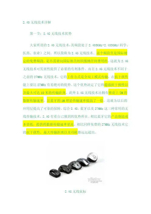
2.4G无线鼠标2.4G无线键鼠套装已经出现有一段时间了,而且一直稳定占据着中低端无线键鼠的市场。
蓝牙目前还是被作为高端无线技术应用在键鼠之上。
市场份额相对较少但是却不可或缺,因为蓝牙有本身相对开放的连接协议。
而不是2.4G无线的通过兑码实现的点对点连接。
不过,因为键鼠的身份比较特殊,一台电脑一套键鼠已经足以应付。
不像PSP或是手机那样本身就是一个载体可以利用蓝牙的点对面功能收发数据,这就决定了2.4G无线技术在键鼠产品上是未来的发展趋势所在。
2.4G无线键盘既然是未来的发展趋势,被用户广泛应用是时间迟早的问题。
讲究便携、抗干扰、以及传输距离的HTPC用户恰好和2.4G无线技术的诸多特点相融合。
如今很多知名的键鼠厂商已经把未来的无线技术产品发展方向对准了2.4G。
有了大的厂商带动,相信越来越多的用户会对2.4G 无线键鼠产品产生浓厚的兴趣。
第二节:2.4G无线键鼠收发模块介绍通过我们一直以来对市场中大部分品牌的资料收集,基本目前市场中的2.4G无线键鼠产品所用到的无线收发模块都是NRF24L01芯片,此款芯片出自挪威著名IC芯片公司Nordic。

2.4G无线双向数据传输模块JF24C资料说明目前2.4G 产品应用比较广泛,有些芯片性能也很不错,但价位都比较偏高,很难进入量产的产品。
为降低成本JF24C模块采用裸片绑定,虽然性能指标略低于目前具有代表性的nRF2401 CC2500 A7105但它的价格要比它们低很多,完全可以满足一般需要双向数据传输及双向遥控的短距离产品应用。
单发单收的产品使用比较简单,加电加信号就发射,收到信号就有输出,纯硬件产品单向传输,不需要软件程序的支持就可以完成收发功能。
2.4G产品就比较复杂化了,芯片内有CPU需要软件程序的支持,必须要有单片机的指令才可以完成双向收发功能。
单发单收的产品成本低廉应用广泛,但存在着严重的无法避免的同频干扰,2.4G产品具有跳频功能一般都有几十至100多个通道可以避开干扰。
但2.4G产品复杂的软件程序也使一些不懂单片机的工程师望而怯步,同时2.4G 产品的功耗及成本还有对墙体的穿透性能下降也影响到在低端产品的普及应用。
JF24C技术规格书测试板演示程序【性能介绍】JF24C无线双向传输模块整合了高頻鍵控(GFSK)收发电路的功能,以特小体积实现高速数据传输的功能。
其中內含先进先出(FIFO)缓冲器,减轻微控制器(microcontroller)在数据处理的负担,实现低成本MCU完成高速数据传输的解決方案与射頻应用的方便性。
同时此模块的传输速率可达到1Mbps,並具有快速跳頻(fast hopping)、向前纠錯(Forward Error Correction)、循环冗余校验(CRC)等功能,可在拥挤的ISM 频段中达到稳定可靠的数据传输。
【主要特点】低电压,高效率低成本,双向高速数据傳輸 特小体积(不需要外接天线) 具有快速跳頻,前向纠錯,校验等功能 工作在全球开放的ISM 频段,免许可证使用。
【性能参数】频率范围:2400-2482Mhz(81信道)工作电压:2.5-3.6VRF 输出功率:10dBm 调制方式:GFSK 发射电流:26mA (TX) 最大速率:1M 接收电流:25mA (RX) 灵敏度:-85dBm 休眠电流:3.5uA最大距离:100米 待机电流:1.9mA (休眠唤醒状态) 编程接口:SPI 数字接口天线形式:PCB 天线模块尺寸:22X12X3mm(长X 宽X 厚)【应用范围】工业数据传输,无线遥控,无线鼠标,无线键盘,无线电子标签,遥控玩具,自动化数据采集系统;工业无线控制;水、气、热、电等居民计量表具无线远传自动抄表。
XN297L 系列产品说明书2.4GHz 单片高速无线收发芯片概述XN297L系列芯片是工作在2.400~2.483GHz世界通用ISM频段的单片无线收发芯片。
该芯片集成射频收发机、频率发生器、晶体振荡器、调制解调器等功能模块,并且支持一对多组网和带ACK的通信模式。
发射输出功率、工作频道以及通信数据率均可配置。
芯片已将多颗外围贴片阻容感器件集成到芯片内部。
主要特性1、功耗较低发射模式(2dBm)工作电流19mA;接收模式工作电流15mA;休眠电流2uA。
2、节省外围器件支持外围5个元器件,包括1颗晶振和4个贴片电容;支持双层或单层印制板设计,可以使用印制板微带天线;芯片自带部分链路层的通信协议;配置少量的参数寄存器,使用方便。
3、性能优异250K / 1M / 2M bps模式的接收灵敏度为-91 / -87 / -83dBm;发射输出功率最大可达13dBm;抗干扰性好,接收滤波器的邻道抑制度高,接收机选择性较好。
其它特性应用方案目录1 命名规则 (4)1.1 XN297L 命名规则 (4)1.2 XN297L 系列产品选择 (4)2 主要电特性 (4)3 极限最大额定值 (3)4 系统结构方框图 (4)5 引脚定义 (5)6 芯片工作状态 (6)6.1 休眠模式 (8)6.2 待机模式-I(STB1) (8)6.3 待机模式-III(STB3) (8)6.4 待机模式-II(STB2) (8)6.5 接收模式 (9)6.6 发射模式 (9)7 数据通信模式 (9)7.1 普通模式 (11)7.2 增强模式 (11)7.3 增强发送模式 (12)7.4 增强接收模式 (12)7.5 增强模式下的数据包识别 (13)7.6 增强模式下的PTX 和PRX 的时序图 (13)7.7 增强模式下的接收端一对多通信 (14)7.8 DATA F I F O (15)7.9 中断引脚 (16)8 SPI 控制接口 (16)8.1 SPI 指令格式 (16)8.2 SPI 时序 (18)9 控制寄存器 (20)10 数据包格式描述 (36)10.1 普通模式的数据包形式 (36)10.2 增强模式的数据包形式 (36)10.3 增强模式的ACK 包形式 (37)11 典型应用电路(参考) (37)12 封装尺寸 (38)13 联系方式 (39)1 命名规则1.1 XN297L 命名规则图1 X N297L系列芯片命名规则1.2 XN297L 系列产品选择表1 XN297L系列产品选择2 主要电特性表2 XN297L系列芯片主要电特性频道的接收灵敏度退化 2dB;发射信号调制精度(EVM)退化10%。
1.引言计的信号范围、音质和最长播放时间方面面临着重大挑战。
为满足这些要求,工程师可以利用来自多家制造商的大量可用产品,包括(按字母顺序)Analog在典型的无线娱乐系统(图1)中,源信号通过带有可选范围扩展器的无线射频接口传输到播放器系统,例如立体声耳机或扬声器。
在播放器内,相应的无线射频接口接收信号以供编解码器、音频处理器或 DSP 处理,以创建驱动到扬声器的最终模拟信号。
一个适当的电源,通常包括一个电池和充电管理电路,完成了系统。
子系统的可用集成解决方案可以帮助工程师满足这些要求,同时降低设计复杂性和成本。
2.频带遗留问题、市场接受度和未授权带宽的可用性通常会推动无线电通信频率的选择。
同时,满足增加操作范围和延长电池寿命的要求为有用频段设置了界限。
对增加功率的需求是对更远距离操作的渴望的自然结果,但射频波长的选择在平衡范围和功率方面起着至关重要的作用。
射频波长和范围之间的关系在Friis 传输方程中进行了描述:其中Pt = 发射功率Pr = 接收功率Gt = 发射器天线增益Gr = 接收器天线增益λ = 波长d = 发射器和接收器之间的距离对于统一参数,距离成为波长的简单线性函数,因此更长波长的无线电通信等同于更大的范围。
当然,更长的波段面临着包括干扰和有效载荷带宽在内的问题。
在这种情况下,2.4 GHz ISM 频段在实际范围限制和有用带宽之间提供了良好的平衡。
2.4 GHz 解决方案的吸引力在于它们能够以低功耗提供有用的有效范围,以及它们的全球可用性。
在蓝牙等标准中使用的基于跳频扩频(FHSS)的2.4 GHz 设计具有在高度活跃的无线电环境中相对不受干扰信号影响的优势。
与较低的ISM 频段相比,这些系统还提供足够的数据带宽,以允许高质量立体声的数字传输,后者通常仅限于模拟或较低数据速率的数字音频。
蓝牙标准工作频率为 2.4 GHz,非常适合消费者的连接要求。
它的广泛使用使得基于蓝牙的无线音频播放器很可能会找到兼容的音频主机,例如计算机、笔记本电脑、平板电脑和智能手机。
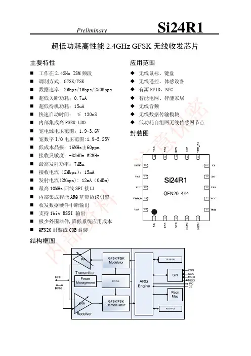
PL1167单片低功耗高性能 2.4GHz无线射频收发芯片芯片概述:主要特点:PL1167是一款工作在 2.4~2.5GHz 世界通用 ISM频段的单片低功耗高性能 2.4GHz无线射频收发芯片。
ψ 低功耗高性能2.4GHz无线射频收发芯片ψ 无线速率:1Mbps 该单芯片无线收发器集成包括:频率综合器、功率放大器、晶体振荡器、调制解调器等模块。
ψ 内置硬件链路层ψ 内置接收强度检测电路输出功率、信道选择与协议等可以通过 SPI或 I2C接ψ 支持自动应答及自动重发功能ψ 内置地址及FEC、CRC校验功能ψ 极短的信道切换时间,可用于跳频ψ 使用微带线电感和双层PCB板ψ 低工作电压:1.9~3.6V口进行灵活配置。
支持跳频以及接收强度检测等功能,抗干扰性能强,可以适应各种复杂的环境并达到优异的性能。
内置地址及 FEC、CRC校验功能。
ψ 封装形式:QFN16/TSSOP16 内置自动应答及自动重发功能。
ψψQFN16仅支持SPI接口芯片发射功率最大可以达到 5.5dBm,接收灵敏度可以达到-88dBm。
TSSOP16可支持SPI与I2C接口内置电源管理功能,掉电模式和待机模式下待机电流可以减小到接近 1uA。
应用:ψ 无线鼠标,键盘,游戏机操纵杆ψ 无线数据通讯ψ 无线门禁管脚分布图:ψ 无线组网ψ 安防系统ψ 遥控装置ψ 遥感勘测ψ 智能运动设备ψ 智能家居ψ 工业传感器ψ 工业和商用近距离通信ψ IP电话,无绳电话ψ 玩具1概要性能强,可以适应各种复杂的环境并达到优异的 性能。
PL1167 是一款工作在 2.4~2.5GHz 世界通 用 ISM 频段的单片低功耗高性能 2.4GHz 无线射 频收发芯片。
内置地址及 FEC 、CRC 校验功能。
该单芯片无线收发器集成包括:频率综合器、 功率放大器、晶体振荡器、调制解调器等模块。
内置自动应答及自动重发功能。
芯片发射功率最大可以达到 5.5dBm ,接收 灵敏度可以达到-88dBm 。
输出功率、信道选择与协议等可以通过 SPI 或 I2C 接口进行灵活配置。
内置电源管理功能,掉电模式和待机模式下 待机电流可以减小到接近 1uA 。
支持跳频以及接收强度检测等功能,抗干扰2特性ζ 低功耗高性能2.4GHz 无线射频收发芯片 ζ 无线速率:1Mbps ζ 极短的信道切换时间,可用于跳频 ζ 使用微带线电感和双层PCB 板 ζ 低工作电压:1.9~3.6V ζ 内置硬件链路层 ζ 内置接收强度检测电路ζ 封装形式:QFN16/TSSOP16 ζ 支持自动应答及自动重发功能 ζ 内置地址及FEC 、CRC 校验功能ζ ζQFN16仅支持SPI 接口 TSSOP16可支持SPI 与I2C 接口3快速参考数据参数数值单位最低工作电压 最大发射功率 数据传输速率 发射模式功耗@0dBm 接收模式功耗 工作温度范围 接收灵敏度 1.9 V dBm Mbps mA 5.5 1 16 17 -40 to +85-88 mA ℃ dBm uA掉电模式功耗14管脚分布图QFN16 管脚分布图如下:说明:MODE管脚在芯片内连接到VSS,因此QFN16仅支持SPI接口。
TSSOP16 管脚分布图如下:5管脚描述Pin(QFN16) 管脚名类型描述1 ANTBANT 天线天线接口2 天线天线接口3,8,17 VSS 电源接地(0V)4,5 6 N/C 悬空悬空不接PKT 数字输出数字输入数字输入发射/接收包状态指示位复位脚,低电平有效7 RSTBSCSB9 SPI接口从模式使能信号,低电平有效从SLEEP模式唤醒芯片10111213141516 SCKSDI数字输入数字输入数字输出电源SPI接口时钟输入SPI接口数据输入SPI接口数据输出(无效时为三态)电源(3.3V)SDOVCCVDDOXOUTXIN电源 1.8V内部LDO输出,外接电容晶振输出模拟输出模拟输入晶振输入Pin(TSSOP16) 管脚名类型描述1 2 3 4 5 6 AVSSN/C电源接地(0V)悬空悬空不接PKT 数字输出数字输入发射/接收包状态指示位复位脚,低电平有效接地(0V)RSTBDVSSSCSB电源数字输入SPI:SPI接口从模式使能信号,低电平有效从SLEEP模式唤醒芯片I2C:从SLEEP模式唤醒芯片SCK:SPI接口时钟输入7 8 9 SCK/SCL 数字输入SCL:I2C接口时钟输入SDI/A4 数字输入SDI:SPI接口数据输入A4:I2C接口地址位4SDO/SDA 数字输出数字I/OSDO:SPI接口数据输出(无效时为三态)SDA:I2C接口数据输入输出I/O接口模式选择:10 MODE 数字输入Pin(TSSOP16) 管脚名类型描述VSS :选择SPI 接口 VCC :选择I2C 接口11 12 13 14 15 16VCC 电源 电源(3.3V)VDDO XOUT XIN 电源 1.8V 内部LDO 输出,外接电容 晶振输出 模拟输出 模拟输入 天线 晶振输入 ANTB ANT天线接口 天线天线接口6结构框图7最大额定值参数符号范围单位VCC 供电电压VCC-0.3 to +3.6V参数符号VDDO V IN 范围单位V VDDO 供电电压 输入电压 输出电压 工作温度 仓储温度-0.3 to +2.5 -0.3 to (VCC+0.3) -0.3 to (VCC+0.3)-40 to +85 V V OUT T OP ℃ ℃T ST-40 to +125注释:超过最大额定值可能损毁器件;超过推荐工作范围的芯片功能特性不能保证;长时间工作于 最大额定条件下可能会影响器件的稳定性。
8电气特性(VCC=+3V ,VSS=0V ,TA=-40℃ to +85℃)符号参数(条件)说明 最小值 典型 最大值 单位工作条件 VCC T OPVCC 供电电压 1.9 -403.33.6 85V 工作温度 ℃数字输入管脚V IH V IL高电平输入电压 低电平输入电压 0.8VCC 0 1.2VCC 0.2VCC V V数字输出管脚V OH V OL高电平输出电压 低电平输出电压 0.8VCC 0VCC V V0.2VCC 常规射频条件f OP 工作频段 24002482MHz MHz KHz f XTAL 晶振频率12 △f 1M R GFSK F CHANNEL频率偏移@1Mbps 数据传输速率 信道间隔 280 1 Mbps MHz1 发射操作P RF 最大输出功率 05.5 22 dBm dB P RFC P RF1 P RF2 I VCC_H I VCC_L射频功率控制范围 第一临近信道发射功率 第二临近信道发射功率 高增益时功耗 1820-20 -50dBm dBm mA 16 12低增益时功耗 mA 接收操作 I VCC 接收功耗17 mA RX SENS0.1% BER 时接收灵敏度-88dBm9 SPI 接口9.1 SPI 接口说明PL1167收发芯片提供简单的 MCU 接口 SPI 模式,芯片的 SPI 接口只支持从模式。
SPI 接口包含 7个相关信号,如下表:管脚描述RSTB MODE SCSB 复位脚,低电平有效模式选择,为 0时选择 SPI 模式 SPI 接口从模式使能信号,低电平有效 从SLEEP 模式唤醒芯片 SPI 接口时钟输入 SCK SDI SPI 接口数据输入 SDO PKTSPI 接口数据输出 发射/接收包状态指示位9.2 SPI 命令格式符号最小 典型 最大 描述T SSH250ns两次 SPI 命令时间间隔符号最小典型最大描述T ,T SSR 41.5ns*1 SCSB与 SCK时间间隔SSFT A2D T H2L T R2R T SCK地址与数据时间间隔高低字节数据时间间隔两个寄存器数据时间间隔SCK时钟周期*1*183ns注:*1—在读 FIFO数据时,至少需要 450ns等待时间;其它寄存器时 T3min = 41.5ns。
10 I2C接口10.1 I2C接口说明管脚RSTB MODE SCSB SCL 描述复位脚,低电平有效模式选择,为 1时选择 I2C模式从 SLEEP模式唤醒芯片I2C接口时钟输入I2C数据输入输出 I/OI2C接口地址位 4SDAA410.2 I2C支持特性I2C从模式选择支持与否标准模式– 100 kbps快速模式– 400 kbps增强型快速模式– 1000 kbps 高速模式– 3200 kbps时钟展宽是是是否否否否否否10位从地址广呼方式地址软件复位器件 ID10.3 I2C命令格式10.4 I2C器件地址A6 A5 A4 A3 A2 A1 A0 R/W0 1 A4 Pin 1 0 0 0 Read=1Write=011控制寄存器最新的推荐控制寄存器值参考《用户手册》,请联系供应商索取。
12典型应用13封装QFN16 封装QFN16(4x4mm, 0.65mm pitch, Thinner) 封装尺寸TSSOP16 封装TSSOP16封装尺寸14注意事项为了持续改进产品的可靠性、功能或设计,保留随时更新修改的权利,并不另行通知客户。
客户在下单前请确认所使用的是最新的完整版说明书。