XH7145A售前资料
- 格式:doc
- 大小:125.50 KB
- 文档页数:4
Q/SSJ 300.3-GS10 XK714B型数控床身铣床使用说明书(电气分册)14.0912.060工作台面宽度 400mm工作台面长度 1000mm出 厂 编 号中 华 人 民 共 和 国上 海 第 三 机 床 厂Q/SSJ 300.3-GS11上海第三机床厂使用说明书 14.0912.060编制标准化审批日期注 意 事 项1 开箱验收用户开箱验收时,如发现产品及附件与装箱单不符,请及时与制造厂经销部门联系。
2 安装使用安装使用产品前,必须仔细阅读说明书!3 输入电源要求a)电源电压为0.9~1.1倍额定电压。
b)频率为0.99~1.01倍额定频率(连续工作)。
频率为0.98~1.02倍额定频率(短时工作)。
4 机床安全防护和报警等安全措施,尤须注意。
本文件版本号: 2005 年 9 月安全说明1.首先感谢贵公司选用我厂设备。
但在使用本机床前,请详细阅读本说明书及SINUMERIK802DSL系统操作说明书。
2.请操作者注意,不适当的操作有可能造成人员或设备损害。
2.1请定期检查超程开关,紧停按钮等器件的有效性,以保证机床的紧急停止功能始终处于正常状态。
定期检查机床接地是否与工厂接地的牢固可靠。
2.2只关闭CNC的电源,动力电源仍向有些部位供电,即使关闭机床总电源,机床照明电仍有电,必须给予注意。
2.3关闭电源后,伺服放大器、变频器内的电压仍会保留一段时间,不适当的维修行为,存在被电击的危险。
2.4用户的衣物可能会卷进机床主轴或其它部件中,因此造成伤害。
2.5需打开电箱门检查时,先断开机床总电源开关,然后才能开电箱门。
带电操作检查要注意强电部分,触碰端子存在被电击的严重危险。
2.6 系统单元内部、伺服单元内部均存在高压电路,用户不要拆卸,即使专业人员也要格外小心。
3.该机床的维修应请专业人员或经过授权的其他人员进行,采用不正确的维修手段,很可能造成机床新的故障产生。
保修期内机床出现重大故障请及时与我厂联系。
数控加工中心机床XH714的操作一、主要用途和特性XH714立式加工中心是一种中小规格、高效通用的自动化机床。
该机床设有可容20把刀具的自动换刀系统,并有先进的数字控制系统Sinumerik810D,通过编程,在一次装夹中可自动完成铣、镗、钻、铰、攻丝等多种工序的加工。
若选用数控转台,可扩大为四轴控制,实现多面加工。
XH714立式加工中心采用稠筋封闭式框架结构,刚性高、抗震性好;主传动采用交流调速电机,在45~450rpm范围内无级变速,对不同零件加工的适应力强。
三向采用镶钢——贴塑导轨副,滚珠丝杠传动,高速进给震动小,低速无爬行,精度稳定性高;间隙自动润滑系统使各主要运动部件均能得到良好的自动润滑,有效地提高了可靠性和使用寿命,因此,该机床具有刚性好、变速范围宽、精度高、柔性大等特点,特别适用于多品种生产的机器制造厂。
二、主要规格参数1.主轴主轴孔锥度ISO 40#(7:24)主轴转数(电机无级调速)45~4500 rpm2.工作台工作台面积(宽×长)400×1150mmT型槽数及宽度3×18H8 mmT型槽间距125 mm工作台允许最大承重500kg3.行程工作台纵向行程(X轴)720 mm工作台横向行程(Y轴)400 mm垂向行程(Z轴)500 mm主轴端面至工作台面距离125~625 mm主轴中心至立柱导轨面距离450 mm工作台中心至立柱导轨面距离245~645 mm4.进给速度进给速度范围1~5000mm/min快速移动速度10m/min三向滚珠丝杠直径ф40 mm5.刀库刀库容量20把换刀时间7秒6.精度分辩率0.001mm定位精度X轴0.040 mm定位精度Y、Z轴0.030 mm重复定位精度0.016 mm7.控制系统控制系统型号Sinumerik810D系统分辩率0.001mm或0.0001 inch主要参数见Sinumerik 810D系统介绍8.电机容量主轴电机5.5/7.5kw进给电机X、Y向0.9 kw进给电机Z向1.8 kw刀库电机30 kw冷泵电机125 kw润滑电机3 kw机床电源380V50Hz9.外形尺寸2300×2300×2500 mm10.机床重量4500 kg三、机床主要结构及工作原理本机床由床身部件、立柱部件、铣头部件、工作台床鞍部件、刀库部件、润滑系统、冷却系统、气动系统、电气系统等部分组成。

第一节数控加工中心机床XH714的操作4.1.1主要用途和特性XH714立式加工中心是一种中小规格、高效通用的自动化机床。
该机床设有可容20把刀具的自动换刀系统,并有先进的数字控制系统Sinumerik810D,通过编程,在一次装夹中可自动完成铣、镗、钻、铰、攻丝等多种工序的加工。
若选用数控转台,可扩大为四轴控制,实现多面加工。
XH714立式加工中心采用稠筋封闭式框架结构,刚性高、抗震性好;主传动采用交流调速电机,在45~450rpm范围内无级变速,对不同零件加工的适应力强。
三向采用镶钢——贴塑导轨副,滚珠丝杠传动,高速进给震动小,低速无爬行,精度稳定性高;间隙自动润滑系统使各主要运动部件均能得到良好的自动润滑,有效地提高了可靠性和使用寿命,因此,该机床具有刚性好、变速范围宽、精度高、柔性大等特点,特别适用于多品种生产的机器制造厂。
4.1.2主要规格参数1.主轴主轴孔锥度ISO 40#(7:24)主轴转数(电机无级调速)45~4500 rpm2.工作台工作台面积(宽×长)400×1150mmT型槽数及宽度3×18H8 mmT型槽间距125 mm工作台允许最大承重500kg3.行程工作台纵向行程(X轴)720 mm工作台横向行程(Y轴)400 mm垂向行程(Z轴)500 mm主轴端面至工作台面距离125~625 mm主轴中心至立柱导轨面距离450 mm工作台中心至立柱导轨面距离245~645 mm 4.进给速度进给速度范围1~5000mm/min快速移动速度10m/min三向滚珠丝杠直径ф40 mm5.刀库刀库容量20把换刀时间7秒6.精度分辩率0.001mm定位精度X轴0.040 mm定位精度Y、Z轴0.030 mm重复定位精度0.016 mm7.控制系统控制系统型号Sinumerik810D系统分辩率0.001mm或0.0001 inch主要参数见Sinumerik 810D系统介绍8.电机容量主轴电机5.5/7.5kw进给电机X、Y向0.9 kw进给电机Z向1.8 kw刀库电机30 kw冷泵电机125 kw润滑电机3 kw机床电源380V50Hz9.外形尺寸2300×2300×2500 mm10.机床重量4500 kg4.1.3机床主要结构及工作原理本机床由床身部件、立柱部件、铣头部件、工作台床鞍部件、刀库部件、润滑系统、冷却系统、气动系统、电气系统等部分组成。
XKA714C型数控铣床技术协议甲方:天水风动机械有限责任公司乙方:北京北一数控机床有限责任公司一、概述XKA714C型是使用范围很广的铣床,主轴前锥孔为国际标准(ISO)No.50,可安装各种圆柱铣刀、圆片铣刀、角度铣刀、端面铣刀等刀具,还可借助弹簧夹头安装小规格直柄铣刀。
它的横向(Y向)移动由底座上的滑座来完成,滑座上的工作台可纵向(X向)移动,立柱上的主轴箱可进行垂向(Z向)移动。
工作台、滑座、主轴箱的移动共同组成了机床X、Y、Z三个轴线方向的运动。
本机床与同类产品相比,具有承载能力大,主轴扭矩大420NM等特点。
机床采用FANUC数控系统,可以完成直线铣削,组成各种往复循环、框式循环;能实现三坐标联动加工,可进行直线插补、圆弧插补;适用于铣削具有复杂曲线轮廓及截面的零件,如凸轮、样板、叶片、弧形槽等零件,适用于各行业的机械零件加工。
本机床符合JB/T8329·1-1999《数控床身铣床精度检验》和Q/B121·474-1995《数控铣床位置精度》的标准;出厂验收文件为机床《合格证明书》。
二、机床传动系统主传动系统由7.5KW的交流变频电机驱动,电机安装在主轴箱的顶面,经高速档齿轮使主轴获得200~3200r/min的高速档无级变速段。
另外通过油缸中的活塞带动拨叉推动滑移齿轮来完成高速档和低速档的变换,再通过齿轮降速组,使主轴获得的50~800r/min低速档无级变速段。
主轴内装有拉刀机构,拉刀机构采用液压装置及蝶形弹簧来完成松刀、拉刀动作。
进给传动系统中X向、Y向坐标由交流伺服电机通过1∶1.5同步齿形带驱动滚珠丝杠,分别拖动工作台和滑座进行X向、Y向运动,使工作台获得6~3200mm/min的切削进给速度及8000mm/min的快速移动速度。
Z向进给由交流伺服电机通过一对24∶54的齿轮降速,将动力传给Z向滚珠丝杠,拖动主轴箱运动,使主轴箱获得3~1600mm/min的切削进给速度及4000mm/min的快速移动速度。

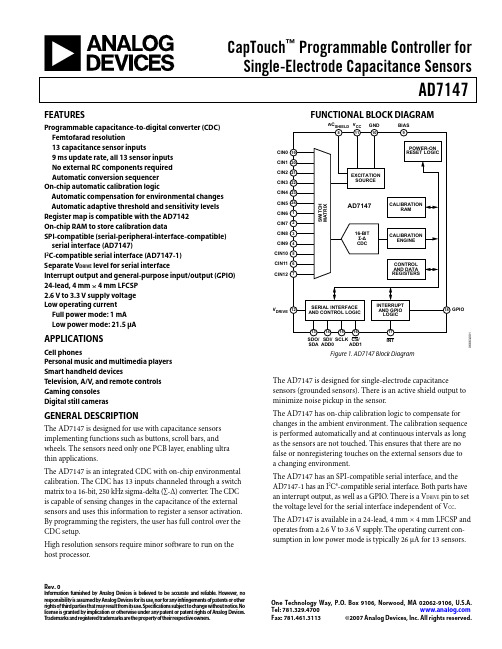
CapTouch™ Programmable Controller forSingle-Electrode Capacitance SensorsAD7147 Rev. 0Information furnished by Analog Devices is believed to be accurate and reliable. However, noresponsibility is assumed by Analog Devices for its use, nor for any infringements of patents or other rights of third parties that may result from its use. Specifications subject to change without notice. No license is granted by implication or otherwise under any patent or patent rights of Analog Devices. T rademarks and registered trademarks are the property of their respective owners. One Technology Way, P.O. Box 9106, N orwood, MA 02062-9106, U.S.A. Tel: 781.329.4700 Fax: 781.461.3113 ©2007 Analog Devices, Inc. All rights reserved.FEATURESProgrammable capacitance-to-digital converter (CDC) Femtofarad resolution13 capacitance sensor inputs9 ms update rate, all 13 sensor inputsNo external RC components requiredAutomatic conversion sequencerOn-chip automatic calibration logicAutomatic compensation for environmental changes Automatic adaptive threshold and sensitivity levels Register map is compatible with the AD7142On-chip RAM to store calibration dataSPI-compatible (serial-peripheral-interface-compatible) serial interface (AD7147)I2C-compatible serial interface (AD7147-1)Separate V DRIVE level for serial interfaceInterrupt output and general-purpose input/output (GPIO) 24-lead, 4 mm × 4 mm LFCSP2.6 V to3.3 V supply voltageLow operating currentFull power mode: 1 mALow power mode: 21.5 μAAPPLICATIONSCell phonesPersonal music and multimedia playersSmart handheld devicesTelevision, A/V, and remote controlsGaming consolesDigital still camerasGENERAL DESCRIPTIONThe AD7147 is designed for use with capacitance sensors implementing functions such as buttons, scroll bars, and wheels. The sensors need only one PCB layer, enabling ultra thin applications.The AD7147 is an integrated CDC with on-chip environmental calibration. The CDC has 13 inputs channeled through a switch matrix to a 16-bit, 250 kHz sigma-delta (∑-Δ) converter. The CDC is capable of sensing changes in the capacitance of the external sensors and uses this information to register a sensor activation. By programming the registers, the user has full control over the CDC setup.High resolution sensors require minor software to run on the host processor.FUNCTIONAL BLOCK DIAGRAMCIN0CIN1CIN2CIN3CIN4CIN5CIN6CIN7CIN8CIN9CIN10CIN11CIN12V DRIVE GPIOSDA ADD0ADD16663-1Figure 1. AD7147 Block DiagramThe AD7147 is designed for single-electrode capacitance sensors (grounded sensors). There is an active shield output to minimize noise pickup in the sensor.The AD7147 has on-chip calibration logic to compensate for changes in the ambient environment. The calibration sequence is performed automatically and at continuous intervals as long as the sensors are not touched. This ensures that there are no false or nonregistering touches on the external sensors due to a changing environment.The AD7147 has an SPI-compatible serial interface, and the AD7147-1 has an I2C®-compatible serial interface. Both parts have an interrupt output, as well as a GPIO. There is a V DRIVE pin to set the voltage level for the serial interface independent of V CC. The AD7147 is available in a 24-lead, 4 mm × 4 mm LFCSP and operates from a 2.6 V to 3.6 V supply. The operating current con-sumption in low power mode is typically 26 μA for 13 sensors.AD7147Rev. 0 | Page 2 of 68TABLE OF CONTENTSFeatures..............................................................................................1 Applications.......................................................................................1 General description..........................................................................1 Functional Block Diagram..............................................................1 Revision History...............................................................................2 Specifications.....................................................................................3 SPI Timing Specifications (AD7147).........................................5 I 2C Timing Specifications (AD7147-1).....................................6 Absolute Maximum Ratings............................................................7 ESD Caution..................................................................................7 Pin Configurations and Function Descriptions...........................8 Typical Performance Characteristics.............................................9 Theory of Operation......................................................................11 Capacitance-Sensing Theory....................................................11 BIAS Pin.......................................................................................12 Operating Modes........................................................................12 Capacitiance-to-Digital Converter...............................................14 Oversampling the CDC Output...............................................14 Capacitance Sensor Offset Control..........................................14 Conversion Sequencer...............................................................14 CDC Conversion Sequence Time............................................16 CDC Conversion Results...........................................................16 Capacitance Sensor Input Configuration....................................17 CINx Input Multiplexer Setup..................................................17 Single-Ended Connections to the CDC..................................17 Noncontact Proximity Detection.................................................18 Recalibration...............................................................................18 Proximity Sensitivity..................................................................18 FF_SKIP_CNT. (21)Environmental Calibration...........................................................23 Capacitance Sensor Behavior Without Calibration...............23 Capacitance Sensor Behavior with Calibration......................24 Slow FIFO....................................................................................24 SLOW_FILTER_UPDATE_LVL..............................................24 Adaptive Threshold and Sensitivity.............................................25 Interrupt Output.............................................................................27 CDC Conversion-Complete Interrupt....................................27 Sensor-Touch Interrupt.............................................................27 GPIO INT Output Control.......................................................29 Outputs............................................................................................31 AC SHIELD Output..........................................................................31 GPIO............................................................................................31 Using the GPIO to Turn On/Off an LED................................31 Serial Interface................................................................................32 SPI Interface................................................................................32 I 2C-Compatible Interface..........................................................34 V DRIVE Input.................................................................................36 PCB Design Guidelines.................................................................37 Capacitive Sensor Board Mechanical Specifications.............37 Chip Scale Packages...................................................................37 Power-Up Sequence.......................................................................38 Typical Application Circuits.........................................................39 Register Map...................................................................................40 Detailed Register Descriptions.....................................................41 Bank 1 Registers.........................................................................41 Bank 2 Registers.........................................................................51 Bank 3 Registers.........................................................................56 Outline Dimensions.......................................................................68 Ordering Guide.. (68)REVISION HISTORY09/07—Revision 0: Initial VersionAD7147SPECIFICATIONSV CC = 2.6 V to 3.6 V, T A = −40o C to +85°C, unless otherwise noted.Rev. 0 | Page 3 of 68AD7147Rev. 0 | Page 4 of 68Table 2. Typical Average Current in Low Power Mode 1Current Values of Conversion Stages (μA)Low Power Mode Delay Decimation Rate 1 2 3 4 5 6 7 8 9 10 11 12 200 ms 64 20.83 24.18 27.52 30.82 34.11 37.37 40.6 43.81 46.99 50.16 53.3 56.41 128 25.3 31.92 38.45 44.87 51.21 57.45 63.6 69.66 75.63 81.52 87.33 93.05256 34.11 46.99 59.51 71.66 83.47 94.94 106.1 116.96 127.52 137.81 147.82 157.58 400 ms 64 18.17 19.86 21.55 23.23 24.9 26.57 28.23 29.88 31.53 33.17 34.81 36.44 128 20.43 23.79 27.12 30.43 33.72 36.98 40.22 43.43 46.62 49.78 52.93 56.05 256 24.9 31.53 38.06 44.5 50.83 57.08 63.23 69.3 75.28 81.17 86.98 92.71 600 ms 64 17.28 18.41 19.54 20.67 21.79 22.91 24.03 25.14 26.25 27.36 28.47 29.57 128 18.79 21.04 23.28 25.51 27.73 29.94 32.13 34.32 36.49 38.65 40.81 42.95 256 21.79 26.25 30.67 35.04 39.37 43.66 47.9 52.11 56.27 60.39 64.47 68.51 800 ms 64 16.84 17.69 18.53 19.38 20.23 21.07 21.91 22.75 23.59 24.43 25.26 26.09 128 17.97 19.66 21.35 23.03 24.7 26.37 28.03 29.69 31.34 32.98 34.62 36.2525620.23 23.59 26.93 30.24 33.53 36.79 40.03 43.24 46.43 49.6 52.74 55.861V CC = 3.3 V, T = 25°C, load = 5 pF.Table 3. Maximum Average Current in Low Power Mode 1Current Values of Conversion Stages (μA)Low Power Mode Delay Decimation Rate 1 2 3 4 5 6 7 8 9 10 11 12 200 ms 64 27.71 31.65 35.56 39.44 43.28 47.1 50.89 54.64 58.37 62.07 65.74 69.38 128 32.96 40.72 48.37 55.89 63.3 70.59 77.77 84.84 91.8 98.66 105.41 112.07256 43.28 58.37 72.99 87.17 100.92 114.26 127.22 139.8 152.03 163.92 175.48 186.73 400 ms 64 24.61 26.6 28.58 30.55 32.51 34.47 36.42 38.36 40.29 42.21 44.13 46.04 128 27.26 31.21 35.12 39 42.85 46.67 50.46 54.22 57.95 61.65 65.33 68.97 256 32.51 40.29 47.94 55.47 62.88 70.18 77.36 84.44 91.41 98.27 105.03 111.69 600 ms 64 23.58 24.91 26.23 27.55 28.87 30.18 31.5 32.8 34.11 35.41 36.7 38 128 25.35 27.99 30.62 33.24 35.84 38.43 41 43.56 46.11 48.64 51.16 53.66 256 28.87 34.11 39.29 44.41 49.48 54.5 59.46 64.38 69.24 74.05 78.81 83.53 800 ms 64 23.06 24.06 25.05 26.05 27.04 28.03 29.02 30 30.98 31.97 32.95 33.92 128 24.39 26.38 28.36 30.33 32.29 34.25 36.2 38.14 40.07 42 43.91 45.8225627.04 30.98 34.9 38.78 42.64 46.46 50.25 54.01 57.74 61.45 65.12 68.771V CC = 3.6 V, T A = −40o C to +85°C, load = 5 pF.AD7147Rev. 0 | Page 5 of 68SPI TIMING SPECIFICATIONS (AD7147)T A = −40°C to +85°C, V DRIVE = 1.65 V to 3.6 V , and V CC = 2.6 V to 3.6 V , unless otherwise noted. Sample tested at 25°C to ensure compliance. All input signals are specified with t R = t F = 5 ns (10% to 90% of V CC ) and timed from a voltage level of 1.6 V .CSSCLKSDISDO06663-002Figure 2. SPI Detailed Timing DiagramAD7147Rev. 0 | Page 6 of 68I 2C TIMING SPECIFICATIONS (AD7147-1)T A = −40°C to +85°C, V DRIVE = 1.65 V to 3.6 V , and V CC = 2.6 V to 3.6 V , unless otherwise noted. Sample tested at 25°C to ensure compliance. All input signals timed from a voltage level of 1.6 V . Table 5. I 2C Timing Specifications 1Parameter Limit Unit Description f SCLK 400 kHz maxt 10.6 μs min Start condition hold time, t HD; STA t 2 1.3 μs min Clock low period, t LOW t 30.6 μs min Clock high period, t HIGH t 4100 ns min Data setup time, t SU; DAT t 5300 ns min Data hold time, t HD; DATt 60.6 μs min Stop condition setup time, t SU; STO t 70.6 μs min Start condition setup time, t SU; STAt 8 1.3 μs min Bus-free time between stop and start conditions, tBUF t R 300 ns max Clock/data rise time t F300 ns max Clock/data fall time1Guaranteed by design, not production tested.SCLKSDA06663-003Figure 3. I 2C Detailed Timing DiagramAD7147Rev. 0 | Page 7 of 68ABSOLUTE MAXIMUM RATINGSTable 6.Parameter RatingV CC to GND −0.3 V to +3.6 VAnalog Input Voltage to GND −0.3 V to V CC + 0.3 VDigital Input Voltage to GND −0.3 V to V DRIVE + 0.3 VDigital Output Voltage to GND −0.3 V to V DRIVE + 0.3 VInput Current to Any Pin Except Supplies 110 mAESD Rating (Human Body Model) 2.5 kV Operating Temperature Range −40°C to +105°C Storage Temperature Range −65°C to +150°C Junction Temperature 150°CLFCSP Power Dissipation 450 mW θJA Thermal Impedance 135.7°C/WIR Reflow Peak Temperature 260°C (±0.5°C) Lead Temperature (Soldering 10 sec) 300°C1Transient currents of up to 100 mA do not cause SCR latch-up.Stresses above those listed under Absolute Maximum Ratingsmay cause permanent damage to the device. This is a stressrating only; functional operation of the device at these or anyother conditions above those indicated in the operationalsection of this specification is not implied. Exposure to absolutemaximum rating conditions for extended periods may affectdevice reliability.PIN06663-004Figure 4. Load Circuit for Digital Output Timing Specifications ESD CAUTIONAD7147Rev. 0 | Page 8 of 68PIN CONFIGURATIONS AND FUNCTION DESCRIPTIONS1CIN62CIN73CIN84CIN95CIN106CIN1115SCLK 1617INT 18GPIO 14SDI 13SDO7C I N 128A C S H I E L D 9B I A S 11V C C 12V D R I V E10G N D 1C I N 22C I N 33C I N 44C I N 50C I N 19C I N 006663-005Figure 5. AD7147 Pin Configuration 1CIN62CIN73CIN84CIN95CIN106CIN11SCLK ADD1GPIO ADD0SDA7C I N 128A C S H I E L D 9B I A S 11V C C 12V D R I V E10G N D 1C I N 22C I N 33C I N 44C I N 50C I N 19C I N 006663-006Figure 6. AD7147-1 Pin ConfigurationIIAD7147Rev. 0 | Page 9 of 68TYPICAL PERFORMANCE CHARACTERISTICS9357952.63.706663-007V CC (V)I C C (µA )915895875855835815 2.7 2.8 2.9 3.0 3.1 3.2 3.3 3.4 3.5 3.6Figure 7. Supply Current vs. Supply Voltage18002.53.706663-061V CC (V)I C C (μA )16014012010080604020 2.7 2.9 3.1 3.3 3.5Figure 8. Low Power Supply Current vs. Supply Voltage,Decimation Rate = 2560.122.53.706663-009V CC (V)I C C (m A )0.100.080.060.040.022.7 2.93.1 3.3 3.5Figure 9. Low Power Supply Current vs. Supply Voltage,Decimation Rate = 12870006663-060V CC (V)I C C (μA )6050403020102.53.72.7 2.93.13.3 3.5Figure 10. Low Power Supply Current vs. Supply Voltage,Decimation Rate = 642.502.706663-010V CC (V)I C C (µA )2.01.51.00.52.8 2.93.0 3.1 3.2 3.3 3.4 3.5 3.6Figure 11. Shutdown Supply Current vs. Supply Voltage1150900006663-062AC SHIELD CAPACITIVE LOAD (pF)I C C (µA )110010501000950100200300400500Figure 12. Supply Current vs. Capacitive Load on AC SHIELDAD7147Rev. 0 | Page 10 of 685800040000006663-063AC SHIELD CAPACITIVE LOAD (pF)C D C C O D E(d )1002003004005005600054000520005000048000460004400042000Figure 13. Output Code vs. Capacitive Load on AC SHIELD 960780–60–40–2002040608010012006663-013TEMPERATURE (°C)I C C (µA )940920900880860840820800Figure 14. Supply Current vs. Temperature120–4513506663-014TEMPERATURE (°C)I C C (µA )108642–25–51535557595115Figure 15. Shutdown Supply Current vs. Temperature16002550100200400800160032006400128002560051200102400204800409600819200164000006663-064SINE WAVE FREQUENCY (Hz)C D C N O I S E p -p (L S B )140120*********20Figure 16. Power Supply Sine Wave Rejection, V CC = 3.6 V1202550100200400800160032006400128002560051200102400204800409600819200164000006663-065SQUARE WAVE FREQUENCY (Hz)C D C N O I S E p -p (L S B)10080604020Figure 17. Power Supply Square Wave Rejection, V CC = 3.6 V350010000200003000040000500006000006663-016CDC OUTPUT CODEI N P U T C AP A C I T A N C E (p F )30252015105Figure 18. CDC Linearity, V CC = 3.3 VTHEORY OF OPERATIONThe AD7147 and AD7147-1 are CDCs with on-chip environmental compensation. They are intended for use in portable systems requiring high resolution user input. The internal circuitry consists of a 16-bit, ∑-Δ converter that can change a capacitive input signal into a digital value. There are 13 input pins, CIN0 to CIN12, on the AD7147 or AD7147-1. A switch matrix routes the input signals to the CDC. The result of each capacitance-to-digital conversion is stored in on-chip registers. The host subsequently reads the results over the serial interface. The AD7147 has an SPI interface, and the AD7147-1 has an I2C interface, ensuring that the parts are compatible with a wide range of host processors. AD7147 refers to both theAD7147 and AD7147-1, unless otherwise noted, from this point forward in this data sheet.The AD7147 interfaces with up to 13 external capacitance sensors. These sensors can be arranged as buttons, scroll bars, or wheels, or as a combination of sensor types. The external sensors consist of an electrode on a single- or multiple-layer PCB that interfaces directly to the AD7147.The AD7147 can be set up to implement any set of input sensors by programming the on-chip registers. The registers can also be programmed to control features such as averaging, offsets, and gains for each of the external sensors. There is an on-chip sequencer that controls how each of the capacitance inputs is polled.The AD7147 has on-chip digital logic and 528 words of RAM that are used for environmental compensation. The effects of humidity, temperature, and other environmental factors can affect the operation of capacitance sensors. Transparent to the user, the AD7147 performs continuous calibration to compen-sate for these effects, allowing the AD7147 to consistently provide error-free results.The AD7147 requires a companion algorithm that runs on the host or another microcontroller to implement high resolution sensor functions, such as scroll bars or wheels. However, no companion algorithm is required to implement buttons. Button sensors are implemented on chip, entirely in digital logic.The AD7147 can be programmed to operate in either full power mode or low power automatic wake-up mode. The automatic wake-up mode is particularly suited for portable devices that require low power operation to provide the user with significant power savings and full functionality.The AD7147 has an interrupt output, INT, to indicate when new data has been placed into the registers. INT is used to interrupt the host on sensor activation. The AD7147 operates from a 2.6 V to 3.6 V supply and is available in a 24-lead, 4 mm × 4 mm LFCSP.CAPACITANCE-SENSING THEORYThe AD7147 measures capacitance changes from single-electrode sensors. The sensor electrode on the PCB comprises one plate of a virtual capacitor. The other plate of the capacitor is the user’s finger, which is grounded with respect to the sensor input.The AD7147 first outputs an excitation signal to charge the plate of the capacitor. When the user comes close to the sensor, the virtual capacitor is formed, with the user acting as the second capacitor plate.6663-17Figure 19. Capacitance-Sensing MethodA square wave excitation signal is applied to CINx during the conversion, and the modulator continuously samples the charge going through CINx. The output of the modulator is processed via a digital filter, and the resulting digital data is stored in the CDC_RESULT_Sx registers for each conversion stage, at Address 0x00B to Address 0x016.Registering a Sensor ActivationWhen a user approaches a sensor, the total capacitance associated with that sensor changes and is measured by the AD7147. If the change causes a set threshold to be exceeded, the AD7147 interprets this as a sensor activation.On-chip threshold limits are used to determine when a sensor activation occurs. Figure 20 shows the change in CDC_RESULT_Sx when a user activates a sensor. The sensor is deemed to be active only when the value of CDC_RESULT_Sx is either greater than the value of STAGEx_HIGH_THRESHOLD or less than the value of STAGEx_LOW_THRESHOLD.06663-018Figure 20. Sensor Activation ThresholdsIn Figure 20, two sensor activations are shown. Sensor Active A occurs when a sensor is connected to the positive input of the converter. In this case, when a user activates the sensor, there is an increase in CDC code, and the value of CDC_RESULT_Sx exceeds that of STAGEx_HIGH_THRESHOLD. Sensor Active B occurs when the sensor is connected to the negative input of the converter. In this case, when a user activates the sensor, there is a decrease in CDC code, and the value of CDC_RESULT_Sx becomes less than the value of STAGEx_LOW_THRESHOLD.For each conversion stage, the STAGEx_HIGH_THRESHOLD and STAGEx_LOW_THRESHOLD registers are in Register Bank 3. The values in these registers are updated automatically by the AD7147 due to its environmental calibration and adaptive threshold logic.At power-up, the values in the STAGEx_HIGH_THRESHOLD and STAGEx_LOW_THRESHOLD registers are the same as those in the STAGEx_OFFSET_HIGH and STAGEx_OFFSET_LOW registers in Bank 2. The user must program the STAGEx_OFFSET _HIGH and STAGEx_OFFSET_LOW registers on device power-up. See the Environmental Calibration section of the data sheet for more information.Complete Solution for Capacitance SensingAnalog Devices, Inc., provides a complete solution forcapacitance sensing. The two main elements to the solution are the sensor PCB and the AD7147.If the application requires high resolution sensors such as scroll bars or wheels, software is required that runs on the host processor. The memory requirements for the host depend on the sensor and are typically 10 kB of code and 600 bytes of data memory, depending on the sensor type.06663-019Figure 21. Three-Part Capacitance-Sensing SolutionAnalog Devices supplies the sensor PCB footprint designlibraries to the customer and supplies any necessary software on an open-source basis.BIAS PINThis pin is connected internally to a bias node of the AD7147. To ensure correct operation of the AD7147 connect a 10 nF capacitor between the BIAS pin and ground. The voltage seen at the BIAS pin is V CC /2.OPERATING MODESThe AD7147 has three operating modes. Full power mode, where the device is always fully powered, is suited for applications where power is not a concern (for example, game consoles that have an ac power supply). Low power mode, where the part automatically powers down when no senosr is active, is tailored to provide significant power savings compared with full power mode and is suited for mobile applications, where power must beconserved. In shutdown mode, the part shuts down completely. The POWER_MODE bits (Bit 0 and Bit 1) of the control register set the operating mode on the AD7147. The control register is at Address 0x000. Table 8 shows the POWER_MODE settings for each operating mode. To put the AD7147 intoshutdown mode, set the POWER_MODE bits to either 01 or 11. Table 8. POWER_MODE SettingsPOWER_MODE Bits Operating Mode 00 Full power mode01 Shutdown mode 10 Low power mode11 Shutdown modeThe power-on default setting of the POWER_MODE bits is 00, full power mode.Full Power ModeIn full power mode, all sections of the AD7147 remain fully powered and converting at all times. While a sensor is being touched, the AD7147 processes the sensor data. If no sensor is touched, the AD7147 measures the ambient capacitance level and uses this data for the on-chip compensation routines. In full power mode, the AD7147 converts at a constant rate. See the CDC Conversion Sequence Time section for more information.Low Power ModeWhen AD7147 is in low power mode, the POWER_MODE bits are set to 10 upon device initialization. If the external sensors are not touched, the AD7147 reduces its conversion frequency, thereby greatly reducing its power consumption. The part remains in a reduced power state while the sensors are not touched. The AD7147 performs a conversion after a delay defined by the LP_CONV_DELAY bits, and it uses this data to update the compensation logic and check if the sensors are active. The LP_CONV_DELAY bits set the delay between conversions to 200 ms, 400 ms, 600 ms, or 800 ms. When an external sensor is touched, the AD7147 begins a con-version sequence every 36 ms to read back data from the sensors. In low power mode, the total current consumption of the AD7147 is an average of the current used during a conversion and the current used while the AD7147 is waiting for the next conversion to begin. For example, when LP_CONV_DELAY l is 400 ms, the AD7147 typically uses 0.85 mA of current for 36 ms and 14 μA of current for 400 ms during the conversion interval. (Note that these conversion timings can be altered through the register settings. See the CDC Conversion Sequence Time section for more information.)The time for the AD7147 to transition from a full power state to a reduced power state after the user stops touching the external sensors is configurable. The PWR_DOWN_TIMEOUT bits (in the Ambient Compensation Control 0 (AMB_COMP_CTRL0) Register at Address 0x002) control the time delay before the AD7147 transitions to the reduced power state after the user stops touching the sensors.06663-020Figure 22. Low Power Mode OperationCAPACITIANCE-TO-DIGITAL CONVERTER The capacitance-to-digital converter on the AD7147 has a Σ-Δ architecture with 16-bit resolution. There are 13 possible inputs to the CDC that are connected to the input of the converter through a switch matrix. The sampling frequency of the CDC is 250 kHz. OVERSAMPLING THE CDC OUTPUTThe decimation rate, or oversampling ratio, is determined by Bits [9:8] of the power control (PWR_CONTROL) register (Address 0x000), as listed in Table 9.Table 9. CDC Decimation RateDECIMATION Bits Decimation Rate CDC Output Rate Per Stage (ms)00 2563.072 01 1281.536 10 640.768 11 640.768 The decimation process on the AD7147 is an averaging process,where a number of samples are taken and the averaged result is output. Due to the architecture of the digital filter employed, the number of samples taken (per stage) is equal to 3× the decimationrate. So 3 × 256 or 3 × 128 samples are averaged to obtain eachstage result.The decimation process reduces the amount of noise present inthe final CDC result. However, the higher the decimation rate,the lower the output rate per stage; therefore, there is a trade-offpossible between the amount of noise in the signal and thespeed of sampling.CAPACITANCE SENSOR OFFSET CONTROLThere are two programmable DACs on board the AD7147 to nullthe effect of any stray capacitances on the CDC measurement.These offsets are due to stray capacitance to ground.A simplified block diagram in Figure 23 shows how to apply the STAGEx_AFE_OFFSET registers to null the offsets. The 6-bitPOS_AFE_OFFSET and NEG_AFE_OFFSET bits program theoffset DAC to provide 0.32 pF resolution offset adjustment overa range of 20 pF.The best practice is to ensure that the CDC output for any stageis approximately equal to midscale (~32,700) when all sensorsare inactive. T o correctly offset the stray capacitance to ground foreach stage use the following procedure:1.Read back the CDC value from the CDC_RESULT_Sx register.2.If this value is not close to midscale, increase the value ofPOS_AFE_OFFSET or NEG_AFE_OFFSET (dependingon if the CINx input is connected to the positive or negativeinput of the converter) by 1. The CINx connections aredetermined by the STAGEx_CONNECTION registers.3.If the CDC value in CDC_RESULT_Sx is now closerto midscale, repeat Step 2. If the CDC value is furtherfrom midscale, decrease the POS_AFE_OFFSET orNEG_AFE_OFFSET value by 1. The goal is to ensure that the CDC_RESULT_Sx is as close to midscale as possible. This process is only required once during the initial capacitance sensor characterization.6663-21 Figure 23. Analog Front-End Offset ControlCONVERSION SEQUENCERThe AD7147 has an on-chip sequencer to implement conversion control for the input channels. Up to 12 conversion stages can be performed in one sequence. Each of the 12 conversions stages can measure the input from a different sensor. By using the Bank 2 registers, each stage can be uniquely configured to support multiple capacitance sensor interface requirements. For example, a slider sensor can be assigned to STAGE1 through STAGE8, with a button sensor assigned to STAGE0. For each conversion stage, the input mux that connects the CINx inputs to the converter can have a unique setting.The AD7147 on-chip sequence controller provides conversion control, beginning with STAGE0. Figure 24 shows a block diagram of the CDC conversion stages and CINx inputs. A conversion sequence is defined as a sequence of CDC conversions starting at STAGE0 and ending at the stage determined by the value programmed in the SEQUENCE_STAGE_NUM bits. Depending on the number and type of capacitance sensors that are used, not all conversion stages are required. Use the SEQUENCE_STAGE_NUM bits to set the number of conversions in one sequence. This number will depend on the sensor interface requirements. For example, the register should be set to 5 if the CINx inputs are mapped to only six conversion stages. In addition, the STAGE_CAL_EN register should be set according to the number of stages that are used. The number of required conversion stages depends solely on the number of sensors attached to the AD7147. Figure 25 shows how many conversion stages are required for each sensor and how many inputs to the AD7147 each sensor requires.。
HQ SeriesSPECIFICATIONS STANDARD*SPECIAL ELECTRICALCenter Frequency (Fc)100 to 1000 Mhz80 to 1400 MHz 3dB Relative Bandwidth (% of FC) 4 to 40 4 to 50 Number of Sections Available 3 to 8 2 to 10 Nominal Impedance50 Ohms50 to 75 Ohms Maximum Insertion Loss See Curve See Curve Maximum VSWR 1.5/1 1.3/1 Attenuation in the Stopband See Graph See GraphMaximum Input Power (Average)(Watts to10,000 ft.)500 x 3dB BW (MHz)(Loss Factor)(Fc MHz)See StandardMaximum Input Power (Peak)(Watts to10,000 ft.)300 x 3dB BW (MHz)Fc (MHz)2,000ENVIRONMENTALShock15 G's25 G's Vibration 5 G's10 G's Humidity90% relative100% relativeINSERTION LOSS:The Maximum Insertion Loss at center frequency is equal to :LF x (N + 0.5) / % 3 dB BW + 0.2 Where:LF= Loss Factor, N= Number of Sections% 3dB BW:3dB BW (MHz) x 100divided byCenter Frequency (MHz) Example:A 3 section HQ with a center frequency of 400 MHz and a 3dB BW of 40 MHz would have,1.5 x 3.5 / 10 = 5.25 / 10 = 0.525 0.525 + 0.2 = 0.8 dBConnectors Available on HQ Series:Lark Code Type C DIM.Inches & MMLarkCodeType C DIM.Inches & MMA SMA JACK.800 & 20.3G N JACK 1.625 & 41.3B SMA PLUG.855 & 22.5H N PLUG 1.585 & 40.3C TNC JACK 1.350 & 34.3L SOLDER MPINAXIAL.625 & 15.9D TNC PLUG 1.280 & 32.5*M SOLDER PINRADIAL.625 & 15.9E BNC JACK 1.350 & 34.3S SPECIALF BNC PLUG 1.280 & 32.5*Not recommended for use with this series.LENGTH:The approximate length of a Lark HQ series filter can be determined by the formula:( 0.5 N + 2 / %BW ) x LC = LWhere N is the number of sections used, % BW is:3dB BW (MHz) x 100divided byCENTER FREQUENCY (MHz)LC is the length constant at the specified center frequency, L is the dimension between theconnectors; C1 and C2 are the connector lengths as shown above. All of the length information given here is approximate. Exact length specifications must be quoted by the factory. If a special length is needed,please submit all of your requirements - both electrical and mechanical. This will enable Lark Engineering to quote the optimum design for your application.Example:A 3 section HQ with a center frequency of 400 MHz a 3dB BW of 40 MHz and SMA jack input and output connectors would be:(1.5 + 0.2) x 1.38 = 2.35 + C1 + C2In most cases, the L dimension is rounded to the nearest 1/4 inch which in this instance would be 2.25inches and the O.A.L. is:2.25 + .800 + .800 =3.85 inches.To convert inches to millimeters multiply x 25.40.Lark Engineering HQ SERIES元器件交易网STOPBAND ATTENUATIONThe graph on the following pages defines the normal specification limits on attenuation Lark bandpass filter series HP, HQ, SF, and SM. The minimum level of attenuation in dB is shown as a "number of 3dB bandwidths from center frequency".Since the frequency characteristics vary for differing bandwidths, it is necessary to establishspecifications for each bandwidth of filter. The different graphs represent various 3dB percentage bandwidths. Intermediate values should be interpolated. The 3dB percentage bandwidth is defined asfollows:STOPATT5.HTM元器件交易网As the 3dB bandwidth is exactly 10% of the center frequency, the answer can be read directly from the 10% graph. Using the 5 section curve at the point -1.5 (255 MHz) we find the minimum level of attenuation is 36dB. At +1.6 (348 MHz) the minimum level of attenuation is 48dB.For special requirements, please contact our Application Engineering Department.STOPBAND ATTENUATIONSTOPBAND ATTENUATIONSTOPATT5.HTM元器件交易网STOPBAND ATTENUATIONSTOPBAND ATTENUATIONSTOPBAND ATTENUATION。
(N+X)热插拔模块并联逆变电源系统销售指导手册扬州华翔电子有限公司一、(N+X)热插拔模块并联逆变电源背景及应用前景 (2)二、(N+X)热插拔并联简介 (7)三、CAN通讯总线简介 (10)四、系统介绍 (12)五、模块介绍 (21)六、产品比较表 (29)七、设备选型指南 (31)附录一-系统电气连接图 (32)一、(N+X)热插拔模块并联逆变电源背景及应用前景1.1(N+X)热插拔模块并联冗余技术背景随着计算机技术和网络技术在信息资源处理、工业生产及自动控制领域的发展,人们对计算机系统及网络系统的依赖性越来越强,从而对它们的运行可靠性提出了前所未有的要求,计算机及网络系统对其电源的可靠性方面的要求也提到了一个新的高度。
★传统结构的单机电源,通过改善电路设计、生产工艺及元器件选择提高整机的可靠性的潜力已挖掘殆尽。
电源设备的可靠性与可用性可靠性---MTBF(mean time between failure):设备的平均无故障时间。
MTBF越大,则设备可靠性越高。
受元器件制造工艺及单机电源制造工艺的限制,目前单机电源的MTBF 最高只能达到500K小时,即年平均故障率为1.8%。
一般单机电源的MTBF通常在50K至500K小时之间。
可用性---MTTR(mean time to repair):设备的平均修复时间。
设备发生故障后通过维修而重新投入使用所需的平均时间。
MTSP(mean time of serving period):在不更换设备的前提下,该设备的平均单次服役周期,为MTBF与MTTR的和,即MTSP=MTBF+MTTR。
可用性=MTBF/MTSPMTBF→∞时,可用性→100%;MTTR→0时,可用性→100%;(N+X)模块并联提高MTBF(见后详叙)提高可用性在线热插拔减小MTTR提高可用性可用性与平均修复时间(MTTR)的关系,见图-1图-1 可用性与平均修复时间的关系1.2(N+X)热插拔模块并联逆变电源应用前景随着信息技术的发展和数据业务的迅速扩大。
XH CONNECTOR端子塑壳注1)有关材质为黄铜的产品或镀金规格产品,请垂询本公司。
2)使用屏蔽线、小尺寸电线以及其他特殊规格的电线时,请垂询本公司。
3) S XH-001T-P0.6N 型是为了提高插拔作业性而将接插力设计得较低的连接器。
请用于振动较少、使用环境良好的部位。
●符合RoHS 标准的产品注 1) 2极10.0mm 间距填孔部件。
未注册UL、CSA、T V 标准的产品。
2) 6极5.0mm 间距填孔部件。
未注册UL、CSA、T V 标准的产品。
2)有关全自动压着机用的压着模具,请垂询本公司。
XH CONNECTOR带座插头带座插头注1)还备有自接插部端面的电路板安装销尺寸为7.6mm的侧装型2~15极。
订货时请在上述型号的末尾加上“ -1”。
2) 2极10.0mm间距填孔部件。
(未注册UL、CSA、T V标准的产品。
)3) 可与NR/NRD连接器(压接方式)、JQ连接器(电路板对电路板)通用。
XH CONNECTOR表面封装型带座插头注1)带座插头为NR/NRD 连接器(压接方式)、JQ 连接器(电路板对电路板)通用。
2)※表示未注册UL、CSA、T V 标准的产品。
带座插头XH CONNECTOR径向带带座插头● 符合RoHS 标准的产品 本产品的标签上标有(LF)(SN)。
带装尺寸包装规格注)也备有包装规格不同的产品。
详情请垂询本公司。
XH CONNECTOR带座插头 引脚拔出填孔部件带座插头 玻璃纤维增强尼龙产品塑壳 引脚拔出填孔部件塑壳带座插头端子径向带 带座插头表面封装型 带座插头带座插头 带定位柱顶装型型号标示方法。
XH7145A立式加工中心售前资料
一、产品简介与用途
该产品为X、Y、Z三轴伺服直联控制半闭环立式加工中心,三轴均为矩形淬火硬轨,导轨宽、跨距大,结构及外形尺寸紧凑合理,主轴为伺服电机通过同步带驱动。
能够实现对各种盘类、板类、壳体、凸轮、模具等复杂零件一次装夹,可完成钻、铣、镗、扩、铰、刚性攻丝等多种工序加工,适合于多品种、中小批量产品的生产,能满足对复杂、高精度零件的加工。
可配第四旋转轴,以满足特殊零件的加工要求。
二、主要结构特点
1、底座、滑座、工作台、立柱、主轴箱等主要基础件采用HT300铸铁;底座、滑座均
为箱体式结构,紧凑而合理的对称式筋结构保证了基础件的高刚性和抗弯减震性能;A型桥跨式立柱及内部网格状筋,有力保证了Z轴强力切削时的刚性及精度;基础件采用树脂砂造型并经过时效处理,为机床长期使用性能的稳定性提供了保障。
2、X、Y、Z向导轨均为加宽矩形滑动导轨,并经中频淬火及精密磨削;滑动导轨面贴
覆复合PTFE材料并精密刮研,配合自动强制润滑,减少进给运动的摩擦阻力,减少低速爬行,提高机床精度寿命;
3、Z向加配重块平衡,保证主轴箱运动顺畅、稳定;Z向驱动电机具有失电制动装置;
4、X、Y、Z三个方向进给采用高精度高强度的内循环双螺母预压滚珠丝杠,进给速度
高;驱动电机通过弹性联轴器与丝杠直联,进给伺服电机直接将动力传递给高精度滚珠丝杠,无背隙,保证机床的定位精度和同步;
5、采用高速、高精度、高刚性主轴单元,轴向和径向承载能力强,最高转速可达8000rpm;
6、主轴采用中心吹气结构,在主轴松刀时迅速用中心高压气体对主轴内锥进行清洁,
保证刀具夹持的精度和寿命;
7、X、Y、Z三个方向导轨、丝杠都采用全封闭防护装置,保证丝杠及导轨的清洁,确
保机床的传动及运动精度和寿命;
8、机床外防护采用全防护结构设计,操作方便、安全可靠;
9、采用可靠的集中自动润滑装置,定时、定量对机床各润滑点自动间歇式润滑,可依
据工作状况调节润滑时间;
10、采用台湾专业厂家生产的16把(标配)或24把圆盘刀库,换刀准确,时间短,效
率高,经百万次运转测试,符合可靠性要求;刀库运动带有阻尼结构,能减少运动时的冲击,保证刀库的使用寿命;气动驱动,使用方便,最短路径换刀;
11、采用油水分离装置,可把收集来的大部分润滑油从冷却液中分离出来,防止冷却液
的快速恶化,利于环保;
12、机床操作系统采用人体工程学原理,操作箱独立设计,可自身旋转,操作方便。
三、主要技术参数
1、技术规格
①行程
X轴:700mm
Y轴:450mm
Z轴:500mm
主轴端面至工作台面距离:120~620mm
主轴中心至立柱导轨面距离:460mm
②工作台
工作台面积:800×450mm(标配)/1000×450mm(选配)
工作台最大负荷:600kg
T型槽(槽×宽×中心距):3×18×125
③主轴
主电机功率:5.5/7.5kw(伺服电机)
主轴内锥:BT40
主轴转速:80~8000rpm
④刀库
最大刀具直径(邻/空):φ80/φ130mm
最大刀具长度:300mm
最大刀具重量:6kg
⑤快速位移
X/Y轴快移:12m/min
Z轴快移:10m/min
切削进给速度:1~5000mm/min
⑥精度
定位精度:0.025mm(国标)±0.008(实测)
重复定位精度:0.015mm(国标)±0.004(实测)
2、CNC控制系统
系统具有完善可靠的联锁、安全保护和故障诊断报警等功能,配有RS232标准通讯接口,可与计算机进行程序控制与存储,能实现DNC加工(依系统不同有差异)。
●FANUC 0i-mate MD
X/Y/Z轴交流伺服电机(功率Kw 1.2/1.2/1.2 ;扭矩N.m 7/7/7)
●西门子802D
X/Y/Z轴交流伺服电机(功率Kw 1.7/1.7/3.5 ;扭矩N.m 6/6/11)
●M64
X/Y/Z轴交流伺服电机(功率Kw 1.5/ 1.5/1.5 ;扭矩N.m 4.7/4.7/4.7)
3、电源装置
电源形式三相交流380V±10% 50Hz±10%
用电容量12KV A
4、冷却系统
水箱容积:200L
冷却泵功率:180W
冷却泵流量:25L/min
额定扬程:40m
5、气源
使用气压:0.6MPa
6、机床外形尺寸及重量
机床外形尺寸(纵深×左右×高): 2500×2000×2450mm(最高行程处)机床净重: 3500Kg
四、
五、
六、地基图
七、标准配置
1、主轴单元80-8000rpm;
2、数控系统:FANUC 0i-mate MD;
3、主轴伺服电机:β6/10000i,最高转速10000rpm,功率5.5/7.5Kw,扭矩26.3Nm;
4、三轴(X/Y/Z)进给电机:β8/3000iS,功率1.2Kw,扭矩7N.m,Z轴带失电制动器;
5、台湾16把斗笠刀库;
6、移动手脉;
7、刚性攻丝;
8、集中自动油润滑;
9、Z轴配重系统;
10、外置冷却系统及水箱;
11、简易油水分离装置;
12、气冷;
13、全防护钣金护罩及导轨护罩;
14、调整垫铁及ER型BT40刀柄一套;
15、工作灯;
16、工作台尺寸800X450;
八、选择配置
1、SIEMENS 802D、三菱M64、FANUC 0i-MD数控系统;
2、手持气枪;警示灯;
3、第四轴;
4、圆盘24把刀库;
5、工作台尺寸1000X450;
6、台湾高速主轴单元;
说明:因配置、特殊定货、数控系统的不同和产品的不断完善,会影响部分技术参数指标,定货时请依据实际情况核实,不便之处,敬请谅解!。