新世纪stsb3u5b
- 格式:doc
- 大小:97.50 KB
- 文档页数:12


DS9705B-03 April 201180m Ω, 1A Power MultiplexerGeneral DescriptionThe RT9705B is a dual input single output power multiplexer specifically designed to provide seamless voltage transition between two independent power suppliers. Equipped with two low R DS(ON) N-Channel MOSFETs driven by internal charge pump circuitry, the RT9705B is able to deliver 1A output current with only 80mV voltage drop. Manual or auto switching mode is easily selected by two digital inputs D1 and D0. When both D0and D1 are selected high, the RT9705B enters shutdown mode and consumes minimum power making it ideal suitable for battery powered equipments. A STAT pin with open drain output is provided to indicate the switch status.A user-programmable up to 1.25A current limit function is available for maximum safety in various applications.The RT9705B provides comprehensive protection functions,including adjustable current limit, over temperature protection, soft start function for minimum inrush current,cross-conduction protection, and reverse conduction protection. These features greatly simplify power multiplexer design. The RT9705B is available in TSSOP-8package requiring minimum board area and smallest components.Featuresz Adjustable Current Limiting up to 1.25Az Built-In (Typically 80m Ω) N-Channel MOSFET zReverse Current Flow Blocking (no body diode) i.e.Output Can Be Forced Higher than Input (Off-State)zLow Supply Current :`55μA Typical at Switch on State`Less than 0.5μA Typical at Switch Off State z Guaranteed 1A Continuous Load Current z Wide Input Voltage Ranges : 2.8V to 5.5V z Open-Drain STAT Outputz Hot Plug-In Application (Soft-Start)z Thermal Shutdown Protectionz Smallest TSSOP-8 Package Minimizes Board Space zRoHS Compliant and 100% Lead (Pb)-FreeApplicationsz LCD Monitor, LCD-TVz Information Appliance and Set-Top Box z Battery-Powered Equipment z ACPI Power Distributionz Motherboard & Notebook PCs z Mini PCI & PCI-Express Cards zPCMCIA & New CardsPin Configurations(TOP VIEW)TSSOP-8Ordering InformationSTAT D0D1ILIMGNDVIN2VOUT VIN1Note :Richtek products are :` RoHS compliant and compatible with the current require-ments of IPC/JEDEC J-STD-020.` Suitable for use in SnPb or Pb-free soldering processes.Marking InformationFor marking information, contact our sales representative directly or through a Richtek distributor located in yourarea.Package Type C : TSSOP-8RT9705BLead Plating System P : Pb FreeG : Green (Halogen Free and Pb Free)Typical Application CircuitTable 1. Truth TableNotes for Table 1.1. X : Don ’t care2. Hi-Z: High impedance node3. D0 and D1 cannot be floating which will lead to an unknown state.4. An internal MOSFET with 2k Ω R DS(ON) turns on and softly discharges the output voltage when D0 = D1 = 1.V V OUTDS9705B-03 April 2011Test CircuitsTest Circuit 1Test Circuit 2Test Circuit 3Test Circuit 4f = 28Hzf = 580Hz5VV OUTFunction Block DiagramTiming DiagramV 5VQ1 EnabledQ2 EnabledV 3.3VV OUT (a)(b)(c)DS9705B-03 April 2011Electrical Characteristicsz Input Voltage, VIN1 & VIN2-----------------------------------------------------------------------------------------−0.3V to 6.0V z Logic Inputs Voltage, D0 &D1--------------------------------------------------------------------------------------−0.3V to 6.0V z Output Voltage, VOUT , STAT & ILIM -----------------------------------------------------------------------------−0.3V to 6.0V zPower Dissipation, P D @ T A = 25°CTSSOP-8----------------------------------------------------------------------------------------------------------------0.43W zPackage Thermal Resistance (Note 2)TSSOP-8, θJA ----------------------------------------------------------------------------------------------------------230°C/W z Junction T emperature -------------------------------------------------------------------------------------------------125°C z Lead Temperature (Soldering, 10 sec.)---------------------------------------------------------------------------260°Cz Storage T emperature Range ----------------------------------------------------------------------------------------−65°C to 150°C zESD Susceptibility (Note 3)HBM (Human Body Mode)------------------------------------------------------------------------------------------2kV MM (Machine Mode)--------------------------------------------------------------------------------------------------200VAbsolute Maximum Ratings (Note 1)To be continuedRecommended Operating Conditions (Note 4)zInput VoltageV IN1 ( if V IN2 2.8V)--------------------------------------------------------------------------------------------------2.3V to 5.5V V IN1 ( if V IN2 < 2.8V)--------------------------------------------------------------------------------------------------2.8V to 5.5V V IN2 ( if V IN1 2.8V)--------------------------------------------------------------------------------------------------2.3V to 5.5V V IN2 ( if V IN1 < 2.8V)--------------------------------------------------------------------------------------------------2.8V to 5.5V z Logic Inputs Voltage (D0 &D1)-------------------------------------------------------------------------------------0V to 5.5V z Junction T emperature Range ----------------------------------------------------------------------------------------−40°C to 125°C z Ambient T emperature Range ----------------------------------------------------------------------------------------−40°C to 85°C≥≥To be continuedDS9705B-03 April 2011Note 1. Stresses listed as the above “Absolute MaximumRatings ” may cause permanent damage to the device. These are for stress ratings. Functional operation of the device at these or any other conditions beyond those indicated in the operational sections of the specifications is not implied.Exposure to absolute maximum rating conditions for extended periods may remain possibility to affect device reliability.Note 2. θJA is measured in the natural convection atT A = 25°C on a low effective thermal conductivity test board of JEDEC 51-3 thermal measurement standard.Note 3. Devices are ESD sensitive. Handling precautionrecommended.Note 4. The device is not guaranteed to function outside itsoperating conditions.Note 5. Performance at −5°C ≤ T A ≤ 85°C is assured bydesign.Note 6. Not tested for production.Note 7. The UVLO is without latch. In V IN falling dege, theoutput voltage will depend on I OUT and C OUT . Please see below curve as reference.V IN2 = 2.2V, C OUT = 10uF, R L = 180ΩV OUT Response vs. UVLOTime (1ms/Div)V OUT(1V/Div)V IN1(1V/Div)R DS(ON) vs. Temperature5060708090100110-50-25255075100125Temperature (°C)R D S (O N ) (m Ω)Typical Operating CharacteristicsR e f e r t o T e s t C i r c u i t s 2Output Turn-On ResponseTime (1ms/Div)D0D1V OUT(2V/Div)(2V/Div)(2V/Div)D0 = 1 0, D1 = 1, V IN1 = 5V, V IN2 = 3.3V↔Output Switchover ResponseTime (1ms/Div)D1D0V OUT(2V/Div)(2V/Div)(2V/Div)D0 = 0, D1 = 1 0V IN1 = 5V, V IN2 = 3.3V↔R e f e r t o T e s t C i r c u i t s 1Current Limit vs. Junction Temperature00.20.40.60.811.21.41.61.82-50-25255075100125Junction Temperature C u rr e n t L i m i t (A )(°C)R DS(ON) vs. Input Voltage606570758085902.53 3.54 4.55 5.56Input Voltage (V)R D S (O N ) (m Ω)Quiescent Current vs. Input Voltage303540455055602.53 3.54 4.55 5.56Input Voltage (V)Q u i e s c e n t C u r r en t (u A )DS9705B-03 April 2011Output Switchover Voltage DroopTime (50μs/Div)D1V OUT(2V/Div)(2V/Div), C OUT = 1uF (2V/Div), C OUT = openD0 = 0, D1 = 1 0, V IN1 = V IN2 = 5V, RL = 50Ω↔R e f e r t o T e s t C i r c u i t s 3Auto Switchover Voltage DroopTime (250μs/Div)(2V/Div)(2V/Div)V OUTV IN1D0 = 1, D1 = 0, V IN1 = 5 0V, V IN2 = 3.3V↔R e f e r t o T e s t C i r c u i t s 4Output Switchover Voltage Droop vs. C OUT00.20.40.60.811.21.41.60.1110100C OUT (uF)O u t p u t S w i t c h o v e r V o l t a g e D r o o p (V )Application InformationThe RT9705B is dual input single output power multiplexer specifically designed to provide seamless voltage transition between two independent power suppliers. Equipped with two low R DS(ON) N-Channel MOSFETs driven by internal charge pump circuitry, the RT9705B is able to deliver 1A output current with only 80mV voltage drop. The RT9705B provides comprehensive protection functions, including adjustable current limit, over temperature protection, soft start function for minimum inrush current, cross-conduction protection, and reverse conduction protection. These features greatly simplify power multiplexer design.Manual Switching ModeThe RT9705B provides two logic input D0 and D1 for switch selection as shown in Table 1. The RT9705B selects the manual-switching mode when the D0 is pulled low. In this mode V OUT connects to V IN1 if D1 pulled high, otherwise V OUT connects to V IN2.Auto Switching ModeRT9705B selects the auto-switching mode when the D0 is pulled high and D1 is pulled low. In this mode V OUT connects to the higher of V IN1 and V IN2.Shutdown ModeWhen both D0 and D1 are selected high, the RT9705B enters shutdown mode and consumes minimum power. An internal MOSFET with 2kΩ R DS(ON) turns on and softly discharges the output voltage in the shutdown mode. Since no body diode exists between V INX and V OUT, output voltage is allowed to be high than the input voltages in the shutdown mode.Switch Status IndicationA STAT pin with open drain output is provided to indicate the switch status. STAT pin outputs high impedance if V IN2 is active, otherwise STAT pin outputs low.Current LimitingThe current limit circuitry prevents damage to the MOSFET switch and external load. A resistor R ILIM from ILIM to GND sets the current limit to 500/R ILIM and the adjustable current limiting up to 1.25 A. A setting resistor R ILIM equal to zero is not recommended as that disables current limiting.Thermal ConsiderationsThermal protection limits power dissipation in RT9705B. When the operation junction temperature exceeds 135°C, the OTP circuit starts the thermal shutdown function and turns the pass element off. The pass element turn on again after the junction temperature cools by 10°C.For continuous operation, do not exceed absolute maximum operation junction temperature 125°C. The power dissipation definition in device is :P D = (V IN-V OUT) x I OUT + V IN x I QThe maximum power dissipation depends on the thermal resistance of IC package, PCB layout, the rate of surroundings airflow and temperature difference between junction to ambient. The maximum power dissipation can be calculated by following formula :P D(MAX) = ( T J(MAX) - T A ) / θJAwhere T J(MAX) is the maximum operation junction temperature 125°C, T A is the ambient temperature and the θJA is the junction to ambient thermal resistance.For recommended operating conditions specification of RT9705B, where T J(MAX) is the maximum junction temperature of the die (125°C) and T A is the maximum ambient temperature. The junction to ambient thermal resistance (θJA is layout dependent) for TSSOP-8 package is 230°C/W on standard JEDEC 51-3 thermal test board. The maximum power dissipation at T A = 25°C can be calculated by following formula :P D(MAX) = (125°C -25°C) / 230°C/W = 430 mW (TSSOP-8)RT9705B11DS9705B-03 April 2011Layout ConsiderationIn order to meet the voltage drop, droop, and EMI requirements, careful PCB layout is necessary. The following guidelines must be considered :zKeep all main current traces as short and wide as possible.z Place a ground plane under all circuitry to lower both resistance and inductance and improve DC and transient performance (Use a separate ground and power plans if possible).zLocate the ceramic input capacitors as close as possible to the VIN and GND pins of the device.Figure 1. Top Layer Figure 2. Bottom Layer12DS9705B-03 April Richtek Technology CorporationHeadquarter5F, No. 20, Taiyuen Street, Chupei CityHsinchu, Taiwan, R.O.C.Tel: (8863)5526789 Fax: (8863)5526611Richtek Technology Corporation Taipei Office (Marketing)5F, No. 95, Minchiuan Road, Hsintien City Taipei County, Taiwan, R.O.C.Tel: (8862)86672399 Fax: (8862)86672377Email:*********************Information that is provided by Richtek Technology Corporation is believed to be accurate and reliable. Richtek reserves the right to make any change in circuit design,specification or other related things if necessary without notice at any time. No third party intellectual property infringement of the applications should be guaranteed by users when integrating Richtek products into any application. No legal responsibility for any said applications is assumed by Richtek.8-Lead TSSOP Plastic Package。


3B SCIENTIFIC ® PHYSICSWärmeäquivalentgerätKupferzylinder1002658 / U10365 1002659 / U10366Bedienungsanleitung10/11 MH/ALF1 Träger mit Tabelle zur Umrech-nung: Widerstand → Temperatur2 Zählwerk3 Kupferzylinder (1002659 / U10366)4 Elektrisches Heizelement5 Handkurbel6 Tischklemme7 Reibschnur mit Gegengewicht(nicht sichtbar)8 Aluminiumzylinder 9 Temperaturfühler 10 Adapterkabel11 Eimer, 5l (nicht sichtbar)Abb. 1: Komponenten1. SicherheitshinweiseVerletzungsgefahr! Das an der Reibschnur (7) befestigte Gewicht (ca. 5 kg) kann beim Herabfallen Personen ver-letzen.• Es sollte zur Befestigung auf dem Boden stehen undwährend der Versuche max. ca. 10 cm angehoben werden.Verbrennungsgefahr! Während der Versuche wird der Reibzylinder (3 oder 8) erwärmt.• Es ist darauf zu achten, dass die Temperatur nichtüber ca. 40°C ansteigt. Der maximal zulässige Stromim Heizelement beträgt 3 A und darf nicht über-schritten werden. Stromschlaggefahr!• Die maximale Ausgangs-Spannung des verwendetenNetzgerätes bei der elektrischen Beheizung darf 40 V nicht überschreiten.2. BeschreibungMit dem Wärmeäquivalentgerät kann die Äquivalenz von mechanischer Reibungsarbeit (Nm), elektrischer Energie (Ws) und Wärme (J) gezeigt werden. Die in Nm bzw. Ws ermittelten Werte stimmen auf etwa 2% über-ein. Wird diese Äquivalenz vorausgesetzt, kann die spezi-fische Wärmekapazität von Aluminium bzw. Kupfer bestimmt werden.Durch die stabile Konstruktion mit einem eingebauten Umdrehungszählwerk und einer doppelt kugelgelagerten Welle sind die Versuche so einfach wie möglich durchführ-bar. Zur Temperaturmessung kommt ein Widerstand mit negativem Temperaturkoeffizienten (NTC) zum Einsatz, der sicher in einer Aluminiumhülse untergebracht ist. Die Aluminiumhülse schnappt in die Reibzylinder ein, wodurch sie nicht unbeabsichtigt herausrutschen kann.3. Technische DatenTechnische Daten der Reibzylinder (ca. Angaben): Durchmesser D : 48 mmHöhe: 50 mm Aluminiumzylinder: Masse m A = 250 g, spezifischeWärmekapazität c A = 0,86 kJ/kg K,Kupferzylinder: m K = 750 g, c K = 0,41 kJ/kg K Elektrischer Anschluss: Buchsen mit 2 mm Durch-messer, Pluspol …+“ isoliert,Minuspol …-“ an Masse, Verpo-lung führt nicht zur Zerstö-rung4. Bedienung•Das Wärmeäquivalentgerät wird mit der Tisch-klemme an einer stabilen Arbeitsplatte befestigt.Dann wird die Reibschnur - wie in Abb. 1 gezeigt - 4,5 bis 5,5 mal um den Reibzylinder gelegt, wobei das Gegengewicht hinten und das lose Ende der Schnur vorne herunterhängen sollte.•Als Gewicht kann der beiliegende Eimer, der mit Wasser oder Sand etc. gefüllt wird (Gesamtmasse ca. 5 kg), verwendet werden. Das lose Ende der Reib-schnur wird mit dem auf dem Boden stehenden Gewicht verbunden, wobei darauf zu achten ist, dass das Gegengewicht bei straffer Schnur nur etwa 5 cm Abstand vom Boden hat. Dadurch wird ein Anheben des Gewichtes während des Versuchs um mehr als ca. 10 cm verhindert.•Wenn sich jetzt beim Kurbeln zeigt, dass die Schnur nach rechts läuft und ggf. nicht in der Vertiefung bleibt, dann wird die Schnur so um den Reibzylin-der gelegt, dass sich das Schnurende mit dem Ge-wicht rechts und das Schnurende mit dem Gegen-gewicht links befindet.•Der Temperaturfühler wird mit einem Tropfen Öl benetzt (wichtig!) und gemäß Abb. 1 in den gewähl-ten Reibzylinder gesteckt, bis er merklich einrastet und sich leicht drehen lässt (wird er zu weit oder nicht weit genug hineingeschoben dreht er sich nicht einwandfrei). Die beiden Anschlüsse des Tem-peraturfühlers werden mit einem Widerstandsmess-gerät (Multimeter) verbunden, das im Bereich von 2 k Ω bis 9 k Ω mindestens über eine 3-stellige Anzeige verfügen sollte. Die Umrechnung des gemessenen Widerstands in die Temperatur kann entweder un-ter Verwendung der Tabelle auf der letzten Seite dieser Anleitung oder mit Hilfe folgender Gleichung erfolgen:151217130−=,R T (1)hier ist R in k Ω einzusetzen, um T in °C zu erhalten. Diese Gleichung stimmt mit den Tabellenangaben des Herstellers von dem NTC-Widerstand im Bereich von 10 - 40°C auf ±0,05°C überein.• Vor einem Versuch sollte der Reibzylinder um ca. 5 -10°C unter Umgebungstemperatur abgekühlt wer-den. Dazu kann er entweder in einen Kühlschrank oder in kaltes Wasser gestellt werden, wobei die Temperaturfühler-Bohrung nach oben zeigen muss und die Eintauchtiefe nur etwa 2/3 der Zylinderhö-he betragen darf (Tipp: wird der Reibzylinder in ei-ner Plastiktüte ins Wasser gestellt, muss er nach der Abkühlung nicht abgetrocknet werden).Die Temperaturerhöhung während eines Versuchs sollte solange erfolgen, bis die Reibzylinder-Temperatur ca. 5 - 10°C über der Umgebungstemperatur liegt. Je genauer die Temperaturdifferenzen (jeweils gegen Umgebungs-temperatur) bei der Abkühlung und Erwärmung über-einstimmen, desto geringer ist der Netto-Wärmeaustausch mit der Umgebung.• Zur elektrischen Beheizung der Reibzylinder liegenAdapterkabel bei, die auf der einen Seite Stecker mit 2 mm Durchmesser und auf der anderen Seite die üblichen Laborstecker mit 4 mm Durchmesser haben. Zur Stromversorgung sollte ein Netzteil mit regelbarer Spannungs- und Strombegrenzung zum Einsatz kommen, wobei die maximale Spannung des Netzteils 40 V nicht überschreiten darf. Der Pluspol des Netzgerätes wird mit der isolierten Buchse (an dem runden grauen Kunststoffplättchen unter der Buchse zu erkennen) und der Minuspol mit der an-deren Buchse verbunden.• Die Heizelemente an den Reibzylindern verhaltensich in etwa wie ohmsche Widerstände mit ca. 11 Ω. Die maximale Belastbarkeit liegt bei 36 W, d. h. bei max. 20 V und dem sich einstellenden Strom von ca.1,8 A. Zur Einstellung eines Betriebspunktes emp-fiehlt es sich, die Strombegrenzung auf genau 1 A und die Spannungsbegrenzung auf etwa 15 V einzu-stellen. Diese Einstellungen werden jetzt nicht mehr verändert; bis zum Versuch wird der Strom einfach durch Abziehen der Kabel unterbrochen.5. Wartung•Das Wärmeäquivalentgerät ist prinzipiell wartungs-frei. Zur Reinigung kann es feucht (Wasser mit Spülmittel) abgewischt werden. Lösungsmittel soll-ten nicht verwendet werden. Auch das Eintauchen in Wasser ist zu vermeiden.•Die Reibzylinder sollen metallisch blank sein. Falls sich ein Belag gebildet haben sollte, kann dieser mit einem Metall-Putzmittel beseitigt werden.•Die Reibschnur kann ggf. gewaschen werden. Als kostengünstige Ersatzschnur kann geflochtenes Po-lyamidseil (z. B. Baumarkt) verwendet werden.6. Versuchsdurchführung und Auswertung 6.1 Umwandlung mechanischer Arbeit in Wärme6.1.1 Versuchsdurchführung• Zuerst werden die verschiedenen Massen bestimmt:Hauptgewicht (z. B. Eimer mit Wasser) m H = 5,22 kgGegengewicht (an Reibschnur) m G = 0,019 kgAluminiumzylinder m A = 0,249 kg• Weitere Größen, die vorab gemessen werden sollten:Umgebungstemperatur T U = 23,2°CDurchmesser des Zylinders an der ReibflächeD R = 45,75 mm• Nach der Abkühlung des Reibzylinders wird dieser an den Träger geschraubt, der Temperaturfühler einge-steckt und die Reibschnur um den Zylinder gelegt(vergl. Abschnitt 4). Nach ein paar Minuten, die zurhomogenen Temperaturverteilung verstreichen soll-ten, beträgt der Widerstand des Temperaturfühlers R 1= 8,00 k Ω (entsprechend T 1 = 14,6°C nach Gl. 1).• Nach Kontrolle der Nullstellung des Zählers wird derVersuch gestartet, indem die Kurbel gedreht unddadurch das Hauptgewicht vom Boden abgehobenwird. Jetzt senkt sich das Gegengewicht auf den Bo-den, wodurch die Reibschnur leicht entspannt wirdund etwas weniger auf dem Zylinder reibt. DasHauptgewicht hält jetzt seine Höhe und sollte diesewährend des ganzen Versuchs beibehalten.• Nach n = 460 Umdrehungen wird der Versuch be-endet und der Widerstandswert abgelesen:R 2 = 3,99 k Ω (T 2 = 30,26°C).•Da die Temperatur direkt nach Versuchsende noch kurz ansteigt (Homogenisierung der Temperaturver-teilung), wird als Messwert der Minimalwert des Wi-derstandes notiert, der einige Sekunden nach Ver-suchsende erreicht ist. Danach steigt der Widerstand wieder an, da durch Wärmetausch mit der Umge-bung die Temperatur des Zylinders fällt.6.1.2 VersuchsauswertungArbeit W ist definiert als das Produkt von Kraft F und Weg ss F W ⋅= (2) Bei der Reibung wirkt die Kraftg m F A ⋅= (3)(g ist die Erdbeschleunigung) entlang des WegesR D n s ⋅π⋅= (4)•Einsetzen der Gln. 3 und 4 in 2 liefert:R A D n g m W ⋅π⋅⋅⋅===⋅⋅⋅⋅04575014163460819225,,,, 3386 Nm (5) Die im Reibzylinder gespeicherte Wärme ΔQ ergibt sich aus der der Temperaturdifferenz (T 2 – T 1) und der in Abschnitt 3 angegebenen spezifischen Wärmekapazität zu:()=−⋅⋅=Δ12T T m c Q A A()=−⋅⋅ KJ 601426302490860,,,,3353 J (6) n diesem Beispiel beträgt die Abweichung zwischen mechanischer Arbeit und Wärme nur etwa 1%. Durch unvermeidbare Toleranzen in der Materialzusammen- setzung (reines Aluminium ist sehr weich und lässt sich mechanisch kaum bearbeiten, weshalb immer Legie-rungen zum Einsatz kommen) kann die spezifischeWärmekapazität jedoch merklich schwanken. Sie sollteindividuell für jeden Reibzylinder bestimmt werden.Dies ist am einfachsten durch elektrische Beheizung undunter Voraussetzung der Äquivalenz von Wärme undelektrischer Energie durchführbar.6.2 Umwandlung elektrischer Energie in Wärme6.2.1 Versuchsdurchführung• Nach der Abkühlung des Reibzylinders wird dieseran den Träger geschraubt (gleiche Versuchsbedin-gungen wie beim Reibungsversuch) und der Tempe-raturfühler eingesteckt. Nach ein paar Minuten, diezur homogenen Temperaturverteilung verstreichensollten, beträgt der Widerstand des Temperaturfüh-lers R 1 = 8,00 k Ω (entsprechend T 1 = 14,60°C nachGl. 1).• Jetzt wird das vorab eingestellte Netzgerät (sieheAbschnitt 4) an das Heizelement angeschlossen undeine Stoppuhr gestartet. Spannung und Strom (An-zeige am Netzgerät) werden notiert: U = 11,4 V; I = 1,0 A•Nach t = 300 s wird der Versuch beendet und der Widerstandswert abgelesen:R2 = 3,98 kΩ (T2= 30,32°C)Ebenso wird die (geringfügige) Änderung der Span-nung erfasst: U = 11,0 V. 6.2.2 VersuchsauswertungDie elektrische Energie E ist das Produkt aus Leistung P und Zeit t. Die Leistung wiederum ist das Produkt aus Spannung und Strom. Demnach gilt (Rechnung mit Spannungsmittelwert):=⋅⋅=⋅⋅=3001211,,tIUE 3360 Ws (7)In diesem Versuch beträgt die zugeführte Wärme()=−⋅⋅=Δ12TTmcQ AA()=−⋅⋅KJ60143230249860,,,, 3366 J (8) Auch hier ist die Übereinstimmung zwischen E und ΔQ sehr gut.Zusammenhang zwischen Widerstand und Temperatur beim TemperaturfühlerR / kΩT / °C R / kΩT / °C R / kΩT / °C R / kΩT / °C R / kΩT / °C7,86 14,97 6,78 18,19 5,70 22,05 4,62 26,84 3,54 33,10 7,84 15,03 6,76 18,26 5,68 22,13 4,60 26,94 3,52 33,24 7,82 15,08 6,74 18,32 5,66 22,21 4,58 27,04 3,50 33,38 7,80 15,14 6,72 18,39 5,64 22,29 4,56 27,14 3,48 33,51 7,78 15,19 6,70 18,45 5,62 22,37 4,54 27,24 3,46 33,65 7,76 15,25 6,68 18,52 5,60 22,45 4,52 27,35 3,44 33,79 7,74 15,31 6,66 18,58 5,58 22,53 4,50 27,45 3,42 33,93 7,72 15,36 6,64 18,65 5,56 22,61 4,48 27,55 3,40 34,07 7,70 15,42 6,62 18,72 5,54 22,69 4,46 27,66 3,38 34,22 7,68 15,47 6,60 18,78 5,52 22,77 4,44 27,76 3,36 34,36 7,66 15,53 6,58 18,85 5,50 22,85 4,42 27,87 3,34 34,50 7,64 15,59 6,56 18,92 5,48 22,94 4,40 27,97 3,32 34,65 7,62 15,64 6,54 18,99 5,46 23,02 4,38 28,08 3,30 34,79 7,60 15,70 6,52 19,05 5,44 23,10 4,36 28,18 3,28 34,94 7,58 15,76 6,50 19,12 5,42 23,19 4,34 28,29 3,26 35,09 7,56 15,81 6,48 19,19 5,40 23,27 4,32 28,40 3,24 35,24 7,54 15,87 6,46 19,26 5,38 23,35 4,30 28,51 3,22 35,39 7,52 15,93 6,44 19,33 5,36 23,44 4,28 28,62 3,20 35,54 7,50 15,99 6,42 19,40 5,34 23,52 4,26 28,72 3,18 35,69 7,48 16,05 6,40 19,46 5,32 23,61 4,24 28,83 3,16 35,84 7,46 16,10 6,38 19,53 5,30 23,69 4,22 28,95 3,14 36,00 7,44 16,16 6,36 19,60 5,28 23,78 4,20 29,06 3,12 36,15 7,42 16,22 6,34 19,67 5,26 23,87 4,18 29,17 3,10 36,31 7,40 16,28 6,32 19,74 5,24 23,95 4,16 29,28 3,08 36,47 7,38 16,34 6,30 19,81 5,22 24,04 4,14 29,39 3,06 36,63 7,36 16,40 6,28 19,88 5,20 24,13 4,12 29,51 3,04 36,79 7,34 16,46 6,26 19,95 5,18 24,21 4,10 29,62 3,02 36,95 7,32 16,52 6,24 20,03 5,16 24,30 4,08 29,74 3,00 37,11 7,30 16,57 6,22 20,10 5,14 24,39 4,06 29,85 2,98 37,28 7,28 16,63 6,20 20,17 5,12 24,48 4,04 29,97 2,96 37,44 7,26 16,69 6,18 20,24 5,10 24,57 4,02 30,09 2,94 37,61 7,24 16,75 6,16 20,31 5,08 24,66 4,00 30,20 2,92 37,78 7,22 16,81 6,14 20,39 5,06 24,75 3,98 30,32 2,90 37,94 7,20 16,88 6,12 20,46 5,04 24,84 3,96 30,44 2,88 38,11 7,18 16,94 6,10 20,53 5,02 24,93 3,94 30,56 2,86 38,29 7,16 17,00 6,08 20,60 5,00 25,02 3,92 30,68 2,84 38,46 7,14 17,06 6,06 20,68 4,98 25,11 3,90 30,80 2,82 38,63 7,12 17,12 6,04 20,75 4,96 25,21 3,88 30,92 2,80 38,81 7,10 17,18 6,02 20,83 4,94 25,30 3,86 31,04 2,78 38,99 7,08 17,24 6,00 20,90 4,92 25,39 3,84 31,17 2,76 39,17 7,06 17,30 5,98 20,97 4,90 25,48 3,82 31,29 2,74 39,357,04 17,37 5,96 21,05 4,88 25,58 3,80 31,42 2,72 39,53 7,02 17,43 5,94 21,12 4,86 25,67 3,78 31,54 2,70 39,71 7,00 17,49 5,92 21,20 4,84 25,77 3,76 31,67 2,68 39,90 6,98 17,55 5,90 21,28 4,82 25,86 3,74 31,79 2,66 40,08 6,96 17,62 5,88 21,35 4,80 25,96 3,72 31,92 2,64 40,27 6,94 17,68 5,86 21,43 4,78 26,05 3,70 32,05 2,62 40,46 6,92 17,74 5,84 21,50 4,76 26,15 3,68 32,18 2,60 40,65 6,90 17,81 5,82 21,58 4,74 26,25 3,66 32,31 2,58 40,84 6,88 17,87 5,80 21,66 4,72 26,34 3,64 32,44 2,56 41,04 6,86 17,93 5,78 21,74 4,70 26,44 3,62 32,57 2,54 41,23 6,84 18,00 5,76 21,81 4,68 26,54 3,60 32,70 2,52 41,43 6,82 18,06 5,74 21,89 4,66 26,64 3,58 32,84 2,50 41,63 6,80 18,13 5,72 21,97 4,64 26,74 3,56 32,97 2,48 41,83 3B Scientific GmbH • Rudorffweg 8 • 21031 Hamburg • Deutschland • Technische Änderungen vorbehalten。
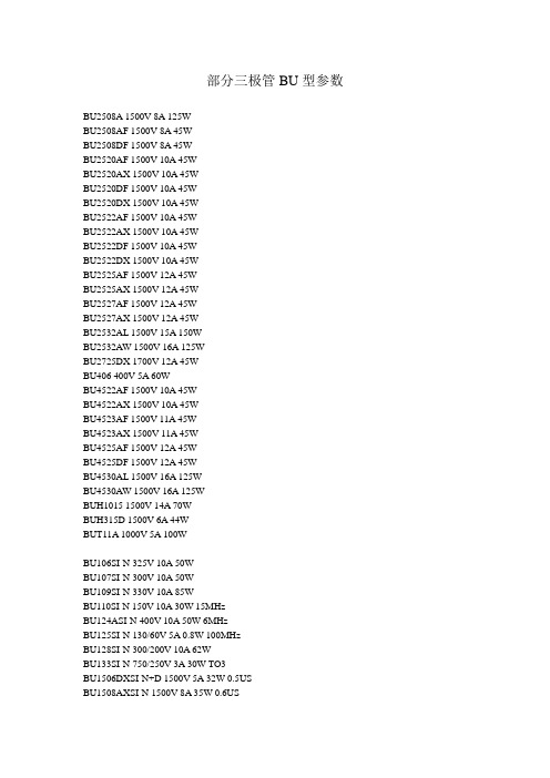
部分三极管BU型参数BU2508A 1500V 8A 125WBU2508AF 1500V 8A 45WBU2508DF 1500V 8A 45WBU2520AF 1500V 10A 45WBU2520AX 1500V 10A 45WBU2520DF 1500V 10A 45WBU2520DX 1500V 10A 45WBU2522AF 1500V 10A 45WBU2522AX 1500V 10A 45WBU2522DF 1500V 10A 45WBU2522DX 1500V 10A 45WBU2525AF 1500V 12A 45WBU2525AX 1500V 12A 45WBU2527AF 1500V 12A 45WBU2527AX 1500V 12A 45WBU2532AL 1500V 15A 150WBU2532AW 1500V 16A 125WBU2725DX 1700V 12A 45WBU406 400V 5A 60WBU4522AF 1500V 10A 45WBU4522AX 1500V 10A 45WBU4523AF 1500V 11A 45WBU4523AX 1500V 11A 45WBU4525AF 1500V 12A 45WBU4525DF 1500V 12A 45WBU4530AL 1500V 16A 125WBU4530AW 1500V 16A 125WBUH1015 1500V 14A 70WBUH315D 1500V 6A 44WBUT11A 1000V 5A 100WBU106SI-N 325V 10A 50WBU107SI-N 300V 10A 50WBU109SI-N 330V 10A 85WBU110SI-N 150V 10A 30W 15MHzBU124ASI-N 400V 10A 50W 6MHzBU125SI-N 130/60V 5A 0.8W 100MHzBU128SI-N 300/200V 10A 62WBU133SI-N 750/250V 3A 30W TO3BU1506DXSI-N+D 1500V 5A 32W 0.5USBU1508AXSI-N 1500V 8A 35W 0.6USBU1508DXSI-N+D 1500V 8A 35W 0.6US BU180ASI-N+D 400V 10ABU180EN-DARL 1500V 5A 12WBU189N-DARL 330V 8A 60WBU208ASI-N 1500V 8A 150W THIN B BU208BSI-N 700V 5A 80W 7MHzBU208DSI-N+D 1500V 8A 150WBU209SI-N 1700V 4A 12.5W TO3BU226SI-N 2000V 1.5A 10W TO3BU2506DFSI-N+D 1500V 5A 45W 0.4us BU2506DXSI-N+D 1500V 5A 45W 0.4US BU2508ASI-N 1500V 8A 125W 0.4usBU2508AFSI-N 1500V 8A 45W 0.4usBU2508AXSI-N 1500V 8A 45W 0.4US BU2508DSI-N+D 1500V 8A 125W 0.4us BU2508DFSI-N+D 1500V 8A 45W 0.4us BU2508DXSI-N+D 1500V 8A 45W 0.4us BU2520AFSI-N 1500V 10A 45W 0.2us BU2520AXSI-N 1500V 10A 45W 0.2us BU2520DFSI-N+D 1500V 10A 45W 0.35 BU2520DXSI-N+D 1500V 10A 45W 0.35 BU2525ASI-N 1500V 12A 0.2usBU2525AFSI-N 1500V 12A 45W 0.2us BU2525AXSI-N 1500V 12A 45W 0.2US BU2525DSI-N+D 1500V 12A 0.2usBU2527AFSI-N 1500V 12A 45W 0.2us BU2527AXSI-N 1500V 12A 45W 0.2US BU2722AFSI-N 1700V 10A 45WBU312SI-N 280/150V 6A 25WBU325SI-N 200/200V 3A 25WBU326ASI-N 900V 6A 75WBU326S-RFTSI-N 800/400V 6A 60W TO3 BU406SI-N 400V 7A 65W 0.75usBU406DSI-N+D 400V 7A 65W 0.75us BU407SI-N 330V 7A 65W 0.75usBU407DSI-N+D 330V 7A 65W 0.75us BU409DSI-N+D 250V 7A 60WBU412SI-N+D 280V 8ABU413SI-N 330V 10A 60W TO3BU414BSI-N+D 900V 8A 60WBU415ASI-N 800V 12A 120W TO3BU415BSI-N+D 800V 12A 120WBU426ASI-N 900V 6A 114WBU426ESI-N 800V 6A 70W TO220BU433SI-N 375V 6A 70WBU500SI-N 1500V 6A 75WBU500DSI-N+D 1500/700V 6A 75WBU505SI-N 1500V 2.5A 75W 0.9usBU505DSI-N+D 1500V 2.5A 75WBU505DFSI-N+D 1500V 2.5A 20WBU506SI-N 700V 5A 100W POWERBU506DSI-N+D 700V 5A 100W POWER BU506DFSI-N+D 1500V 5A 20W POWER BU508ASI-N 1500V 8A 125W 0.7usBU508ASI-N 1500V 8A 125W 0.7usBU508ASI-N 1500V 8A 125W 0.7usBU508AFSI-N 1500V 8A 34W 0.7usBU508AFSI-N 1500V 8A 34W 0.7usBU508AFSI-N 1500V 8A 34W 0.7usBU508DSI-N+D 1500V 8A 125W 0.7us BU508DSI-N+D 1500V 8A 125W 0.7us BU508DFSI-N+D 1500V 8A 34W 0.7us BU508DFSI-N+D 1500V 8A 34W 0.7us BU508DRSI-N+D 1500V 8A 125WBU522N-DARL 400/375V 7A 75WBU526SI-N 800V 8A 86WBU536SI-N 1100V 8A 62WBU546SI-N 1350V 6A 100W TO3BU603SI-N 1350V 5A 100W 0.7usBU606DSI-N+D 400V 7A 90WBU608SI-N 400V 6A 90W TO3BU608DSI-N+D 400V 7A 90WBU626ASI-N 1000V 10A 100WBU705SI-N 1500V 2.5A 75W 0.7usBU706DFSI-N+D 1500V 5A 32W 0.7us BU706FSI-N 1500V 5A 32W 0.7usBU801SI-N+D 600V 3A 40WBU806N-DARL+D 400V 8A 60W 0.35 BU806FISI-N+D 400V 8ABU808DFN-DARL+D 1500/700V 5A 50W BU810N-DARL+D 600V 7A 75WBU824N-DARL+D 650V 0.5ABU826N-DARL+D 800V 6A 125W 0.2 BU826AN-DARL+D 900V 6A 125W 0.2 BU920PN-DARL 350V 10A 120WBU921PSI-N 400/450V 10A 120WBU931SI-N 500V 15A 175WBU932N-DARL 500V 15A 175WBU932PN-DARL 500V 15A 125WBU941PN-DARL 500V 15A 150WBU941ZPN-DARL 350V 15A 150WBUF405ASI-N 1000/450V 7.5A 80WBUF405AFSI-N 1000V 7.5A ISOLATEDBUF410SI-N 850V 15A 125WBUH1015SI-N 1500V 14A 160W 0.11usBUH1015HISI-N 1500V 14A 70W 0.11usBUH1215SI-N 1500V 19A 200W 0.11usBUH315SI-N 1500V 5A 50WBUH315DSI-N+D 1500/700V 5A 50WBUH515SI-N 1500V 8A 60W 3.9usBUH515DSI-N+D 1500/700V 8A 60WBUH517SI-N 1700V 8A 60W 3.9usBUH517DSI-N+D 1700/700V 8A 60WBUH715SI-N 1500V 10A 60WBUK436/800BN-FET 800V 4A 125W <4EBUK437/400BN-FET 400V 14A 180WBUK437/600BN-FET 600V 9A 180W <1E2BUK438/800BN-FET 800V 7.6A 220W 2EBUK443/60BN-FET 60V 13A 25WBUK444/800BN-FET 800V 1.2A 30W 8EBUK445/600BN-FET 600V 2.2A 30W 2R5BUK446/800BN-FET 800V 2A 30WBUK454/800AN-FET 800V 2A 75WBUK455/600BN-FET 600V 4A 100W 2R5BUK456/200BN-FET 200V 19A 150WBUK456/60AN-FET 60V 52A 150W 0.028E《电子技术在线》—电子爱好者的家园TOP发短消息加为好友huangyan 当前离线UID2 帖子2377 精华35 积分1393 阅读权限200 在线时间44 小时注册时间2008-7-17 最后登录2009-5-31管理员40#huangyan发表于2008-9-30 17:38 | 只看该作者BUK456/800AN-FET 800V 4A 125W 3EBUK555/60BN-FET 60V 35A 125W 0.055EBUL310SI-N 1000V 5A 75W 0.4usBUL310PISI-N 1000V 5A 35W 0.4usBUL45SI-N 400V 5A 75W 12MHzBUL54ASI-N 1000V 4A 65W 20MHzBUL810SI-N 1000V 15A 125WBUR51SI-N 300/200V 60A 350WBUR52SI-N 350/250V 60A 350WBUS14ASI-N 1000/450V 30A 250WBUS23SI-N 300V 15A 175WBUS48ASI-N 1000V 15A 175WBUS48APSI-N 1000V 15A 125WBUS98ASI-N 450V 30A 250WBUT11ASI-N 1000V 5A 100W 0.8usBUT11ASI-N 1000V 5A 100W 0.8usBUT11AFSI-N 1500V 5A 20W 0.8usBUT12ASI-N 1000V 8A 125W 0.8usBUT12AFSI-N 1000V 8A 23W 0.8usBUT13N-DARL+D 400V 28A 175WBUT18ASI-N 1000/450V 6A 110W 0.BUT18AFSI-N 1000V 6A 33W 0.8usBUT30VSI-N 200/125V 100A 250WBUT34N-DARL+D 850V 50A 250WBUT56ASI-N 1000V 8A 100WBUT57N-DARL+D 400V 15A 110W B>BUT70SI-N 200V 40A 200WBUT72SI-N 400V 40A 200WBUT76ASI-N 1000V 10A 100W 0.8usBUT90SI-N 200V 50A 250WBUT92SI-N 350/250V 50A 250WBUT93SI-N 600V 4A 55W 9MHzBUV18SI-N 120V 47A 250W 1.5usBUV20SI-N 160V 50A 250W 1.5usBUV21SI-N 250/200V 40A 250WBUV23SI-N 325V 40A 250WBUV24SI-N 400V 30A 250WBUV25SI-N 500V 20A 250WBUV26SI-N 180V 14A 85W 1.8usBUV26ASI-N 200V 20A 85WBUV27SI-N 240V 12A 65W 40nsBUV28ASI-N 450V 10A 65W 40NS BUV46ASI-N 1000/450V 6A 85W BUV48ASI-N 1000V 15A 150W 0.8us BUV48AFSI-N 1000V 15A 65WBUV48CSI-N 1200/700V 15A 150W BUV48CFSI-N 1200V 15A 65WBUV50SI-N 250V 25A 150WBUV56ASI-N 1000V 10A 70WBUV61SI-N 300V 50A 250WBUV70SI-N 1300/550V 10A 140W BUV90N-DARL+D 650V 10A 125W BUV93SI-N 600/350V 2A 15W 12MHz BUV98ASI-N 1000V 30A 150W 5MHz BUW11ASI-N 1000V 5A 100W 0.8us BUW11AFSI-N 1000V 5A 32W 0.8us BUW12SI-N 850V 8A 125W 0.8us BUW12ASI-N 1000V 8A 125W 0.8us BUW12FSI-N 850V 8A 34W 0.8us BUW13SI-N 850V 15A 175W 0.8us BUW13ASI-N 1000V 15A 175W 0.8us BUW23SI-P 450V 10A 125W <300NS BUW26SI-N 800V 10A 125W 20MHz BUW42SI-P 400V 15A 150WBUW48SI-N 120V 30A 150W 1.5us BUW49SI-N 160V 30A 150WBUW50SI-N 250V 25A 150W TO-218 BUW72SI-N 450V 10A 100WBUW81AN-DARL 800V 10A 80WBUW84SI-N 800V 2A 50W 0.4us BUW85SI-N 1000V 2A 50W 0.4us BUX10SI-N 160V 25A 150W 1.5us BUX12SI-N 300V 20A 150WBUX13SI-N 400V 15A 150W >8MHz BUX20SI-N 160V 50A 350W 1.5us BUX22SI-N 300V 40A 250W POWSWI BUX23SI-N 400/325V 30A 350W BUX24SI-N 450/400V 20A 350W >8 BUX32BSI-N 1000V 8A 150WBUX37N-DARL 400V 15A 35WBUX39SI-N 120/90V 30A 120W 8MHzBUX41SI-N 250V 15A 120WBUX41NSI-N 220/160V 18A 120WBUX42SI-N 300V 12A 120WBUX48ASI-N 1000V 15A 175W 0.8usBUX51SI-N 300/200V 3.5A 10W >8BUX54SI-N 450V 2A 10W >8MHzBUX55SI-N 450V 2A 10W 8MHzBUX66SI-P 200/150V 2A 35W >20MHzBUX77SI-N 100V 5A 40W >2.5MHzBUX80SI-N 800V 10A 100WBUX81SI-N 1000V 10A 100WBUX82SI-N 800V 6A 60WBUX84SI-N 800V 2A 40W 0.4usBUX85SI-N 1000V 2A 40W 0.4usBUX85FSI-N 1000V 2A 18W 0.4usBUX86PSI-N 800V 0.5A 20W 0.4usBUX87SI-N 1000V 0.5A 20W 0.4usBUX87PSI-N 1000V 0.5A 20W 0.4usBUX88SI-N 1500V 12A 160W 7MHzBUX98ASI-N 450V 30A 250WBUX98CSI-N 1200V 30A 250W 5MHzBUY18SSI-N 80/40V 10A 20WBUY47SI-N 150/120V 7A 10W 90MHzBUY49PSI-N 250V 3A 10WBUY49SSI-N 250V 3A 10W 50MHzBUY69ASI-N 1000V 10A 100W 1usBUY70ASI-N 1000/400V 10A 75WBUY71SI-N 2200V 2A 40W HORDEFLBUY72SI-N 280/200V 10A 60WBUY89SI-N 1500V 6A 80W《电子技术在线》—电子爱好者的家园-TOP发短消息加为好友huangyan 当前离线UID2 帖子2377 精华35 积分1393 阅读权限200 在线时间44 小时注册时间2008-7-17最后登录2009-5-31管理员42#huangyan发表于2008-9-30 17:39 | 只看该作者BUZ10N-FET 50V 20A 80W 0.08RBUZ100N-FET 50V 60A 250W 0.18EBUZ11N-FET 50V 36ABUZ11AN-FET 50V 27A 90W 0.055RBUZ14N-FET 50V 39A 125WBUZ15N-FET 50V 45A 125WBUZ171P-FET 50V 8A 40W 0.3RBUZ21N-FET 100V 21ABUZ215N-FET 500V 5A 75W <1E5BUZ22N-FET 100V 34A 125W 0.055BUZ30AN-FET 200V 7A 75WBUZ310N-FET 1000V 2.5A 75W <5EBUZ325N-FET 400V 12.5A 125WBUZ326N-FET 400V 10.5A 125WBUZ330N-FET 500V 9.5A 125W 0E6BUZ332N-FET 600V 8.5A 150W 0.8RBUZ332AN-FET 600V 8A 150W 0.9EBUZ338N-FET 500V 13.5A 180WBUZ341N-FET 200V 33A 170W 0.07EBUZ345N-FET 100V 41A 150WBUZ349N-FET 100V 32A 125WBUZ380N-FET 1000V 5.5A 125W 140BUZ384N-FET 500V 10.5A 125WBUZ50AN-FET 1000V 2.5A 75W 5EBUZ71N-FET 50V 18A 80W 0.1RBUZ71AFN-FET 50V 11A 35W 0.12RBUZ72AN-FET 100V 11ABUZ72AFN-FET 100V 10A 40W ISOLATBUZ73N-FET 200V 7A 40W 0.4RBUZ73AN-FET 200V 5.8A 40W 0.6RBUZ90N-FET 600V 4.5A 70W <1E6BUZ900N-FET 160V 8A 125WBUZ901N-FET 200V 8A 125WBUZ905P-FET 160V 8A 125WBUZ906P-FET 200V 8A 125WBUZ90AN-FET 600V 4A 75W 2RBUZ90AFN-FET 600V 4.3A 75WBUZ91AN-FET 600V 8A 150W 0.9RBUZ93N-FET 600V 3.6A 80W <2E5《电子技术在线》—电子爱好者的家园TOP发短消息加为好友huangyan 当前离线UID2 帖子2377 精华35 积分1393 阅读权限200 在线时间44 小时注册时间2008-7-17 最后登录2009-5-31管理员43#huangyan发表于2008-9-30 17:39 | 只看该作者BU1506DXSi.N+D150058322503,8...7,5<1BU1508AXSi.N1500815354003,5...7,5<5BU1508DXSi.N+D1500815354005,5…7.5<5BU1706ASi.N175058100250>8<1BU1706AXSi.N175********>8<1BU2506DFSi.N+D150058452503,8...7,5<1BU2506DXSi.N+D150058452503,8...7,5<1BU2507AXSi.N1500815452505...9<5BU2508ASi.N15008151254004...7,5<5BU2508AFSi.N1500815454004…7.5<5BU2508AXSi.N1500815454004…7.5<5BU2508DSi.N+D15007151254004…7.5<5BU2508DFSi.N+D1500715454004…7.5<5BU2508DXSi.N+D1500715454004…7.5<5BU2515DXSi.N+D150092045200(56kHz)5...10<5BU2520ASi.N150010251252005...10<5BU2520AFSi.N15001025452005...10<5BU2520AXSi.N15001025452005...10<5BU2520DSi.N+D150010251253505...10<5BU2520DFSi.N+D15001025453505...10<5BU2520DXSi.N+D15001025453505...10<5BU2522ASi.N150010251251205...8<5BU2522AFSi.N15001025451205...8<5BU2522AXSi.N15001025451205...8<5BU2522DXSi.N+D15001025451205...10<5BU2523AFSi.N1500112945150(64kHz)5…10<5BU2525ASi.N150012301252005...10<5BU2525AFSi.N15001230452005...10<5BU2525AXSi.N15001230452005…10<5BU2525DFSi.N+D15001230452005...9<5BU2527ASi.N15001230125100(64kHz)5...9<5BU2527AFSi.N15001230451005...9<5BU2527AXSi.N15001230451005...9<5BU2527DXSi.N+D15001230451005...10<5BU2530ALSi.N150********<35010...30(1A)<5BU2530AWSi.N150016401251405,5…10<5BU2532ALSi.N1500164012560(82kHz)6…12,5<5 BU2532AWSi.N1500164012560(82kHz)6…12,5<5 BU2708AFSi.N1700815454003...7,3<1BU2708DFSi.N+D1700815454003...7,3<1BU2720AFSi.N17001025457004...7,5<1BU2722AFSi.N17001025451904...10<1BU2725DXSi.N+D1700123045600(16khz)3,8...7,5<1 BU2727ASi.N1700123012564kHz5,5...11<1BU2730ALSi.N1700164012532kHz5...9<5BU4506AFSi.N150058453004,2...7,3<3BU4506DXSi.N+D150058453004,2...7,3<3BU4506DZSi.N+D150058323004,2...7,3<3BU4507DXSi.N+D1500815453004,2...7,3<3BU4508DFSi.N+D1500815453004,2...7,3<3BU4515AFSi.N150092045230(64kHz)4,2...7,3<3 BU4515DFSi.N+D150********kHz4,2...7,3<3BU4522DFSi.N+D150010254564kHz4,2...5,8<3BU4523DFSi.N+D150011294570kHz4,2...5,8<3BU4525DFSi.N+D150012304570kHz4,2...5,8<3BU4525DLSi.N+D1500143012570kHz4,2...5,8<3 BU4530ALSi.N15001640125120(90kHz)4,8...8,5<3 BU4530AWSi.N15001640125120(90kHz)4,8…8,5<3 BU4530AXSi.N1500164045120(90kHz)4,2…6.5<3 BU4540ALSi.N15002540125110kHz4,2…6,5<3BU4540AWSi.N15002540125110kHz4,2…6,5<3BU4550ALSi.N15002540125130kHz4,2…6,5<3BU508AFSi.N1500815357006...13<3BU508AFISi.N1500815505506...13<3BU508D(Sanyo)Si.N+D150051650400>2,5<1,3BU808DFISi.N+Darl14008105280060...230<1,6 BUH1015Si.N150014181601107…14<1,5BUH1015HISi.N15001418701107…14<1,5BUH1215Si.N150016222001107...14<1,5BUH313Si.N130********>3.5<1,5BUH313DSi.N+D130********>3.5<1,5BUH315Si.N1500612442703.,5…12<1,5BUH315DSi.N+D1500612444002,5…9<1,5BUH417Si.N170071255330>4<1,5BUH515Si.N1500812502006...12<1,5BUH515DSi.N+D1500815504505...10<1,5BUH517Si.N1700815602004…6<1,5BUH715Si.N15001020573205...16<1,5《电子技术在线》—电子爱好者的家园TOP发短消息加为好友huangyan 当前离线UID2 帖子2377 精华35 积分1393 阅读权限200 在线时间44 小时注册时间2008-7-17 最后登录2009-5-31管理员44#huangyan发表于2008-9-30 17:39 | 只看该作者BUH517D SI-N+D 1700/700v, 8A, 60wBU2506AF1500V3.5A50W--BU2507AF1500V6A45W--BU2508AF1500V8A45W--BU2520AF1500V10A45W--BU2522AF1500V10A80W--BU2523AF1500V10A80W--BU2525AF1500V12A80W--BUW11AF1000V5A100W--BUW13AF1000V15A175W--BUW48AF1000V60A150W--BUT12A1000V10A100W--BUS13A1000V15A125W--BUX48A1000V7A175W--BUX48C1200V15A175W--BUX851000V3A40W--BUX98A1000V30A250W--BU2506DF1500V3.5A50W*BU2507DF1500V6A125W*BU2508DF1500V8A125W*BU2520DF1500V10A125W*BU2522DF1500V10A80W*BU2523DF1500V10A80W*BU2525DF1500V12A125W*BUW12AF1000V8A125W--BUW14AF1000V20A175W--BUT11A1000V5A100W--BUS12A1000V8A125W--BUS14A1000V30A250W--BUX48B1100V10A175W--BUX84800V2A40W--BUX861200V4A40W--BUX98B1200V30A250W--《电子技术在线》—电子爱好者的家园TOP发短消息加为好友huangyan 当前离线UID2 帖子2377 精华35 积分1393 阅读权限200 在线时间44 小时注册时间2008-7-17 最后登录2009-5-31管理员45#huangyan发表于2008-9-30 17:39 | 只看该作者BU208ANPN12彩行1500V5A12.5WBU208DNPN12彩行1500V5A12.5W (带阻尼)BU323NPN28达林顿功放450V10A125WBU406NPN28行管400V7A60WBU508ANPN28行管1500V7.5A75WBU508ANPN28行管1500V7.5A75W 原BU508DNPN28行管1500V7.5A75W (带阻尼)BU806NPN28功放400V8A60W DAR-LBU932RNPN12功放500V15A150W DAR-LBU941NPN12BU1508DXNPN28开关功放BU2506DXNPN30开关功放1500V7A50W /600NSBU2508AFNPN30开关功放700V8A125W /600NSBU2508AXNPN30开关功放700V8A125W /600NSBU2508DFNPN30开关功放700V8A125W/600NS(带阻尼) BU2508DXNPN30开关功放1500V8A50W/600NS(带阻尼) BU2520AFNPN30开关功放800V10A150W 1/500NSBU2520AXNPN30开关功放1500V10A150W 1/500NSBU2520DFNPN30开关功放800V10A150W1/500NS(带阻) BU2520DXNPN30开关功放1500V10A50W/600NS (带阻) BU2522AFNPN30开关功放1500V11A150W /350NSBU2522AXNPN30开关功放1500V11A150W /350NSBU2525AFNPN30开关功放1500V12A150W /350NSBU2525AXNPN30开关功放1500V12A150W /350NSBU2527AFNPN30开关功放1500V15A150WBU2532AWNPN30开关功放1500V15A150W(大屏)BUH515NPNBCE行管1500V10A80WBUH515DNPNBCE行管1500V10A80W(带阻尼)BUS13ANPN12开关功放1000V15A175WBUS14ANPN12开关功放1000V30A250WBUT11ANPN28开关功放1000V5A100WBUT12ANPN28开关功放450V10A125WBUV26NPN28音频功放开关90V14A65W /250nsBUV28ANPN28音频功放开关225V10A65W /250nsBUV48ANPN30音频功放开关450V15A150WBUW13ANPN30功放开关1000V15A150WBUX48NPN12功放开关850V15A125WBUX84NPN30功放开关800V2A40WBUX98ANPN12功放开关400V30A210W5MHZ。
Single output step down (Buck) Converter Vin max < 7VSY8018A 2.5 5.5 0.45 / 0.6 ±2% 1.5 400/200 √Ultra Low Quiescent Current DFN2x2-8 SY8030L 2.5 5.5 0.6 2.25 0.6 ±1.5% 50 300/200 DFN2x2-6 SY8078B 1.85 5.5 0.6 3 0.4 ±2% 40 350/250 DFN1.45x1-6 SY8010 2.5 5.5 1 1.5 0.6 ±1.5% 50 200/150 DFN2x2-6 SY8011A 2.5 5.5 1 1.5 0.6 ±2% 40 230/150 DFN1.5x1.5-6 SY8061A 2.5 5.5 1 1.5 0.6 ±2% 60 260/170 Auto Discharge DFN2x2-6 SY8065L 2.5 5.5 1 1.5 0.6 ±2% 90 250/200 √SOT 23-6 SY8071 2.5 5.5 1 2 0.6 ±2% 40 260/170 SOT 23-5 SY8075 2.5 6.5 1 1.5 0.6 ±2% 40 260/170 DFN2x2-6 SY8077 2.5 6.5 1 1.5 0.6 ±2% 40 260/170 SOT 23-5 SY8080 2.5 5.5 1 3 0.6 ±2% 40 270/160 SOT 23-5SY8081 2.5 5.51 2.5 0.6 ±2%40230/150 Output auto discharge DFN1.5×1.5-6SY8011B 2.5 5.5 1.5 1.5 0.6 ±2%60210/130 DFN1.5x1.5-6SY8030 2.5 5.5 1.5 2.25 0.6 ±1.5%50200/150 Ext Mode DFN2x2-6 SY8002B 2.7 5.5 1.5 1 0.6 ±2% / 110/80 √Latch off protection SOT 23-6SY8002E 2.7 5.5 2 1 0.6 ±2% / 110/80 √Force PWM SOT 23-6SY8003L 2.7 5.5 2 1 0.6 ±2% 55 120/90 √DFN2x2-8Single output step down (Buck) Converter Vin max < 7V±2%SY8089 SOT 23-52.7 5.5 2 1 0.6 55 110/80 Latch off protectionSY8003C1 2.7 5.5 3 3 0.6 ±2% 55 110/80 √DFN2x2-8SY8823 2.5 5.5 3.5 2 0.6 ±1.5% 18 55/35 √QFN2x1.5-8SY8047 2.5 5.54 1.25 0.6 ±1.5%1875/55√QFN3x3-16SY8856 2.7 5.54 3 0.6 ±1.5%6035/15 √√DFN2x2-8√±1.5%SY8003F 2.7 5.5 3 1 0.6 / 110/80 DFN2x2-8 SY8079P 2.7 6.5 0.6 ±2% 55 125/95 Non latch off OVP SOT 23-6SY8032 2.7 5.5 2.5 0.6 ±2% 80 100/80 SOT 23-6SY8032E 2.7 5.5 2.5 0.6 ±2% 100/80 Force CCM SOT 23-6SY8003 2.7 5.5 0.6 ±2% 55 110/80 Latch SCP/OVP DFN2x2-8SY8003A 2.7 5.5 0.6 ±2% 55 110/80 Non-latch off protection DFN2x2-8SY8003C 2.7 5.5 0.6 ±2% 55 100/80 DFN2x2-8 SY8003E 2.7 5.5 0.6 ±2% 110/80 Force CCM DFN2x2-8 SY8043A 2.7 5.5 1.25 0.6 ±2% 18 75/55 DFN3x3-16 SY8047L 2.5 5.5 1.25 0.6 ±2% 18 75/55 QFN3x3-16 SY8859 2.7 5.5 0.6 ±1% 40 100/50 OVP/OCP/SCP/UVLO/OTP QFN1.5x1.5-7Single output step down (Buck) Converter Vin max < 7VPart Number Vin (min)(V)Vin (max)(V)Iout (max) (A) Fsw (MHz)Vout (min)( V)VoltageAcurracySY8824B 2.6 5.5 4 1.8 / ±1% SY8824C 2.6 5.5 4 1.8 / ±1% SY8035 2.7 5.5 5 1 0.6 ±1.5% SY8805A 3 5.5 5 1 0.6 ±1.5% SY8825 2.5 5.5 5 2 0.6 ±1.5% SY8876 2.7 6.5 6 1.2 0.6 ±1.5% SY8827K 2.5 5.5 6 2.4 ±1.5% SY8868 2.7 5.56 10.6 ±1% SY8099 2.7 5.5 6 1 0.6 ±1% SY8812 2.75 5.5 12 1 ±1%80 70/40Programmable Output Voltage: 0.7625Vto 1.55V in 12.5mV/step; Default 1.15Voutput voltage8015010018606550408070/4050/4035/1555/3538/1528/1735/1530/1212/6PackageTSOT 23-8Programmable Output Voltage: 0.7625Vto 1.55V in 12.5mV steps; Default 1.05Voutput voltageTSOT 23-8EXT SS DFN3x3-10DFN2x2-8QFN2x1.5-8OCP/UVLO/OTP DFN2x2-8I2C Programmable Vout: 0.7125V~ 1.5V CSP1.56x1.96-20in 12.5mV steps, Addr: 1000001xCOT mode,max dutyHigh efficiencyP rogrammable Output Voltage: 0.6V to1.5V in 10mV stepsQFN2x2-10TSOT 23-6QFN3x3-12Dual output step down (Buck) Converter Vin max < 7VPart Number Vin(min)(V)Vin(max)(V)Iout(max)(A)Fsw (MHz) Vout (min)(V)VoltageAcurracyQuiescentCurrent(uA)MO SFET Ron H/L (m? ) Power GoodOutputFeature/ Special Function PackageSY8020 2.5 5.5 1A x2 1.5 0.6 ±2% 50 200/150 Individual EN DFN3x3-12 SY8831 2.5 5.5 1A x2 1.5 0.6 ±2% 45/55 260/180 Individual EN TSOT 23-8 SY8832 2.5 5.5 2A x2 2 0.6 ±2% 35/45 125/100 Individual EN TSOT 23-8 SY8024 3 5.5 3A x2 1 0.6 ±2% 80 105/85 Individual EN DFN3x3-12 SY8821 2.5 5.5 1A/1.5A 2 0.6 ±2% 45 125/100 Individual EN DFN2x1.5-8Single output step down (Buck) Converter, Vin max > 7VuiescentOriginal Part Number Vin(min)(V)Vin(max)(V)Iout(max)(A)Fsw (MHz) Vout( imn)(V)Fixed O utputVoltage(V)VoltageAcurracyCurrent (uA)MOSFET(RonH/L) (m ? )Power oGodOutputFeature/ Special Function PackageSY8290 5 40 0.3 2 0.6 ±2.0% 160 2000/- SOT 23-6 SY8200 6 24 0.6 0.5 0.6 ±2% 400 420/200 SOT 23-6 SY8401 4.5 50 0.8 1.2 0.6 ±1.0% 150 700/- SOT 23-6SY8201 4.527 1 0.5 0.6 ±2%400350/150 SOT 23-6SY8201C 4.527 1 1.15 0.6 ±2%400350/150 Force CCM SOT 23-6SY85017 100 1 0.2~1MHz 1.2 ±2.0%400500/240 Programmable Switching Frequency SO8ESY8291 5 40 1.2 0.8 0.6 ±2.0% 160 180/- SOT 23-6 SY8502 7 100 1.8 0.2~1MHz 1.2 ±2.0% 400 500/240 Programmable Switching Frequency SO8ESingle output step down (Buck) Converter, Vin max > 7VVin(min) Vin(max) Iout(max) Fsw Vout(min) Voltage Quiescent MO SFET(Ron Power GoodPart Number(V) (V) Iout((m A)ax)(MHz) (V) Acurracy Current (uA) H/L) (m ? ) O utputFeature/ Special Function PackageSY8121 4.5 18 2 1 0.6 ±2% 400 170/160 SOT 23-6/ DFN2x2-6 SY8121B 4.35 18 2 1.2 0.6 ±2% 170/160 1.2MHz, FCCM SOT 23-6SY8120B1 4.5 18 2 0.5 0.6 ±2% 400 130/120 SOT 23-6SY8121C 4.5 18 2 1.2 0.6 ±2% 400 130/120 SOT 23-6SY8222 4.5 23 2 0.5 0.6 ±1.5% 400 150/110 √EXT SS, Hic-cup SCP DFN3x3-10SY8292 5 40 2 0.8 0.6 ±2.0% 160 180/- SOT 23-6SY8113B 4.5 18 3 0.5 0.6 ±1.5% 100 80/40 Hic-cup SCP TSOT 23-6SY8113C 4.518 3 1 0.6 ±1.5%10080/40 Hic-cup SCP TSOT 23-6SY8113D 4.5 18 3 0.5 0.6 ±1.5% 100 80/40 √Hic-cup SCP, EXT SS TSOT 23-8SY8113G 4.518 3 0.5 0.6 ±1.5%10080/40 Hic-cup SCP, FCCM TSOT 23-6SY8203A 4.523 3 1 0.6 ±1.5%400120/85 √EXT SS DFN3x3-10SY8223 4.523 3 0.5 0.6 ±1.5%400120/85 √EXT SS, Hic-cup SCP DFN3x3-10SY8253 4.5 23 3 0.5 0.6 ±1.5% 100 105/50 √EXT SS, Hic-cup SCP TSOT 23-8SY8303 4.5 40 3 0.5~2.5MHz 0.6 ±1.5% 18 70/110 TSOT 23-8 SY8293 5 40 3 0.8 0.6 ±2.0% 160 180/-SO8EPart Number Vin(min)(V)Vin(max)(V)Iout(max)(A)Fsw (MHz) Vout(min)(V)VoltageAcurracyQuiescentCurrent (uA)MO SFET(Ron H/L)(m ? )Power Good OutputFeature/ Special Function PackageSY8502 7 85 1.2 0.2~0.5 1.2 ±2.0% / 500/240 Programmable Switching FrequencyRangeSO8ESY8120B1 4.5 18 2 0.5 0.6 ±2% 400 130/120 SOT 23-6SY8121 4.5 18 2 1 0.6 ±2% 400 170/160 SOT 23-6/ DFN2x2-6 SY8121C 4.5 18 2 1.2 0.6 ±2% 400 130/120 SOT 23-6SY8222 4.5 23 2 0.5 0.6 ±1.5% 400 150/110 √EXT SS, Hic-cup SCP DFN3x3-10SY8292 5 40 2 0.8 0.6 ±2.0% 160 180/- SOT 23-6SY8113B 4.5 18 3 0.5 0.6 ±1.5% 100 80/40 Hic-cup SCP TSOT 23-6SY8113C 4.5 18 3 1 0.6 ±1.5% 100 80/40 Hic-cup SCP TSOT 23-6SY8113D 4.5 18 3 0.5 0.6 ±1.5% 100 80/40 √Hic-cup SCP, EXT SS TSOT 23-8SY8113G 4.5 18 3 0.5 0.6 ±1.5% 100 80/40 Hic-cup SCP, FCCM TSOT 23-6SY8203A 4.5 23 3 1 0.6 ±1.5% 400 120/85 √EXT SS DFN3x3-10SY8223 4.5 23 3 0.5 0.6 ±1.5% 400 120/85 √EXT SS, Hic-cup SCP DFN3x3-10SY8253 4.523 3 0.5 0.6 ±1.5%100105/50 √EXT SS, Hic-cup SCP TSOT 23-8SY8303 4.5 40 3 0.5~2.5MHz 0.6 ±1.5% 18 70/110 TSOT 23-8SY82935 40 3 0.8 0.6 ±2.0%160180/- SO8ESY8113H 4.5 18 3 0.5 0.6 ±1.5% 160 80/40 Programmable soft-start time TSOT 23-8±1.5%SY8104A4.518 4 0.5 0.6±1.5%100 50/30Instant PWM architectureSY8105 4.5 18 5 0.5 0.6±1.5%100 50/30SY8205 4.5 30 5 0.5 0.6±1.5%200 70/40√EXT SSSY8105A 4.5 18 5 0.5 0.6±1.5%100 40/20Instant PWM architectureSY8366H 4 28 6 0.8 0.6±1.5%100 40/20√Hic-cup SCP, 12A Peak current capability,programmable output current limitSY8286A 4 23 60.6 0.6 ±1.0% 12038/19 √SY8366K428 6 0.50.6±1.5%10040/20√Hic-cup SCP,6A continuous/12A peakoutput current capabilitySY8368A42880.80.6±1%100 20/10√Hic-cup SCP, 16A Peak current capability,programmable output current limitSY8288A 4 23 8 0.5 0.6 ±1.0% 80 30/10SY8288 4 23 8 0.5 0.6 ±1.0%8030/10SY8288C5.52380.60.6±1.5%10822/11√OVP/OCPSY8210A 4 28 10 0.6 0.6±1.5%300 25/8√Mem o ry power, 10A VDDQ/1A VTT LDO, 16A Peak Current capability, Latch offUVP/OVP, Over temperature alertSY8204 4.5 30 40.50.620080/50EXT SSPackageTSOT 23-6SO8ETSOT 23-6TSOT 23-6DFN3x4-12TSOT 23-6QFN3x3-12QFN3x3-20QFN3x3-12QFN3x3-12QFN3x3-20 QFN3x3-20QFN3x3-20QFN4x3-19Part Number Vin(min)(V)Vin(max)(V)Iout(max)(A)Fsw (MHz) Vout(min)(V) Voltage AcurracyQuiescent Current (uA)MO SFET(Ron H/L) (m ? ) Power Good OutputFeature/ Special Function Package SY8182 4 18 12 0.2~1MHz 0.6 ±1.0%18/6 √QFN4x4-20SY8182L 4.5 18 12 0.2~1MHz0.6 ±1.0% 500 18/6 √ Hic-cup SCP/OVPQFN4x4-24 SY8186418160.50.6±1.5%1507.5/2.5√Hic-cup SCP, programmble outputQFN4x4-11current limitPart NumberVin(min)(V)Vin(max)(V)Ilim (A)Fsw (MHz)Vout(max)(V)Sync BoostFixed O utputVoltage (V) Acu F r B ra /c y AcurracyInput Q uiescent Current (uA)Q uiescent current from output (uA)MO SFET Ro n (L/S) (m ? )Feature/ Special Function PackageSY7060L 0.7 5 0.2 / 5.25 Y /0.5V ±3% 0.518450/800SOT-363SY7070 0.7 5 0.35 / / Y 3.3 /0.5 5.5 500/700Bypass function @ shutdown SOT 23-5SY7070A 0.7 5 0.35 / / Y 3 / 0.5 5.5 500/700SOT 23-5SY7071 0.7 5 0.35 / 5.25 Y /1.0V ±3%0.5 5 500/700 Pass-through function @ shutdown SOT-363SY7071A 0.7 5 0.35 / / Y 5 / 0.5 7 400/500Pass-through function @ shutdown SOT-363SY7060 0.7 5 0.4 / 5.25 Y /0.5V ±3% 0.5 18 450/800SOT-363SY7080 0.9 4 1.8 1.2 4 Y / 1.2V ±3%65 / 90/200 Output Disconnect @Shutdown SOT 23-6Single output step Up (Boost) Converter (Low V oltage)Part NumberVin(min)(V)Vin(max)(V)Ilim (A)Fsw (MHz)Vout(max)(V)Sync BoostFixed O utput Voltage (V)Acu F rr B a /c y Acurracy InputQuiescent Current (uA) Quies cent current from output (uA) MOSFET Ron(L/S) (m ?) Feature/ Special Function PackageSY7063 1.8 5.25 3 0.5 5.5 Y / 1.2V ±1.5% 102736/40Output Disconnect @Shutdown QFN2x2-10SY7069 2.5 5.5 3 1 5.5 Y / 1.2V±1.5% 8 32 50/90TSOT 23-6SY7088 2.3 5 3 1 5.5 Y / 1.2V ±1.5% 2 30 70/85DFN2x3-8SY7088E 2.3 5 3 1 5.5 Y / 1.2V ±1.5% / / 70/85DFN2x3-8SY7065 1.8 5.25 5 0.5 5.5 Y / 1.2V ±1.5% 10 27 20/40 Auto output discharge function QFN2x2-10SY7065A 1.8 5.25 5 0.5 5.5 Y / 1.2V ±1.5% 10 27 20/40No output discharge function QFN2x2-10SY7076 2 5.5 6 0.5 5.5 Y / 1.2V ±1.5% 10 27 20/40QFN2x2-10SY7066 1.8 5.25 6 0.5 5.5 Y / 1.2V ±1.5% 10 27 20/40 Auto output discharge function QFN2x2-10SY7066B 1.8 5.25 6 0.5 5.5 Y / 1.2V ±1.5%10 27 20/40 Selectable Forced PWM mode QFN2x2-10Single output step Up (Boost) Converter (Low V oltage)SY9701A 2.6 5.5 1.2 1 5.5 0.6V ±1.5% 60 100/100 Output Disconnect @Shutdown DFN3x3-14Single output step Up (Boost) Converter (High Voltage)PackagePart NumberVin(min)(V)Vin(max)(V)Ilim (A)Fsw (MHz) Vout (max) (V) Sync BoostFB/ AcurracyInput Q uiescent Current (uA) MO SFET (RonMain/Rectified)(m? )Disconnect FET Ron ( m ?) Power Good OutputFeature/ Special FunctionSY7208C 3 25 0.6 1 25 N0.6V ±2%100 150/-Int SS/CompSOT 23-6SY7152A 3 8 2 1 16 N0.6V ±2%100 130/-Int SS/Comp SOT 23-6SY7208L 3 25 2 1 25 N0.6V ±2%100 150/-Int SS/Comp SOT 23-6SY7302 3 33 2 1 33 N0.6V ±2% 100 200/-Int SS/Comp SOT 23-6SY7388 3.5 30 2 0.85 30 N 1V ±2%150 200/-Accurate input current limit SOT 23-6SY7102 2 6 2.5 1 6 N0.6V ±2% 200 120/-Int SS/Comp SOT 23-6SY7801 2.5 5.5 2.5 1 / N 0.6V ±2%200 120/-Int SS, with 2A 80m? Load Switch DFN3x3-12SY7104A2 6 4 1 6 N0.6V ±2% 100 90/-Int SS/Comp DFN3x3-10SY7304 3334133N 0.6V ±2%100120/-QFN3x3-10SY7205 8.6 15.9 4.5 0.5 16 N1.25V±1.5% 120 75/-Adjustable soft-start time, OVP DFN3x3-10SY7982 3 9 6 1 13 Y 1V ±2% 600 80/4040√True shutdown QFN3x3-16SY7219 3 5.5 9 / 36 N 1.25V ±2%350 65/-EXT Comp DFN3x3-10 SY721531615/18Y1V ±1.5% 22016/1818√Int SS, OVP/SCP/ True shutdown ProgrammableSwitching Frequency: 0.2~1MHz QFN4x4-18SY7215A31615/18Y 1V ±1.5%2309/1212√Int SS, OVP/SCP/ True shutdown ProgrammableSwitching Frequency: 0.2~1MHzQFN4x4-181.23VInt SS; Adjustable current limit for optical module;SY7501B2.955.50.930.480N ±2%225 800/-Current limit indicator; Accurate high-side currentQFN3x3-16monitor; 320mW maximum output powerDC-DC PWM Controller (external Switch)Original Part Number Vin(min)(V)Vin(max)(V)Fsw (MHz)V(V R)EFFunction PackageSY7901 3 25 0.5 1 Current mode DC/DC controller targeted for Boost, Sepic, Flyback and Forward applications with DC Input Current Limit DFN3x3-10 SY7902A 3 25 0.3 1 Current mode DC/DC controller targeted for both Boost and Sepic applications with DC Output Current Limit SOP10 Power ModulePart Number Vin(min)(V)Vin(max)(V)Iout(max)(A)Fsw (MHz)Fixed O utputVoltage (V)Voltage Acurracy Q uiescent Current (uA) MOSFET (Ron H/L) (m? ) Integrated Inductor PackageSY98081 2.5 5.5 0.6 3 ±2% 40 230/150 √QFN2x1.5-8 SY98001 2.5 5.5 1.2 3 ±2% 40 230/150 √QFN2.5x2-8 SY98003 2.7 5.5 3 3 ±1.5% 60 35/15 √QFN3x3-10 SY98004 2.7 5.5 4 3 ±1.5% 60 35/15 √QFN3x3-10 SY98002 2.7 5.5 2 3 ±1.5% 60 20/40 √QFN3x3-10 SY98202 4.5 23 2 2 ±1.5% 100 50/105 √QFN3x3-10 SY98195 4.5 18 5 1.5 ±1.5% 15/50 √QFN5x5-20LDO RegulatorPart Number Vin(min)(V)Vin(max)(V)Vout(V)Iout(A)Dropout Voltage (mV) Function PackageSY6340 2.3 30 Output Voltage Adjustable 0.15 300 LDO Reg SOT23-5D FN2×2-6 SY6340B 3.6 30 3.3 0.05 100 LDO Reg SOT 23-5SY6345 4 40 Adjustable 0.3 300 LDO Reg SOT 23-5SY6301 1.6 5.5 Output Voltage Adjustable 1 0.32V at I OUT =1A, V OUT =1.5V0.18V at I OUT =1A, V OUT =2.8VLDO Reg DFN3×3-6SY6307B 0.8 5.5 Output Voltage Adjustable 0.5 90 LDO Reg DFN1.2x1.2-6 Protection SwitchPart Number Package Enabl eLogic O CP O VP No. ofChannelsVin(V) Vout(V) Iout(A) Rds(on) TUV/CBCertificateULCertificateSpecial FunctionSY6280A SOT 23-5 H Y N 1 2.4~5.5 2.4~5.5 0.4~2 63m? Programmable current limit, reverse blockingSY6281A SOT 23-5 L Y N 1 2.4~5.5 2.4~5.5 0.4~2 63m? Programmable current limit, reverse blockingSY6288A SOT 23-5 H Y N 1 2.5~5.5 2.5~5.5 0.6 80m? √√Output discharge at shutdown Reverse Blocking,OCB indicatorSY6288B SOT 23-5 L Y N 1 2.5~5.5 2.5~5.5 0.6 80m? ? ? Output discharge at shutdown Reverse Blocking,OCB indicatorSY6811 CSP0.9x0.9-4 H N N 1 1.05~1.95 1.05~1.95 1 45m?@VIN=1.2V35m?@VIN=1.8V Auto output cap discharge function, utra low inputvoltageSY6819A SO8 H Y N 1 4.5~18 4.5~18 1.2 110m?@VIN=12V Programmable blanking t ime for DFF control, Default Off when EN ONSY6819 SO8 H Y Y 1 4.5~18 4.5~18 1.2 110m?@VIN=12V Programmable blanking t ime for DFF control,Default On when EN ONSY6288C20 SOT 23-5 H Y N 1 2.5~5.5 2.5~5.5 2 65m? ? ? Output discharge at shutdown Reverse Blocking,OCB indicatorSY6288D20 SOT 23-5 L Y N1 2.5~5.5 2.5~5.5265m? √√Output discharge at shutdown Reverse Blocking,OCB indicatorPart Number Package EnableLogicOCP OVPNo. ofChannelsVin(V) Vout(V) Iout(A) Rds(on)TUV/CBCertificateULCertificateSpecial FunctionSY6882A DFN2x2-8 H N Y 1 3~23 3~23 2 100m?Internal Fixed Over-Voltage Protection Threshold @7.1V, Thermal Shutdown Protection&Auto RecoverySY6882B DFN2x2-8 H N Y 1 3~23 3~23 2 100m? Programmable OVP Threshold Thermal Shutdown Protection& Auto RecoverySY6883 SOT 23-6 L N Y 1 3~23 3~23 2 100m? Programmable OVP Threshold Thermal Shutdown Protection& Auto RecoverSY6822 QFN2x2-10 L Y N 1 3~6.6 3~6 2 60m? Bidirectional Current Limit SwitchSY6288C7 SOT 23-5 H Y N 1 2.5~5.5 2.5~5.5 2.5 70m? √Output discharge at shutdown Reverse Blocking,OCB indicatorSY6288D7 SOT 23-5 L Y N 1 2.5~5.5 2.5~5.5 2.5 70m? √Output discharge at shutdown Reverse Blocking,OCB indicatorSY6288C5 MSOP8 H Y N 1 2.5~5.5 2.5~5.5 2.5 70m? √√Output discharge at shutdown Reverse Blocking,OCB indicatorSY6288D5 MSOP8 L Y N 1 2.5~5.5 2.5~5.5 2.5 70m? √√Output discharge at shutdown Reverse Blocking,OCB indicatorSY6288E1 SOT 23-5 H Y N 1 2.5~5.5 2.5~5.5 3 45m? √√Output discharge at shutdown Reverse Blocking,OCB indicatorSY6288E2 SOT 23-5 L Y N 1 2.5~5.5 2.5~5.5 3 45m? √√Output discharge at shutdown Reverse Blocking,OCB indicatorSY6288F1 SOT 23-6 H Y N 1 2.5~5.5 2.5~5.5 3 45m? √Output discharge at shutdown Reverse Blocking,OCB indicatorSY6288F2 SOT 23-6 L Y N 1 2.5~5.5 2.5~5.5 3 45m? √Output discharge at shutdown Reverse Blocking,OCB indicatorSY6283A DFN1.2×1.6-4 H Y N 1 2.5~5.5 2.5~5.5 3 60m? Output discharge at shutdown Reverse Blocking SY6283 DFN1.2×1.6-4 H Y N 1 2.5~5.5 2.5~5.5 3 60m? Reverse blocking output, ultra low input voltage SY6813 6 ball CSP H N N 1 1.2~5.5 1.2~5.5 3 22m? Auto output cap discharge functionPart Number Package EnableLogicOCP OVPNo. ofChannelsVin(V) Vout(V) Iout(A) Rds(on)TUV/CBCertificateULCertificateSpecial FunctionSY6288D20 SOT 23-5 L Y N 1 2.5~5.5 2.5~5.5 2 65m? √√Output discharge at shutdown Reverse Blocking,OCB indicatorSY6882A DFN2x2-8 H N Y 1 3~23 3~23 2 100m?Internal Fixed Over-Voltage Protection Threshold @7.1V, Thermal Shutdown Protection&Auto RecoverySY6882B DFN2x2-8 H N Y 1 3~23 3~23 2 100m? Programmable OVP Threshold Thermal Shutdown Protection& Auto RecoverySY6883 SOT 23-6 L N Y 1 3~23 3~23 2 100m? Programmable OVP Threshold Thermal Shutdown Protection& Auto RecoverSY6822 QFN2x2-10 L Y N 1 3~6.6 3~6 2 60m? Bidirectional Current Limit SwitchSY6288C7 SOT 23-5 H Y N 1 2.5~5.5 2.5~5.5 2.5 70m? √Output discharge at shutdown Reverse Blocking,OCB indicatorSY6288D7 SOT 23-5 L Y N 1 2.5~5.5 2.5~5.5 2.5 70m? √Output discharge at shutdown Reverse Blocking,OCB indicatorSY6288C5 MSOP8 H Y N 1 2.5~5.5 2.5~5.5 2.5 70m? √√Output discharge at shutdown Reverse Blocking,OCB indicatorSY6288D5 MSOP8 L Y N 1 2.5~5.5 2.5~5.5 2.5 70m? √√Output discharge at shutdown Reverse Blocking,OCB indicatorSY6288E1 SOT 23-5 H Y N 1 2.5~5.5 2.5~5.5 3 45m? √√Output discharge at shutdown Reverse Blocking,OCB indicatorSY6288E2 SOT 23-5 L Y N 1 2.5~5.5 2.5~5.5 3 45m? √√Output discharge at shutdown Reverse Blocking,OCB indicatorSY6283A DFN1.2× 1.6-4 H Y N 1 2.5~5.5 2.5~5.5 3 60m? Output discharge at shutdown Reverse Blocking SY6283 DFN1.2× 1.6-4 H Y N 1 2.5~5.5 2.5~5.5 3 60m? Reverse blocking output, ultra low input voltage SY6813 6 ball CSP H N N 1 1.2~5.5 1.2~5.5 3 22m? Auto output cap discharge functionPart Number Package EnableLogicOCP OVPNo. ofChannelsVin(V) Vout(V) Iout(A) Rds(on)TUV/CBCertificateULCertificateSpecial FunctionSY6823 DFN2x2-8 H N N 2 0.6~5.5 0.6~5.5 4 28m? Programmable turn-on delay& ramp-up time,integrated OTP SCPSY6818 CSP1.73x1.73-12 H N Y 1 2.5~30 2.5~20 5 R PWPT =53m? (typ) Programmable OVP with Integrated Reverse Blocking FET, acurrate current level indicatorSY6874 DFN3x3-10 H Y Y 1 2.5~30 2.5~14 4 50m? Programmable softstart¤t limit,3.3V/5V/12V selectable clamping outputSY6875A DFN3x3-10 H Y Y 1 2.5~30 2.5~14 5 40m? Programmable softstart¤t limit,3.3V/5V/12V selectable clamping outputSY6875C DFN3x3-10 H Y Y 1 2.5~30 2.5-14 5 40m? Programmable softstart¤t limit, 3.3V/5V/12V selectable clamping outputSY6875D DFN3x3-10 H Y Y 1 2.5~30 2.5-14 5 40m? Programmable softstart¤t limit, 3.3V/5V/9V selectable clamping outputSY6875F DFN3x3-10 H Y Y 1 2.5~30 2.5-14 5 50m? Programmable softstart¤t limit,3.3V/5V/12V selectable clamping outputSY6895A DFN3x3-10 H Y Y 1 2.5~12 2.5~6.5 5 40m? Fixed Current Limit, Prog.SS SY6895C DFN3x3-10 H Y Y 1 2.5~12 2.5~6.5 5 40m? Fixed Current Limit, Prog.SSSY6880C CSP1.8x2-12 H N Y 1 2.5~28 0~7 5A continous,8A peak38m?Fixed intenal OVP@6.8V, Reverse block, Surgeprotection up to 80VSY6880A CSP1.8x2-12 H N Y 1 2.5~28 0~7 5A continous,8A peak 38m?SY6829 CSP0.79x0.79-4 H N Y 1 2.5~6 0~7 1 96m? Precise clamping output voltageSwitching ChargerPart Number Function Vin (V)Max. ChargeCurrent (A)Fsw (MHz) Series Cells Cell Voltage Special Function PackageSY6903A Single-Cell Bi-directional Power Bank 4.5-5.5 2 0.5 Single Cell 4.2V adaptive current limit, 2.4A Boost QFN3x3-16 SY6923 Single-Cell with USB-OT G 4~6 1.55 3 Single Cell 3/5~4.44V Compliance with USB and USB OT G, MTK reference design CSP 1.93x2.05-20 SY6923D Single-Cell with USB-OT G 4~6 1.55 3 Single Cell 3.5~4.44V Compliance with USB and USB OTG CSP 1.93x2.05-20 SY6923D1 Single-Cell with USB-OT G 3.5- 4.44 1.25/1.55 3 Single Cell 4.2V Compliance with USB and USB OTG CSP 1.93x2.05-20SY6932 Multi-cell Charger Step Down Reg. 4~23 2 0.8 1-3 Cells 4.2VProg. Charge Current&Timer,Output Power PathManagementQFN4x4-16SY6952A Single-cell Charger Step Down Reg. 4~23 2 0.8 Single Cell 4.2V,4.35V Power Path Management and Adaptive Input Current Limit QFN4x4-16 SY6952C Single-cell Charger Step Down Reg. 4~23 2 0.8 Single Cell 4.2V, 4.35V Power Path Management and Adaptive Input Current Limit DFN3x3-12 SY6952B1 Single-cell Charger Step Down Reg. 4~23 2 0.8 Single Cell 4.1V, 4.4V Adaptive Input Current Limit SO8ESY6982C 2 cell Boost Li-Ion Baterry Charger 3.6~5.5 2 1 2 Cells 4.2V, 4.35V Prog. Charge Current&T imer,Adaptive Input Current Limit QFN3x3-16SY6982C1 2 cell Boost Li-Ion Baterry Charger 3.6~5.52 12 Cells 4.1V, 4.25V Prog. Charge Current&T imer,Adaptive Input Current Limit QFN3x3-16 SY6982D 2 cell Boost Li-Ion Baterry Charger 3.6~5.5 2 1 2 Cells 4.1V, 4.2V, 4.3V, 4.35V Prog. Charge Current&T imer,Adaptive Input Current Limit QFN3x3-16SY6982E2 cell Boost Li-Ion Baterry Charger 3.6~5.52 12 Cells 4.2V, 4.35VProg. Charge Current&T imer,Adaptive Input Current LimitQFN3x3-16SY6982E12 cell Boost Li-Ion Baterry Charger 3.6~5.52 12 Cells 4.25V, 4.4VProg. Charge Current&T imer,Adapter and BAT IN IndicatorQFN3x3-16SY6982F 2 cell Boost Li-Ion Baterry Charger 3~5.5 2 1 2 Cells 4.2V Prog. Charge Current&T imer,Adapter and BAT IN Indicator QFN3x3-16 SY6903 Single-Cell Bi-directional Power Bank 4.5~5.35 2 0.5 Single Cell 4.2V 3in1, Adaptive current limit, 2.4A Boost QFN3x3-16 SY6903B Single-Cell Bi-directional Power Bank 4.5~5.3520.5 Single Cell 4.35V 3in1, Adaptive current limit, 2.4A Boost QFN3x3-16Part Number Function Vin (V)Max. ChargeCurrent (A)Fsw (MHz) Series Cells Cell Voltage Special Function PackageSY6908 Single-Cell Bi-directional Power Bank 4.5~5.35 2 0.5 Single Cell 4.2V 3in1, Adaptive current limit, 2.5A Boost QFN3x3-16SY6908A Single-Cell Bi-directional Power Bank 4.5~5.5 2 0.5 Single Cell 4.2V 3in1, Adaptive current limit, 2.5A Boost QFN3x3-16 SY6908B Single-Cell Bi-directional Power Bank 4.5~5.35 2 0.5 Single Cell 4.35V 3in1, Adaptive current limit, 2.5A Boost QFN3x3-16 SY6908D Single-Cell Bi-directional Power Bank 4.5~5.35 2 0.5 Single Cell 4.2V 3in1, Adaptive current limit, >10000mAH BAT, 2.5A Boost QFN3x3-16 SY6908E Single-Cell Bi-directional Power Bank 4.5~5.35 2 0.5 Single Cell 4.35V 3in1, Adaptive current limit, >10000mAH BAT, 2.5A Boost QFN3x3-16 SY6918 Single-Cell Bi-directional Power Bank 4.5~5.35 2 0.5 Single Cell 4.2V,4.35V Prog. current limit, 18V input voltage surge QFN3x3-16 SY6918A Single-Cell Bi-directional Power Bank 4.5~5.35 2 0.5 Single Cell 4.2V,4.35V Prog. current limit, 18V input voltage surge QFN3x3-16SY6918B Single-Cell Bi-directional Power Bank 4.5-5.3520.5 Single Cell 4.2V, 4.35V Prog. current limit, 18V input voltage surge QFN3x3-16SY6990 Single-Cell Bi-directional Power Bank 4~13.5 5 0.5 Single Cell 4.1V,4.2V,4.25V,4.4VI2C controlled, USB Complianced, 5V/3A&12V/1.2A Boost QFN4x4-24SY6992 Single-Cell Bi-directional Power Bank 4~13.5 5 0.5, 0.3 Single Cell 4.1V,4.2V,4.25V,4.4V I2C controlled, USB Complianced, 5V/4A&12V/1.5A Boost QFN4x4-20SY6993 Single-Cell Bi-directional Power Bank 4~13.5 5 0.5, 0.3 Single Cell 4.1V,4.2V,4.25V,4.4VI2C controlled, USB Complianced, 5V/4A&12V/1.5A Boost QFN4x4-20 SY6935 High Current Step-down Charger 4~14 3.5 1 1-2 Cells 4.2V, 4.35V Adaptive input current limit, Blocking FET integrated QFN3x3-16 SY7994 Synchronous Boost converter with QC3.0 3~4.5 NA 0.3, 0.5 Single Cell NA QC3.0 Compliance QFN4x4-20Power Management I CsPart Number Vin(min)(V)Vin(max)(V)Num ber ofChannelsPackage Application Integrated FunctionSY8675 9.3 18 3 SO8E TV power system 1 synchronous buck, 1 sy cnh ronous buck, 1 load switchSY8670 8 25 6 QFN5X5-32 TV Power System 4-Channel Step-Down onCve rter, 2-Channel LDOSY8632A 4.5 18 3 QFN5x5-32 TCON Power System I2C controlled 3-channel Buck RegulatorsSY6401A 4 18 1 DFN3x3-10 SSD Programmable charging current Automatic bi-directional energy flowSY6402 2.7 16 1 QFN3x4-19 SSD Input-side current limit switch Bi-directional DC-DC Regulator wit disconnhe ct switch: Boost Charging Mode and Buck Discharging Mode SY8645 3.4 5.5 8 QFN5x5-32 POS 4 Buck Converter, 2 LDO, one MOS switch, one load switch&one voltage detector.SY7630 2.5 5.5 3 QFN4x4-24 Monitor/NB LCD Panel Power AVDD Boost, VGH/VGL charge pump, VCOM OPAMP, GPMSY7630B 2.3 5.5 3 QFN4x4-24 Monitor/NB LCD Panel Power AVDD Boost, VGH/VGL charge pump, VCOM OPAMP, GPMSY8671 9.1 14.7 6 QFN6X6-40 TV LCD Panel Power 1 AVDD Boost, 1 HAVDD Buck, 2 Buck, 1 VON Boost, 1 VOFF Buck-BoostSY8673 8 18 5 QFN7x7-48 TV LCD Panel Power AVDD Boost, VGH/VGL charge pump, VCOM OPAMP, GPM, DVDD, Gammar reference LDOSY7615 8 18 2 DFN3x3-10 wer supply and control for satellite set t Boost, LNB BlogSY7615A8 18 2 DFN3x3-10 LNB power supply and control for s at elliteset top boxesBoost, LNB BlogSY8631 2.5 5.5 6 QFN4x4-24 Camera module Step Down Buck Regulators,3 Low Dropout LDO and 1 Channel RESET OutputSY86304 20 3DFN3x3-12 Security CCD Camera power supply 2 Buck converters and 1 Boost converterSY86412 5 5QFN3x3-16 3D Glass 1 Boost output with analog switches for 3D glassesSY8660C 2.7 5.5 1 DFN3x3-14 U SB Powered Devices Buck converter with programmable current limit switchSY8689 4.5 18 3 QFN4x4-24 TV Power/USB Ports and Hubs/Set-Top Dual synchronous buck regulator and an N-channel back-to-back power MOSFET switch。
新世纪视听说B3U5-BPart I Listening Comprehension ( 15 minutes )Section ADirections: In this section, you will hear several conversations. At the end of each conversation, one or more questions will be asked about what was said. Both the conversations and the questions will be spoken only once. After each question there will be a pause. During the pause, you must read the four choices marked A), B), C) and D), and decide which is the best answer.1.A) She will do the man a favor.B) She feels uncomfortable.C) She won't open the window.D) She wants to change her seat.Script: A: Do you mind opening the window?B: Yes, I do. It's cold and I'm sitting near the window.正确答案:C学生答案:A得分:0分2.A) work as a salesmanB) work as a mechanicC) go back homeD) go travelingScript: A: What are you going to do in the summer vacation, Andy?B: Hit the road, of course.正确答案:D学生答案:C得分:0分Questions 3 to 5 are based on the conversation you have just heard.Script:A: Hi, Eileen! It's so nice to see you. Are you here alone?B: Well ... yeah, Peter! I am wondering where the other guys are. I think the email said 6 o'clock, and now it's 6:15.A: Guys are pretty busy, you know. But they sure come. Anyway, I'm here. Hey, that's a beautiful ring. Are you married?B: It's an engagement ring. Glen and I will marry two months later. I'll send invitations to you guys all.A: Wow, congratulations, and thanks. And are you still working in the advertising company?B: Nope. I didn't like a nine-five job. Now I'm self-employed.A: Self-employed? What do you mean?B: I have a personal studio, and I do artistic photographing for individuals, ads design for companies. Things like that. I like it.A: Um-hmm. I can see that. You're still that freedom-loving girl in college.B: And I got support from Glen. By the way, what about you, Peter?A: Eh ... I am working for a consulting company. A lot of work to do every day, and there are extra hours. It's not the kind of job I dreamed in college.B: Well, maybe you should think about changing your job. You can start networking. I know some people among my clients, and maybe I can help ...A: Thanks a lot, Eileen. Let's talk about it later, because here comes Julian, the handsome guy. B: Oh ... yeah. Hi!3.The conversation is between _____.A) Eileen and GlenB) Eileen and PeterC) Peter and JulianD) Peter and Glen正确答案:B学生答案:B得分:2分4.When will Eileen be married?A) Two months later.B) Next month.C) Next week.D) She is already married.正确答案:A学生答案:D得分:0分5.Where does Peter work now?A) In an advertising company.B) In a consulting company.C) Self-employed.D) In a personal studio.正确答案:B学生答案:B得分:2分Section BDirections: In this section, you will hear several short passages. At the end of each passage, you will hear some questions. Both the passage and the questions will be spoken only once. After you hear a question, you must choose the best answer from the four choices marked A), B), C) and D).Passage OneQuestions 6 to 10 are based on the passage you have just heard.Script:At any time, most college students are stressed about something; it's just part of going to school. While having stress in your life is normal and often unavoidable, being stressed is something you can control. The following tips will help you to control your stress and help you to relax.First, get some sleep. Many college students do not sleep enough. But getting more sleep can help your mind focus. This can mean a quick nap, a night when you go to bed early, or a promise to yourself to stick with a regular sleep schedule. Sometimes, one good night's sleep can be all you need to deal with stress.Second, eat well. Your eating habits may have been disrupted when you started school. But think about what and when you've eaten over the past few days. Stress is also related to physical health. So eat something balanced and healthy, such as fruits and vegetables, and whole grains.Third, do more exercises. Exercise doesn't necessarily have to involve a 2-hour, exhausting workout at the campus gym. It can mean a relaxing, 30-minute walk while listening to your favorite music. In fact, in a little over an hour, you can walk 15 minutes to your favorite off-campus restaurant, eat a quick and healthy meal, walk back, and take a good nap. Imagine how much better you'll feel!Fourth and last, get some quiet time. Take one moment and think: when was the last time you had some quality, quiet time alone? You may share your room, your bathroom, your classrooms, your dining hall, the gym, the bookstore, the library, and anywhere else you go during an average day. Finding a few moments of peace and quiet ?with no cell phone, roommates, orcrowds ?might be just what you need. Stepping out from the crazy college environment for a few minutes can do wonders for reducing your stress.6._____ is normal and often unavoidable in your life.A) Having stressB) Being stressedC) Going to schoolD) Feeling unsuccessfulScript: _____ is normal and often unavoidable in your life.正确答案:A学生答案:A得分:2分7.What does getting more sleep mean?A) Sleeping overtime in the morning.B) Sleeping whenever you feel stressed.C) Sticking to a regular sleep schedule.D) Getting a comfortable bed.Script: What does getting more sleep mean?正确答案:C学生答案:C得分:2分8.You should eat _____ to control stress.A) what you likeB) what you don't likeC) simple foodsD) balanced foodsScript: You should eat _____ to control stress.正确答案:D学生答案:D得分:2分9.What is NOT involved in "exercise"?A) A 2-hour workout at the campus gym.B) A thirty-minute walk every morning.C) Listening to relaxing music.D) Walking from an off-campus restaurant back to school.Script: What is NOT involved in "exercise"?正确答案:C学生答案:D得分:0分10.Finding some quiet time can mean _____.A) watching a quiet film with your best friendB) not using your cell phoneC) reading in the library with other studentsD) not arguing with anyone all dayScript: Finding some quiet time can mean _____.正确答案:B学生答案:B得分:2分Passage TwoQuestions 11 to 15 are based on the passage you have just heard.Script:When most people think of the word "education", they think of a pupil as a container, and the teachers are supposed to fill that container with "education".But real education, as Socrates knew more than two thousand years ago, is not forcing something into a person, but rather producing knowledge from him, it is the drawing out of what is in the mind.So many of the discussions and controversies about the content of education are useless, because they are concerned with what should "go into" the student rather than with what should be taken out, and how this can best be done.A college student once said to me after a lecture, "I spend so much time studying that I don't have a chance to learn anything." I think he was expressing his dissatisfaction with the container-filling view of education. He was being so stuffed with various facts and materials that he had no time to think independently, to draw on his own resources, and to use his own mind.So real education must produce from the pupil what is latent in every human being, for example, the rules of reason, the knowledge of what is proper for men to be and to do, the ability to come to conclusions.After all, pupils are not containers. They are more like oysters. The job of teaching is not to stuff them and then seal them up, but to help them open and reveal the riches within. There are pearls in each of us, if only we knew how to cultivate them.11.The traditional view of education is to think of students as _____.A) booksB) flowersC) containersD) picturesScript: The traditional view of education is to think of students as _____.正确答案:C学生答案:C得分:2分12.What does real education mean?A) Teaching the student to be a real person.B) Developing the student's various skills.C) Helping the student to put theory into practice.D) Drawing out knowledge from the student.Script: What does real education mean?正确答案:D学生答案:D得分:2分13."What is latent in every human being" includes _____.A) the ability to come to conclusionsB) the knowledge about the futureC) the rules of good behaviorD) the awareness of what is possibleScript: "What is latent in every human being" includes _____.正确答案:A学生答案:A得分:2分14.Why didn't the student have any time to think independently?A) Because he didn't have enough motivation.B) Because he was stuffed with various facts.C) Because he was under a lot of pressure.D) Because his teacher couldn't teach him anything.Script: Why didn't the student have any time to think independently?正确答案:B学生答案:A得分:0分15.In the end, the pupils are compared to _____ that have pearls.A) containersB) oystersC) treasure boxesD) safesScript: In the end, the pupils are compared to _____ that have pearls.正确答案:B学生答案:B得分:2分Part II Oral Tasks ( 3 minutes )Section ADirections: In this section, you will hear several conversations. At the end of each conversation, a question will be asked about what was said. Listen carefully and then answer the question.16. Which college will the woman probably attend?思考/准备学生答案:得分:0分。