PADS2007_教程之PADS ROUTER
- 格式:pdf
- 大小:1.13 MB
- 文档页数:51
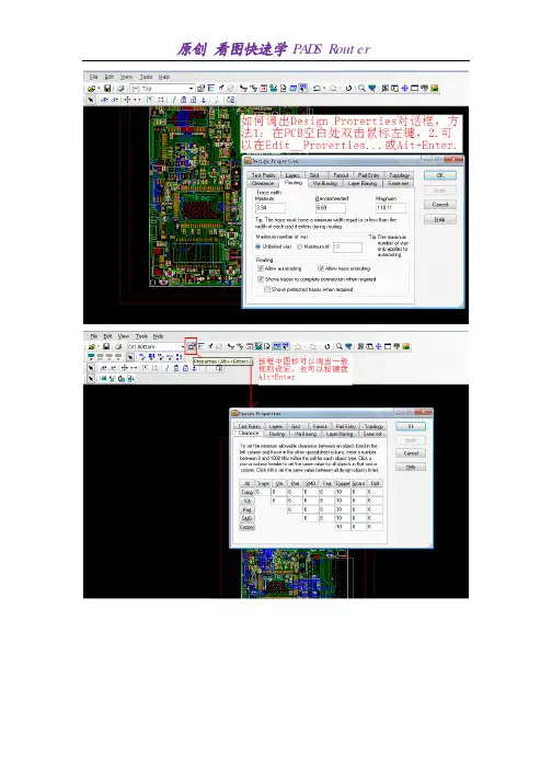
添加蛇形走线添加蛇形走线通常在交互式走线过程中才会用到,在交互式走线过程中鼠标右键选择Add Accordion 。
使用Add Accordion 命令,那么在走线过程中,你每点击一次鼠标左键就添加一个蛇形线段。
还可以通过鼠标在设计中的光标的位置选择来定义蛇形走线以及幅度值。
完成蛇形走线定义后双击鼠标左键回到交互式走线状态。
上图中的红色箭头表示蛇形走线被确定的位置。
定义蛇行走线的起始位置当你开始添加蛇行走线,你有几种方法去定义走线参数。
当你使用默认参数的时候,只要你确定了走线的起始位置,那么随着光标的移动讲自动添加蛇行走线。
你只需在起始位置点击一下鼠标左键。
设置蛇行走线1、选择CLKIN 这个网络,点击鼠标右键选择Unroute 撤消当前的走线。
2、在未选择任何对象状态下鼠标右键选择Select Trace/Pins/Unroutes。
3、在标准工具栏中的层目录中选择Primary Component Side 为当前操作层。
4、右键Interactive Route 或F3 开始对该网络走线。
提示:在增加蛇行走线的时候按Ctrl+L 快捷键查看走线长度。
5、走线过程中在板框开放区域增加一个新的拐角作为蛇行走线的起始点。
6、鼠标右键选择Add Accordion7、在你所需走线方向移动光标,PADS Router 开始按照默认参数来进行蛇行走线。
8、增加你所需要的蛇行走线后双击鼠标左键或鼠标右键选择Complete Accordion 回到交互式走线状态。
9、继续完成走线。
自定义蛇行走线可以通过鼠标选择点来定义蛇行走线参数第一次左键选择走线起始点,第二次确定蛇行线的振幅位置,即可以在走线的过程中改变振幅大小以及蛇行走线的方向。
提示:此时设置的蛇行走线并不影响原先的默认参数。
原创看图快速学PADS Router。
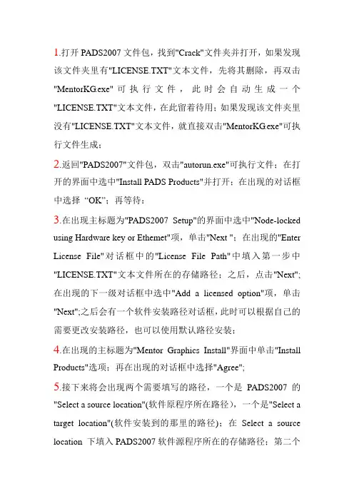
1.打开PADS2007文件包,找到"Crack"文件夹并打开,如果发现该文件夹里有"LICENSE.TXT"文本文件,先将其删除,再双击"MentorKG.exe"可执行文件,此时会自动生成一个"LICENSE.TXT"文本文件,在此留着待用;如果发现该文件夹里没有"LICENSE.TXT"文本文件,就直接双击"MentorKG.exe"可执行文件生成;2.返回"PADS2007"文件包,双击"autorun.exe"可执行文件;在打开的界面中选中"Install PADS Products"并打开;在出现的对话框中选择“OK”;再等待:3.在出现主标题为"PADS2007 Setup"的界面中选中"Node-locked using Hardware key or Ethemet"项,单击"Next ";在出现的"Enter License File"对话框中的''License File Path"中填入第一步中"LICENSE.TXT"文本文件所在的存储路径;之后,点击"Next";在出现的下一级对话框中选中"Add a licensed option"项,单击"Next";之后会有一个软件安装路径对话框,此时可以根据自己的需要更改安装路径,也可以使用默认路径安装;4.在出现的主标题为"Mentor Graphics Install"界面中单击"Install Products"选项;再在出现的对话框中选择"Agree";5.接下来将会出现两个需要填写的路径,一个是PADS2007的"Select a source location"(软件原程序所在路径),一个是"Select a target location"(软件安装到的那里的路径);在Select a source location 下填入PADS2007软件源程序所在的存储路径;第二个Select a target location可以根据自己的需要更改,也可以使用默认路径;之后按"Next";6.在接下来的"Product Selection"中的"Select the product for the chosen platform"中使用默认选项"Windows";在PADS2007文件夹下选择要要安装的文件,一般选择"PADS Layout"、"PADS Logic"、"PADS Router"、"Analog Simulation"、'"Design Exchange"、"HyperLynx V7.7"、"Libraries"项;之后选择"Next";再按"Install";等待;7.在出现的副标题为"Installation Completed"的界面中选择"At a later time"并单击"Done";之后在出现的"Installation Complete"界面下单击"Done"。

PADSRouter⼊门官⽅教程PADS Router TutorialAll rights reserved.This document contains information that is proprietary to Mentor Graphics Corporation. The original recipient of this document may duplicate this document in whole or in part for internal business purposes only, provided that this entire notice appears in all copies. In duplicating any part of this document, the recipient agrees to make every reasonable effort to prevent the unauthorized use and distribution of the proprietary information.This document is for information and instruction purposes. Mentor Graphics reserves the right to make changes in specifications and other information contained in this publication without prior notice, and the reader should, in all cases, consult Mentor Graphics to determine whether any changes have been made.The terms and conditions governing the sale and licensing of Mentor Graphics products are set forth in written agreements between Mentor Graphics and its customers. No representation or other affirmation of fact contained in this publication shall be deemed to be a warranty or give rise to any liability of Mentor Graphics whatsoever.MENTOR GRAPHICS MAKES NO WARRANTY OF ANY KIND WITH REGARD TO THIS MATERIAL INCLUDING, BUT NOT LIMITED TO, THE IMPLIED WARRANTIES OF MERCHANTABILITY AND FITNESS FOR A PARTICULAR PURPOSE.MENTOR GRAPHICS SHALL NOT BE LIABLE FOR ANY INCIDENTAL, INDIRECT, SPECIAL, OR CONSEQUENTIAL DAMAGES WHATSOEVER (INCLUDING BUT NOT LIMITED TO LOST PROFITS) ARISING OUT OF OR RELATED TO THIS PUBLICATION OR THE INFORMATION CONTAINED IN IT, EVEN IF MENTOR GRAPHICS CORPORATION HAS BEEN ADVISED OF THE POSSIBILITY OF SUCH DAMAGES.RESTRICTED RIGHTS LEGEND 03/97U.S. Government Restricted Rights. The SOFTWARE and documentation have been developed entirely at private expense and are commercial computer software provided with restricted rights. Use, duplication or disclosure by the U.S. Government or a U.S. Government subcontractor is subject to the restrictions set forth in the license agreement provided with the software pursuant to DFARS 227.7202- 3(a) or as set forth in subparagraph (c)(1) and (2) of the Commercial Computer Software -Restricted Rights clause at FAR 52.227-19, as applicable.Contractor/manufacturer is:Mentor Graphics Corporation8005 S.W. Boeckman Road, Wilsonville, Oregon 97070-7777.Telephone: 503.685.7000Toll-Free Telephone: 800.592.2210Website: /doc/4f1ac52a2af90242a895e519.htmlSupportNet: /doc/4f1ac52a2af90242a895e519.html /Send Feedback on Documentation: /doc/4f1ac52a2af90242a895e519.html /user/feedback_form.cfm TRADEMARKS: The trademarks, logos and service marks ("Marks") used herein are the property of Mentor Graphics Corporation or other third parties. No one is permitted to use these Marks without the prior written consent of Mentor Graphics or the respective third-party owner. The use herein of a third- party Mark is not an attempt to indicate Mentor Graphics as a source of a product, but is intended to indicate a product from, or associated with, a particular third party. A current list of Mentor Graphics’ trademarks may be viewed at: /doc/4f1ac52a2af90242a895e519.html/terms_conditions/trademarks.cfm.End-User License Agreement: You can print a copy of the End-User License Agreement from:/doc/4f1ac52a2af90242a895e519.html /terms_conditions/enduser.cfm.Table of ContentsLearning the User Interface (1)Assigning Constraints (6)Preparing a Design (10)Placing Components (14)Creating Traces with Interactive Routing (21)Creating High-speed Traces with Interactive Routing (32)Autorouting with PADS Router (51)Checking for Design Rule Violations (58)Learning the User InterfaceThe PADS Router user interface is designed for ease of use and efficiency. PADS Router is designed to meet the needs of the power user, while keeping thebeginner in mind. PADS Router's interface and interaction is similar to otherWindows? applications, including PADS Layout. You can interact with PADSRouter using the keyboard, menus, toolbars, and shortcut menus.In this lesson:y Pointer position displayy Canceling commandsy Shortcut menusy Panning, Zooming, and Scrollingy Selecting objectsPreparationIf it is not already running, start PADS Router and open the file namedpreview.pcb in the \PADS Projects\Samples folder.Pointer position displayPanning, zooming, and scrollingException: If you are using a three button mouse, skip this step.2. Zoom in.y Click and hold the left mouse button in the center of the workspace area you want to magnify.y Exception:If you are using a three-button mouse, click and hold the middle mouse button.y Drag the pointer upward, moving the mouse away from you. A dynamic rectangle attaches to and moves with the pointer. y When the rectangle encompasses the area you want to magnify, release the mouse button to complete the operation. 3. Zoom out. Repeat step 2, but drag the pointer downward, moving the mousetowards you. A stationary rectangle, representing the current workspaceview, appears with a dynamic rectangle, representing the ratio of currentzoom level to new zoom level.4. Practice using Zoom to adjust the magnification.Tip: To reestablish the original view, click the View Board button on thestandard toolbar.5. To end Zoom mode, click the Zoom button on the standard toolbar.Zooming with a mouse wheel buttonTo zoom:1. Press and hold Ctrl.2. Rotate the wheel button up (away from you) to zoom in.3. Rotate the wheel button down (toward you) to zoom out.Changing the zoom level in the navigation windowYou can modify the zoom level of the navigation window while in the workspace.To change the zoom level:1. Point to the center of the design in the workspace and press F5. The zoomlevel increases in the navigation window. Press and hold F5 tozoom smoothly.2. Point to the center of the design in the workspace and press F6. The zoomlevel decreases in the navigation window. Press and hold F6 tozoom smoothly.PanningTo pan:1. Point to the center of the new view.2. Without moving the pointer, press Insert. The area under the pointer in step1 is now the center of the view.Alternative: Click the middle mouse button.Tip: You do not need to be in Zoom mode to pan with a three-button mouse.Smooth scrolling with a three-button mouseTo scroll smoothly, enable the option:1. On the Tools menu, click Options.2. Click the General tab, and in the Pointer Settings area, select the Pandisplay with pointer movements check box.3. Click OK.Result:Move a component or trace to the edge of the screen and the softwareautomatically pans in the pointer direction. Smooth scrolling is also enabled.To scroll smoothly:1. Shift + middle-click.2. Move the pointer in the direction to scroll.Result: A thin white vertex appears, having its first point at the origin of thescroll. The other end of the vertex acts as a scale to determine the speed ofthe scroll. A short line from the apex to the circle results in a smooth scroll.To increase the rate (speed) of scroll, move the pointer away from the circleand stretch the line.Scrolling with a wheel buttonTo scroll vertically:1. Rotate the wheel button up (away from you) to scroll up.2. Rotate the wheel button down (toward you) to scroll down.To scroll horizontally:1. Press and hold Shift.2. Rotate the wheel button up to scroll left.3. Rotate the wheel button down to scroll right.Selecting objects4. Stop cycling when you select the item you want.During designing, you may want to select only specific objects. For example, you may want to select only components. Restrict selections using the Selection Filter toolbar. With the Selection Filter toolbar, you can specify which design objects are selectable. Items turned off in the toolbar cannot be selected.To use the Selection Filter toolbar:1. On the standard toolbar, click the Selection Filter button. The SelectionFilter toolbar appears just below the standard toolbar.2. On the Selection Filter toolbar, click the Anything button to enable selectionof all objects.3. Click the Components button to disable component selection.4. Point to a component outline in the workspace and try to select it. You cannotselect it.5. Point to an object other than a component and select it. You can select otherobjects.6. Press Esc to deselect all objects.Selection shortcutsIf you right-click when no objects are selected, a shortcut menu containing a list of selection shortcuts appears. Clicking one of these shortcuts updates theSelection Filter toolbar to include only the items enabled in the shortcut menu.To use the selection shortcuts:1. With nothing selected, and the Selection Filter toolbar open, right-click andclick Select Nets. Note how the Selection Filter toolbar updates to allow netselection only.2. Right-click again, and click Select Anything. The Selection Filter toolbarupdates to allow selection of any object (except nets, pin pairs, and path,which are always off by default).Selecting all objects of one typeYou can use the Selection Filter toolbar or the selection shortcuts to select allitems of one object type.To select all objects of one type:1. With nothing selected, right-click and click Select Components.2. Right-click again and click Select All to select all the components in thedesign.3. Do not save a copy of the design.You completed the user interface concepts tutorial.Assigning ConstraintsDesign rules include clearance, routing, and high-speed constraints assigned as default restrictions for nets, layers, classes, or pin pairs. In addition, you canassign conditional, differential pair, decal and component rules.In this lesson:y Setting default clearance rulesy Setting default routing rulesy Setting net clearance rulesy Creating a net class rule sety Setting conditional rulesRestrictionThis tutorial requires the General Editing and Extended Rules security options.In PADS Router, click Installed Options on the Help menu to determine whether you can proceed.PreparationIf it is not already running, start PADS Router and open the file namedpreviewnet.pcb in the \PADS Projects\Samples folder.Setting default clearance rulesProperties button > Clearance tabWith PADS Router, you can define the PADS Layout clearance, routing, fanout and pad entry constraints for each level of the design rule hierarchy.The Clearance tab contains a matrix of PCB design data. The matrix lets youspecify values for any or all data types.1. Set a global default clearance value by clicking All in the upper left corner ofthe clearance matrix. A dialog box appears.2. Type 8 and click OK. All matrix values change simultaneously.3. Click the Routing tab. In the Trace Width area, type 6 in the Minimum box,type 8 in the Recommended box, and type 12 in the Maximum box.4. Click the Same net tab. Set a global Same Net default clearance value byclicking All in the upper left corner of the Object clearance matrix. A dialogbox appears.5. Type 12 and click OK. All matrix values change simultaneously.6. To save the changes, click OK in the Design Properties dialog box.Setting default routing rulesProperties button > Layer biasing tabTo avoid routing on the plane layers, remove them from the selected routinglayers as defined in the routing rules. The Layer Biasing tab contains a list ofselected routing layers. This list lets you specify which layers are permitted forrouting.1. Clear the check boxes in the Allow Routing column for the Power Plane layerto prevent routing on the plane layers. The check box for the Ground Planelayer (defined as a CAM plane) may have a check in the box but isautomatically disabled because of its layer status.2. Click OK to close the Design Properties dialog box.Setting net clearance rulesProject Explorer > Object view tabYou can assign net-specific clearances that take precedence over the defaultrules previously entered.1. Double-click on the Net Objects item. Double-click on the Nets item to expandthe tree and show the list of all nets.2. Scroll through the Nets list. Ctrl+click to select nets +5V, +12V, and GND.Right-click and click Properties. The three nets are represented by the NetProperties dialog box.3. Click the Clearance tab, and set a clearance value by clicking All in the upperleft corner of the matrix. A dialog box appears.4. Type 10 as the global clearance and click OK.5. Click the Routing tab. In the Trace Width area, type 10 in the Minimum box,type 12 in the Recommended box, and type 15 in the Maximum box.6. Click OK to close the Net Properties dialog box and save the changes. Setting net clearance rulesSetting conditional rulesPreparing a DesignPrior to a routing session in PADS Router, you can set up your designenvironment for the current session and save the settings for future sessions.In this lesson:y Prerouting proceduresy Changing the color of itemsy Defining a layer pairy Setting the default routing angley Setting a routing grid and a via gridy Enabling real width displayy Setting autopanningy Setting guard bandsy Saving the default settingsPreparationIf it is not already running, start PADS Router and open the file namedpreviewplaced.pcb in the \PADS Projects\Samples folder.Prerouting ProceduresOptions button > Display tabTo improve visibility and reduce screen clutter when you route traces, disable the display of items not required for interactive routing.1. Clear layer check boxes for the Power and Ground plane layers to disable thedisplay of these plane layers.2. Click the background color, black, in the Color selection area.3. Click Background in the general options area to display the backgroundas black.4. In the general options area, click items in the Ref. Des., Keepout, Top Outl,and Bot Outl columns to make these items invisible.5. Click light green in the Color selection area.6. Click Connection in the general options area to display the connections aslight green.7. Leave the Options dialog box open in preparation for the next topic.Tip: With PADS Router you can save color arrangements to reuse them in other designs. After you finish assigning colors to items in the Display tab, you cansave the color arrangement. In the Color scheme area of the Display tab, clickSave as, provide a name for the new color scheme and click OK.Defining a layer pairOptions button > Routing tabDefining a routing layer pair minimizes the amount of time spent on manuallayer changes during interactive routing. Pairing routing layers limits layerchanges to the members of the layer pair. For this four-layer design, the obvious routing pair is made up of the Primary and Secondary Component layers.To define a layer pair:1. In the Layer Pair area, click Primary Component Side in the First layer list,and click Secondary Component Side in the Second layer list.2. Leave the Options dialog box open in preparation for the next topic.Setting the default routing angleOptions button > Routing tabThe trace routing angle setting determines the allowed routing angle (in degrees) of adjacent trace segments as they are introduced during interactive routing.There are three trace routing angle settings:Routing angle Descriptionsegmentsare limited to 45-degree intervals.traceDiagonal Adjacentsegmentsare limited to 90-degree intervals.traceOrthogonal AdjacentAny Angle Adjacent trace segments are not limited to any angle.For the purpose of this tutorial, set the Routing Angle to Orthogonal.1. In the Routing Angle area, click Orthogonal.2. Click OK to close the Options dialog box.Setting a routing grid and a via gridProperties button > Grid tabIn this lesson, use a routing and via grid to facilitate the learning process.Set a routing grid and via grid to 8.33 mils to accommodate the 8 mil trace and 8 mil space requirements of the design as follows:1. Set the X Increment and Y Increment values for the Routing and the Viagrids to 8.33.2. Click OK to save the settings and close the Design Properties dialog box.Otherwise you can use shortcut keys to set the grids.3. Using the Grid shortcut key, type gr 8.33 and press Enter to set theRouting grid.4. Type gv 8.33 and press Enter to set the Via grid.Enabling real width displayOptions button > General tabYou can enable or disable true width display to see trace widths in theirreal width.To set the real width display to 8 mils:1. In the Display settings area, type 8 in the Minimum line width box.2. Click Apply to activate the setting.3. Leave the Options dialog box open in preparation for the next topic.Setting autopanningOptions button > General tabDuring a routing session, it may be convenient to pan around the design. PADS Router contains an autopanning feature that automatically pans the screenfollowing the pointer.To enable autopanning:1. In the Pointer settings area, select the Pan display with pointer movementscheck box to enable the auto-panning feature.2. Click OK to close the Options dialog box.Setting guard bandsOptions button > General tabDuring interactive routing and editing, PADS Router can display guard bands around all objects to indicate clearance boundaries. As the pointer approaches objects, visible outlines appear around nearby objects to indicate the clearance boundaries for rules in effect for the current operation.To turn guard bands on:1. In the Display settings area, select the Show guard bands on objectcheck box.2. Click OK to apply the setting and close the Options dialog box.3. Do not save a copy of the design.You completed the prerouting procedures tutorial.Placing ComponentsPADS Router contains many commands for editing component placement withina design.In this lesson:y Placement toolbary Setting the move originy Preplacement proceduresy Placing components using movey Placing components using the Object View taby Experimenting with placement toolsy Changing placement propertiesRestrictiony This tutorial requires the DFF Audit, General Editing and Dynamic Route Editing security options. In PADS Router, click Installed Options on the Helpmenu to determine whether you can proceed.PreparationIf it is not already running, start PADS Router and open the file namedpreviewrules.pcb in the \PADS Projects\Samples folder.Placement toolbarSetting the move originOptions button > General tabPADS Router enables you to choose between three origins for moving objects.These origins include:Origin LocationBy Cursor Location The location of the pointer at the time you initiate acomponent move.By Origin The actual component origin as defined in the PCB.By Mid-Point The center of the component, calculated by finding thecenter point of a rectangular box that encompasses the partoutline and its pins.For the purpose of the exercises below, you will set the move-by mode to Move By Origin.To set the move origin:1. In the Object movement area, click Origin in the Move object by list.2. In the Drag object using list, make sure that Drag and attach is selected.3. Click OK to apply the changes and close the Options dialog box.Changing placement properties5. Experiment with changing the orientation or location of a few componentsusing the Component Properties tab.6. When finished, click OK to close the Component Properties dialog box.7. Do not save a copy of the file.Preplacement proceduresView menu > NetsTo aid in the placement and correct orientation of decoupling capacitors, assign a color to the +5V net.1. In the Net list, expand Net Objects.2. Expand the Nets branch.3. In the Nets list, click +5V.4. Click Add to add +5V to the View details area.5. In the View details area, click +5V.6. Click dark gray in the Palette and then click on the Colors of Pads, Vias,Unroutes box to display all component pins and vias connected to +5V asdark gray.。
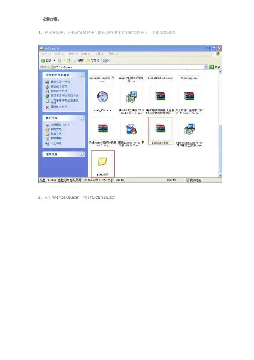
安装步骤:
1、解压安装包,经验证安装包不可解压到有中文名字的文件夹下,否则安装出错。
2、运行“MentorKG.exe”,得到“LICENSE.txt”
3、双击“msi_setup.exe”安装,出现第4步安装界面。
4、点击第一项,进入第5步。
5、点击“Agree”
6、默认即可,点击“NEXT”.
7、选择安装组件(根据个人需要)
8、点击“Install”安装,出现第9步界面
9、安装过程比较费时
10、安装过程中,弹出下图对话框,选择第三项“At a later time”后,点击“Done”
11、当出现下图界面后,点击“Done”,程序安装完成。
12、关闭安装界面。
13、破解,将第2步生成的“LICENSE.txt”改为“LICENSE.dat”
14、在C盘根目录下新建“Flexlm”文件夹,然后将13步的“LICENSE.dat”放入其中,如下图。
至此,PADS2007安装完成。
15、下面两图,为PADS Layout和PADS Logic的工作界面。

PADSRouterPADS点睛(2008-07-08 19:08:43)转载标签:杂谈分类:技术杂谈Power PCB 设计复用(以PADS 2005为例)建立一个设计复用(*.reu文件)1.选择要设计的对象2.右键,弹出菜单中选Make Reuse,可以看后面的选择和未选择报告(Selection deselection)3.输入Reuse的文件名4.选取Save to file5.保存该文件到文件夹以备后用在以下学习中,所有的应用环境必须在ECO下,关闭设计规则检查(可用DRO命令)增加一个设计复用1.在菜单中单击Add Reuse,弹出对话框2.选择要增加的复用文件,弹出“Reuse Properties 对话框3.如已经存在一个复用文件,则弹出一个提示,“确定”增加一个副本,“否则”取消4. “Reuse Properties 对话框中,点”Net Properties”看是否有网络冲突,如果有需要合并的网络,必须在ECO下手动合并5. 如果没有错误,将出现一个如下提示对话框6.完成增加设计复用。
编辑设计复用1.打开要编辑的设计复用(文件类型选*.reu),根椐需要编辑它或者在右键弹出菜单中选择Break Reuse取消设计复用。
2.编辑完成后,将选择类型定为“select Reuse”,右键,Save to file,覆盖掉以前的文件,提示:是否覆盖XXX文件,选“Yes",完成!建立原点座标:(用PADS 2005 打开没有layout BGA文件)1.鼠标右键,点选"Select Traces/Pins",再点BGA的左上角的一个PAD2.以这个PAD建立原点座标,Setup/origin.选择BGA FANOUT的层:Setup/Layers Setup,BGA一般放在TOP Component 层,Plane Typet选No Plane ,Routing 选 Any.然后“OK”。

PADS2007系列教程――PADS Logic (原PowerLogic)PADS Logic 教程PADS Logic教程简介欢迎使用PADS Logic 教程。
本教程由比思电子有限公司(KGS Technology Ltd.)编写,本公司是Mentor (以前的Innoveda-PADS) PADS(以前的PowerPCB)产品、APLAC 的射频和微波仿真工具、DpS 的电气图CAD 系统PCschematic在中国的授权代理商。
KGS 公司自1989 年开始,一直致力于PADS 软件产品的销售和支持。
公司提供电子产品在原理样机设计开发阶段全面的解决方案。
包括相关的CAE/CAD/CAM 等EDA 软件、提供PCB 设计服务、PCB 样板加工制造、快速PCB 加工设备、PCB 元器件装配。
所有技术人员都具有十年以上的PCB 设计领域从业经历。
本教程描述了PADS Logic 的各种功能和特点、以及使用方法。
这些功能包括:·如何在PADS Logic 中使用工作区(Working Area)。
·如何在PADS Logic 的元件库中定义目标库(Library)。
·如何从库中搜索有关的元件(Part)。
·如何添加连线(Connection)、总线(Bus)、使用页间连接符号(Off-Page)。
·移动(Move)、拷贝(Copy)、删除(Delete)和编辑(Edit)等操作方式(Mode)。
·在设计数据编辑时使用查询/修改(Query/Modify)命令。
·如何定义设计规则(Design Rules)。
·如何建立网表(Netlist)和SPICE 格式网络表以及材料清单(BOM)报告和生成智能PDF 文档。
·如何输入中英文文本和输入变量数值。
·如何使用目标连接与嵌入(OLE)功能。
·如何使用工程设计更改(Engineering Change Orders (ECO))。
Pads2007软件用法PCB画图技术 2009-10-12 11:10 阅读242 评论0 字号:大大中中小小1:PADS新手的一点心得和技巧偶是PADS的新手,原来一直用protel。
花了四天时间第一次用PADS2005画了一块大板子,开始确实有很多感觉不方便不熟悉的地方。
现在算是入门了,也总结了一些经验和技巧。
希望对PADS的新手能有所帮助。
1.布局时飞线(鼠线,connection)的处理。
Layout的缺省设置并不是让飞线最短化。
一开始布元件时,飞线实在是密如蛛网,晕头转向。
Tools\length minimization (CRTL+M) 也没有用,硬着头皮在缺省设置下完成了元件布局。
几欲faint。
后来才发现其实没有设置好。
正确或者说方便的设置应该是让飞线最短并且在移动中始终最短。
Setup\design rules\default rules\routing\ topology type\minimize这样在按CTRL+M,很多飞线就消失了,也就最短了Setup\preference\length minimize\during moving这样移动元件是飞线始终最短。
另外,很多飞线其实是地线。
可以把地线的飞线先hide起来。
并把地线的net设置成比较特殊的颜色。
这样就布局就方便多了。
View\nets\ 选在左边net list 选GND net,加到右边view list。
在右边选GND,下面view unroute details 选none,在左边颜色中选一个颜色。
这样地线的飞线就hide起来了,并且是同一种颜色。
当然这里要小心信号地和power地要分开先。
这样的设置布局起来就方便多了。
早知道就好,ft。
2.改全部元件的字体属性。
和protel一样,这个是可以一次全部改成相同的属性的。
单击鼠标右键,选select components, 再单击右键,选 select all (CTRL+A)。
PADS 2007 教程简介PADS 2007是一种电子设计自动化(EDA)软件,用于进行PCB(Printed Circuit Board)设计和布局。
它是一款功能强大且易于使用的工具,可以帮助工程师们快速而精确地设计印刷电路板。
在这个教程中,我们将带您了解PADS 2007的基本知识,并进行一些实际的操作示范,帮助您快速上手和掌握该软件的使用方法。
环境设置在开始PADS 2007之前,确保您的电脑符合以下最低要求:•操作系统:Windows XP或更高版本•内存:至少2GB•硬盘空间:至少2GB•屏幕分辨率:1024x768或更高分辨率完成硬件要求后,您需要下载和安装PADS 2007软件。
请注意,PADS 2007是一款商业软件,需要购买许可证才能使用。
创建新工程在PADS 2007中,我们可以创建一个新的工程来进行PCB 设计和布局。
下面是创建新工程的步骤:1.启动PADS 2007软件,并选择“File” > “NewProject”。
2.输入工程名称和保存路径,并选择一个设计模板(如果有)。
3.点击“Next”并按照向导的指示完成创建工程的过程。
PCB布局设计一旦创建了新工程,我们就可以开始进行PCB布局设计。
以下是一些基本的布局设计步骤:1.绘制板卡轮廓:在PCB编辑器中,使用绘图工具绘制PCB的轮廓。
这将决定PCB的尺寸和外形。
2.定位组件:将所需的元件(IC、电阻、电容等)拖放到PCB编辑器中,根据需要进行定位和旋转。
3.连接器布局:根据电路原理图,将连接器放置到合适的位置上,确保与其他元件的连线正确连接。
4.连线布线:使用布线工具将组件之间的连线进行布线。
5.添加电源和地线:将电源和地线引导到适当的位置,确保电源供应的稳定性和地线的良好连接。
6.规划布局:对PCB进行规划,确保元件和连线之间有足够的间距,以避免干扰和短路。
信号完整性和电磁兼容性在设计PCB时,我们需要考虑信号完整性和电磁兼容性。

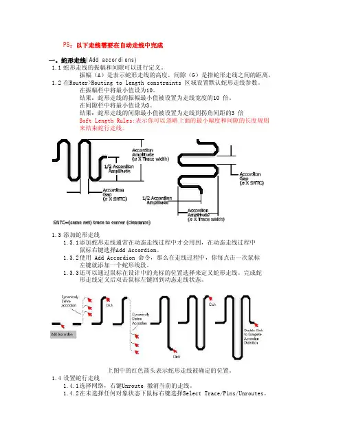
PS:以下走线需要在自动走线中完成一。
蛇形走线(Add accordions)1.1蛇形走线的振幅和间隙可以进行定义。
振幅(A)是表示蛇形走线的高度,间隙(G)是指蛇形走线之间的距离。
1.2在Router>Routing to length constraints 区域设置默认蛇形走线参数。
在振幅栏中将最小值设为10。
结果:蛇形走线的振幅最小值被设置为走线宽度的10 倍。
在间隙栏中将最小值设为3。
结果:蛇形走线的间隙最小值被设置为走线到拐角间距的3 倍Soft Length Rules:表示你可以忽略上面的最小幅度和间隙的长度规则来结束蛇行走线。
1.3添加蛇形走线1.3.1添加蛇形走线通常在动态走线过程中才会用到,在动态走线过程中鼠标右键选择Add Accordion。
1.3.2使用 Add Accordion 命令,那么在走线过程中,你每点击一次鼠标左键就添加一个蛇形线段。
1.3.3还可以通过鼠标在设计中的光标的位置选择来定义蛇形走线。
完成蛇形走线定义后双击鼠标左键回到动态走线状态。
上图中的红色箭头表示蛇形走线被确定的位置。
1.4设置蛇行走线1.4.1选择网络,右键Unroute 撤消当前的走线。
1.4.2在未选择任何对象状态下鼠标右键选择Select Trace/Pins/Unroutes。
1.4.3在标准工具栏中的层目录中选择要走线层为当前操作层。
1.4.4右键Interactive Route 或F3 开始对该网络走线。
1.4.5走线过程中在板框开放区域增加一个新的拐角作为蛇行走线的起始点。
1.4.6鼠标右键选择Add Accordion。
1.4.7在你所需走线方向移动光标,开始按照默认参数来进行蛇行走线。
1.4.8增加你所需要的蛇行走线后双击鼠标左键或鼠标右键选择CompleteAccordion 回到动态走线状态。
1.4.9继续完成走线。
1.5自定义蛇行走线可以通过鼠标选择点来定义蛇行走线参数:第一次左键选择走线起始点,第二次确定蛇行线的振幅位置。
PADS 2007 学习目录一、PADS显示地....................................................................................................................... - 2 -二、PADS开窗........................................................................................................................... - 3 -三、规则检查.............................................................................................................................. - 7 -四、蛇形走线及删除.................................................................................................................. - 9 -五、GERBER文件的生成....................................................................................................... - 12 -六、不同PCB板的位置定位复制粘贴 .................................................................................. - 20 -七、同PCB板的位置定位 ...................................................................................................... - 21 -八、PCB同属性值元件的选定 ............................................................................................... - 23 -九、PCB生成BOM ................................................................................................................. - 24 -十、PCB生成图纸 ................................................................................................................... - 38 - 十一、PCB生成贴片程序 ....................................................................................................... - 43 -一、PADS显示地1.快捷命令:PO2.显示成片地:Tools Pour Manager3.选:Hatch选项卡选Start执行地框图二、PADS开窗快捷键:无1.先打开Drafting Toolbar工具2.选择所需要的开窗层Solder Mask Top顶层阻焊层3.选择好层之后,在Drafting Toolbar工具盒中的Copper工具。
首先你一定有PADS安装程序了,把它放在C盘以外的盘,当然你也可以放C盘,那样会对电脑系统有一定影响。
把它解压,然后在下载一个虚拟光驱,在网上找这个DTLITE4402虚拟光驱下载,10M左右,这个不错!其他的虚拟光驱也可以。
安装以后在设置一下光驱支持格式,重新启动电脑加载。
现在你的PADS2007,已经被安装了的虚拟光驱识别,变成这个图标了,呵呵!第二步:在解压的文件夹里面拷贝复制Crack文件夹到本地磁盘目录*:C\第三步:在C盘打开CRACK,运行MentorKG.exe文件生成License.txt 文件双击这个图标,就可以出现下面安装界面了:点第四项: Install License Server 先安装生成License.Dat许可文件!选第一项 Typical典型安装方式,然后“Next”… …运行刚刚MentorKG.exe 文件生成License.txt 文件”的位置,然后一直Next...“Next”… …将会在目录C:\Flexlm 下生成License.dat 文件License.dat 文件安装完成!再回到安装主菜单,点第一项安装Install PADS Products… …关闭杀毒软件和防火墙!点“OK”… …稍等几秒弹出检查选择第三项,然后“Next”… …装完后先别运行安装完软件后再安装 License 文件选择日常工作文件存放目录PADS Projects,点击“Next”… …安装程序会自动弹出一些窗口,不于理睬等待安装窗口弹出选择第一项开始安装软件,点“Install Products”… …点“Agree”同意许可协议… …继续NEXT“Select a source location:”选择软件安装源路径,“Select a target location:”选择安装软件到电脑的路径,然后“Next”… …选择想要安装的组件,在PADS LAYOUT,PADS LOGIC,PADS ROUTER打钩,只安装常用组件要400M 左右,然后“Next”… …“Install”开始安装… …需要10分钟的样子。
a。
PADS2007中文教程1111-—-—PADS2007_教程-PADS Logic。
pdf 2222————PADS2007_教程-PADS Layout。
pdf 3333--—-PADS2007_教程-PADS Router。
pdf 4444——-—PADS2007_教程-高级封装设计.pdf1、PAGE UP/PAGE DOWN为视图的放大与缩小//1111----按住CTRL键,滑动鼠标的滑轮,就可以起到放大与缩小的功能,这样也可以省去去按右边的小键盘2、原理图的标框可以自己去画,这样可以一张图可以显示更多的内容--—SHEET尺寸大小也可以选择,常用A3大小3、可以自己建立自己的PART TYPE库,这样跟系统自带可以分开,自己也好查找4、增加OFF-PAGE连接的时候,可以设置对应的页码是显示还是隐藏5、建立一个PART TYPE的顺序为-—-—先建立CAE DECAL,然后是创建PART TYPE 来引用刚才的CAE DECAL6、可以新建自己的PIN DECAL,并在画CAE DECAL引用它7、增加文字与文字变量8、无模命令模式的显示—-—-直接按键盘字母,退出按ESC键9、显示网格的设置—-—-—设置可见网格的大小,方便元器件对齐放置 10、文字字体跟线宽设置11、多个SHEET建立与管理-———-方便原理图成模块化/功能块化放置12、增加总线及总线的编辑与连接13、原理图打印成PDF,打印成智能化PDF14、左边的各种类型列表————-封装,网络连接,元器件等等15、Display Color控制各层的显示与颜色设置16、ECO工程更改在LAYOUT跟LOGIC之间17、LAYOUT怎么画板的外形18、LAYOUT怎么导入网表—---直接从ASC文件导入,从LOGIC发送过去19、LAYOUT的走线怎么显示出来20、定义层——-—信号/厚度21、定义设计规则22、inch,mil,mm之间的换算关系 1mil=1/1000inch=0.00254cm=0.0254mm1inch=1000mil=2。
pads route基本操作Pads Route基本操作Pads Route是一款广泛使用的PCB设计软件,它提供了一系列强大的功能来帮助工程师设计和布局印制电路板。
本文将介绍Pads Route的基本操作,帮助初学者快速上手。
一、创建布局1. 打开Pads Route软件,点击菜单栏中的“File”选项,选择“New”来创建一个新的工程。
2. 在弹出的对话框中,选择工程的名称和路径,并设置板层的数量和尺寸。
3. 确定设置后,点击“OK”按钮,Pads Route将自动创建一个空的布局文件供你进行设计。
二、导入元件1. 点击菜单栏中的“Library”选项,选择“Import Part”来导入元件库。
2. 在弹出的对话框中,选择要导入的元件库文件,并点击“Open”按钮。
3. 导入完成后,你可以在元件库中找到你所需的元件。
三、放置元件1. 点击工具栏中的“Place”按钮,选择要放置的元件。
2. 将鼠标移动到布局界面上,你会看到一个元件的图标跟随鼠标移动。
3. 点击鼠标左键,将元件放置在合适的位置上。
4. 重复以上步骤,直到所有的元件都被放置在布局中。
四、连接元件1. 点击工具栏中的“Route”按钮,选择要连接的元件。
2. 将鼠标移动到一个元件的引脚上,你会看到一个连接线的图标跟随鼠标移动。
3. 点击鼠标左键,连接线将从该引脚开始。
4. 将鼠标移动到另一个元件的引脚上,点击鼠标左键,连接线将连接到该引脚。
5. 重复以上步骤,直到所有的元件被正确连接起来。
五、布线1. 点击工具栏中的“Route”按钮,选择要布线的元件。
2. 将鼠标移动到一个连接线上,你会看到一个布线的图标跟随鼠标移动。
3. 点击鼠标左键,布线开始。
4. 将鼠标移动到需要布线的路径上,点击鼠标左键,布线将沿着该路径进行。
5. 重复以上步骤,直到所有的连接线都被正确布线。
六、调整布局1. 点击工具栏中的“Move”按钮,选择要调整的元件或连接线。