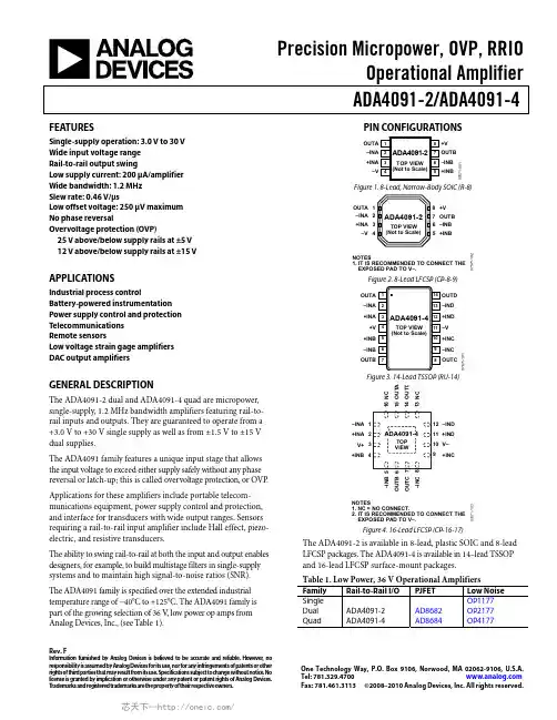
ADA4091-2_4091-4
- 格式:pdf
- 大小:543.32 KB
- 文档页数:20
Precision Micropower, OVP, RRIOOperational Amplifier Data Sheet ADA4091-2/ADA4091-4Rev. H Document FeedbackInformation furnished by Analog Devices is believed to be accurate and reliable. However, noresponsibility is assumed by Analog Devices for its use, nor for any infringements of patents or other rights of third parties that may result from its use. Specifications subject to change without notice. No license is granted by implication or otherwise under any patent or patent rights of Analog Devices. T rademarks and registered trademarks are the property of their respective owners. O ne Technology Way, P.O. Box 9106, Norwood, MA 02062-9106, U.S.A. Tel: 781.329.4700 ©2008–2016 Analog Devices, Inc. All rights reserved. Technical Support FEATURESSingle-supply operation: 3.0 V to 30 VWide input voltage rangeRail-to-rail output swingLow supply current: 200 μA/amplifierWide bandwidth: 1.2 MHzSlew rate: 0.46 V/μsLow offset voltage: 250 μV maximumNo phase reversalOvervoltage protection (OVP)25 V above/below supply rails at ±5 V12 V above/below supply rails at ±15 V APPLICATIONSIndustrial process controlBattery-powered instrumentationPower supply control and protection TelecommunicationsRemote sensorsLow voltage strain gage amplifiersDAC output amplifiersGENERAL DESCRIPTIONThe ADA4091-2 dual and ADA4091-4 quad are micropower, single-supply, 1.2 MHz bandwidth amplifiers featuring rail-to-rail inputs and outputs. They are guaranteed to operate from a +3.0 V to +30 V single supply as well as from ±1.5 V to ±15 V dual supplies.The ADA4091-2/ADA4091-4 features a unique input stage that allows the input voltage to exceed either supply safely without any phase reversal or latch-up; this is called overvoltage protection (OVP).Applications for these amplifiers include portable telecom-munications equipment, power supply control and protection, and interface for transducers with wide output ranges. Sensors requiring a rail-to-rail input amplifier include Hall effect, piezo-electric, and resistive transducers.The ability to swing rail-to-rail at both the input and output enables designers, for example, to build multistage filters in single-supply systems and to maintain high signal-to-noise ratios (SNR). The ADA4091-2/ADA4091-4 is specified over the extended indus-trial temperature range of −40°C to +125°C. The ADA4091-2/ ADA4091-4 is part of the growing selection of 36 V, low power operational amplifiers from Analog Devices, Inc., (see Table 1).PIN CONFIGURATIONSOUTA1–INA2+INA3–V4+V8OUTB7–INB6+INB5ADA4091-2TOP VIEW(Not to Scale)7671-1Figure 1. 8-Lead, Narrow-Body SOIC (R-8)NOTES1. IT IS RECOMMENDED TO CONNECT THEEXPOSED PADTO V–.07571-12+INA–VOUTA–INA–INB+INB+VOUTBFigure 2. 8-Lead LFCSP (CP-8-21)7671-11–INA+INA+VOUTB–INB+INBOUTA–IND+IND–VOUTC–INC+INCOUTDFigure 3. 14-Lead TSSOP (RU-14)7671-13121110–IND+INDV–9+INC–INAV++INA+INB6OUTB5–INB7OUTC8–INC16NC15OUTA14OUTD13NCNOTES1.NC = NO CONNECT.2. IT IS RECOMMENDED TO CONNECT THEEXPOSED PAD TO V–.Figure 4. 16-Lead LFCSP (CP-16-17)The ADA4091-2 is available in 8-lead, plastic SOIC and 8-lead LFCSP packages. The ADA4091-4 is available in 14–lead TSSOPand 16-lead LFCSP surface-mount packages.Table 1. Low Power, 36 V Operational AmplifiersFamily Rail-to-Rail I/O PJFET Low NoiseSingle OP1177 Dual ADA4091-2AD8682 OP2177Quad ADA4091-4AD8684 OP4177ADA4091-2/ADA4091-4Data SheetRev. H | Page 2 of 20TABLE OF CONTENTSFeatures .............................................................................................. 1 Applications ....................................................................................... 1 General Description ......................................................................... 1 Pin Configurations ........................................................................... 1 Revision History ............................................................................... 2 Specifications ..................................................................................... 3 Electrical Specifications ............................................................... 3 Absolute Maximum Ratings ............................................................ 6 Thermal Resistance ...................................................................... 6 ESD Caution...................................................................................6 Typical Performance Characteristics ..............................................7 Theory of Operation ...................................................................... 14 Input Stage ................................................................................... 14 Output Stage ................................................................................ 14 Input Overvoltage Protection ................................................... 15 Outline Dimensions ....................................................................... 16 Ordering Guide .. (18)REVISION HISTORY5/2016—Rev. G. to Rev. HChanged CP-8-9 to CP-8-21 ........................................ Throughout Changes to Figure 2 .......................................................................... 1 Updated Outline Dimensions ....................................................... 16 Changes to Ordering Guide . (18)10/2013—Rev. F. to Rev. GChanged Open-Loop Impedance to Closed-Loop Impedance (Throughout) .................................................................................... 3 Updated Outline Dimensions . (17)10/2010—Rev. E. to Rev. FChanges to Features Section and General Description Section . 1 Changes to Outline Dimensions (17)5/2010—Rev. D. to Rev. EChanges to Data Sheet Title ............................................................ 1 Changes to Table 2, Input Characteristics, Offset Voltage .......... 3 Changes to Table 3, Input Characteristics, Offset Voltage .......... 4 Changes to Table 4, Input Characteristics, Offset Voltage . (5)4/2010—Rev. C to Rev. DChanges to Table 2, Added LFCSP to Input Characteristics ...... 3 Changes to Table 3, Added LFCSP to Input Characteristics ...... 4 Changes to Table 4, Added LFCSP to Input Characteristics (5)10/2009—Rev. B to Rev. CAdded 8-Lead LFCSP and 16-Lead LFCSP ..................... U niversal Change to Features Section ............................................................. 1 Updated Outline Dimensions ....................................................... 16 Changes to Ordering Guide .......................................................... 18 7/2009—Rev. A to Rev. BAdded New Part ADA4091-4 ........................................... U niversal Changes to Features Section, General Description Section, and Figure 4 ............................................................................................... 1 Added Figure 2, Renumbered Sequentially ................................... 1 Changes to Table 1 ............................................................................. 1 Changes to Table 2 ............................................................................. 3 Changes to Table 3 ............................................................................. 4 Changes to Table 4 ............................................................................. 5 Changes to Table 5 ............................................................................. 6 Changes to Table 6 ............................................................................. 6 Updated Outline Dimensions ....................................................... 16 Changes to Ordering Guide . (16)7/2009—Rev. 0 to Rev. AChanges to Data Sheet Title ............................................................. 1 Changes to Features .......................................................................... 1 Changes to Table 2 ............................................................................. 3 Changes to Table 3 ............................................................................. 4 Changes to Table 4 ............................................................................. 5 Added Input Current Parameter, Table 5 ....................................... 6 Added New Figure 12 and Figure 13, RenumberedSequentially ........................................................................................ 8 Added New Figure 24 and Figure 25 ........................................... 10 Added New Figure 36 and Figure 37 ........................................... 12 Added New Figure 43 .................................................................... 13 Changes to Input Overvoltage Protection Section..................... 15 Changes to Ordering Guide . (16)10/2008—Revision 0: Initial VersionData Sheet ADA4091-2/ADA4091-4 SPECIFICATIONSELECTRICAL SPECIFICATIONSV SY = ±1.5 V, V CM = 0.0 V, T A = 25°C, unless otherwise noted.Table 2.Parameter Symbol Test Conditions/Comments Min Typ Max Unit INPUT CHARACTERISTICSOffset Voltage V OS−250 −40 +250 µVADA4091-4 LFCSP package −400 −40 +400 µV−40°C ≤ T A ≤ +125°C −600 +600 µV Offset Voltage Drift ∆V OS/∆T 2.5 µV/°C Input Bias Current I B−55 −44 nA−40°C ≤ T A ≤ +85°C −55 +55 nA−40°C ≤ T A ≤ +125°C −275 +275 nAInput Offset Current I OS−3 0.5 +3 nA−40°C ≤ T A ≤ +85°C −5 +5 nA−40°C ≤ T A ≤ +125°C −75 +75 nAInput Voltage Range −1.5 +1.5 V Common-Mode Rejection Ratio CMRR V CM = −1.35 V to +1.35 V 84 100 dB−40°C ≤ T A ≤ +125°C 78 dB Large Signal Voltage Gain A VO R L = 100 kΩ, V O = −1.2 V to +1.2 V 106 113 dB−40°C ≤ T A ≤ +125°C 101 dBR L = 10 kΩ, V O = −1.2 V to +1.2 V 92 94 dB−40°C ≤ T A ≤ +125°C 85 dB OUTPUT CHARACTERISTICSOutput Voltage High V OH R L = 100 kΩ to GND 1.490 1.495 V−40°C ≤ T A ≤ +125°C 1.490 VR L = 10 kΩ to GND 1.475 1.485 V−40°C to +125°C 1.455 V Output Voltage Low V OL R L = 100 kΩ to GND −1.499 −1.495 V−40°C ≤ T A ≤ +125°C −1.495 VR L = 10 kΩ to GND −1.495 −1.490 V−40°C ≤ T A ≤ +125°C −1.490 VShort-Circuit Limit I SC Source/sink ±31 mA Closed-Loop Impedance Z OUT f = 1 MHz, A V = 1 102 Ω POWER SUPPLYPower Supply Rejection Ratio PSRR V SY = 2.7 V to 36 V 108 126 dB−40°C ≤ T A ≤ +125°C 100 dB Supply Current per Amplifier I SY I O = 0 mA 165 200 µA−40°C ≤ T A ≤ +125°C 300 µA DYNAMIC PERFORMANCESlew Rate SR R L = 100 kΩ, C L = 30 pF 0.46 V/µs Settling Time t S To 0.01% 22 µsGain Bandwidth Product GBP 1.22 MHz Phase Margin ΦM69 Degrees NOISE PERFORMANCEVoltage Noise e n p-p 0.1 Hz to 10 Hz 0.8 µV p-p Voltage Noise Density e n f = 1 kHz 24 nV/√HzRev. H | Page 3 of 20ADA4091-2/ADA4091-4 Data Sheet V SY = ±5.0 V, V CM = 0.0 V, T A = 25°C, unless otherwise noted.Table 3.Parameter Symbol Test Conditions/Comments Min Typ Max Unit INPUT CHARACTERISTICSOffset Voltage V OS−250 −45 +250 µVADA4091-4 LFCSP package −400 −40 +400 µV−40°C ≤ T A ≤ +125°C −600 +600 µVOffset Voltage Drift ∆V OS/∆T 2.5 µV/°C Input Bias Current I B−60 −50 nA−40°C ≤ T A ≤ +85°C −80 +80 nA−40°C ≤ T A ≤ +125°C −350 +350 nAInput Offset Current I OS−3 0.5 +3 nA−40°C ≤ T A ≤ +85°C −7 +7 nA−40°C ≤ T A ≤ +125°C −100 +100 nAInput Voltage Range −5 +5 V Common-Mode Rejection Ratio CMRR V CM = −4.85 V to +4.85 V 95 113 dB−40°C ≤ T A ≤ +125°C 88 dB Large Signal Voltage Gain A VO R L = 100 kΩ, V O = ±4.7 V 113 117 dB−40°C ≤ T A ≤ +125°C 106 dBR L = 10 kΩ, V O = ±4.7 V 98 100 dB−40°C ≤ T A ≤ +125°C 90 dB OUTPUT CHARACTERISTICSOutput Voltage High V OH R L = 100 kΩ to GND 4.980 4.990 V−40°C ≤ T A ≤ +125°C 4.980 VR L = 10 kΩ to GND 4.950 4.960 V−40°C ≤ T A ≤ +125°C 4.900 V Output Voltage Low V OL R L = 100 kΩ to GND −4.998 −4.990 V−40°C ≤ T A ≤ +125°C −4.980 VR L = 10 kΩ to GND −4.990 −4.980 V−40°C ≤ T A ≤ +125°C −4.975 VShort-Circuit Limit I SC Source/sink ±20 mA Closed-Loop Impedance Z OUT f = 1 MHz, A V = 1 77 Ω POWER SUPPLYPower Supply Rejection Ratio PSRR V SY = 2.7 V to 36 V 108 126 dB−40°C ≤ T A ≤ +125°C 100 dB Supply Current per Amplifier I SY I O = 0 mA 180 225 µA−40°C ≤ T A ≤ +125°C 300 µA DYNAMIC PERFORMANCESlew Rate SR R L = 100 kΩ, C L = 30 pF 0.46 V/µs Settling Time t S To 0.01% 22 µsGain Bandwidth Product GBP 1.22 MHz Phase Margin ΦM70 Degrees NOISE PERFORMANCEVoltage Noise e n p-p 0.1 Hz to 10 Hz 0.8 µV p-p Voltage Noise Density e n f = 1 kHz 24 nV/√HzRev. H | Page 4 of 20Data Sheet ADA4091-2/ADA4091-4 V SY = ±15.0 V, V CM = 0.0 V, V O = 0.0 V, T A = 25°C, unless otherwise noted.Table 4.Parameter Symbol Test Conditions/Comments Min Typ Max Unit INPUT CHARACTERISTICSOffset Voltage V OS−250 −35 +250 µVADA4091-4 LFCSP package −400 −40 +400 µV−40°C ≤ T A ≤ +125°C −600 +600 µV Offset Voltage Drift ∆V OS/∆T 3.0 µV/°C Input Bias Current I B−60 −50 nA−40°C ≤ T A ≤ +85°C −80 +80 nA−40°C ≤ T A ≤ +125°C −510 +510 nAInput Offset Current I OS−3 0.5 +3 nA−40°C ≤ T A ≤ +85°C −10 +10 nA−40°C ≤ T A ≤ +125°C −140 +140 nAInput Voltage Range −15 +15 V Common-Mode Rejection Ratio CMRR V CM = −14.85 V to +14.85 V 104 121 dB−40°C ≤ T A ≤ +125°C 95 dB Large Signal Voltage Gain A VO R L = 100 kΩ, V O = ±14.7 V 116 119 dB−40°C ≤ T A ≤ +125°C 108 dBR L = 10 kΩ, V O = ±14.7 V 102 104 dB−40°C ≤ T A ≤ +125°C 93 dB OUTPUT CHARACTERISTICSOutput Voltage High V OH R L = 100 kΩ to GND 14.975 14.980 V−40°C ≤ T A ≤ +125°C 14.950 VR L = 10 kΩ to GND 14.900 14.920 V−40°C ≤ T A ≤ +125°C 14.800 V Output Voltage Low V OL R L = 100 kΩ to GND −14.996 −14.990 V−40°C ≤ T A ≤ +125°C −14.985 VR L = 10 kΩ to GND −14.975 −14.950 V−40°C ≤ T A ≤ +125°C −14.940 VShort-Circuit Limit I SC Source/sink ±20 mA Closed-Loop Impedance Z OUT f = 1 MHz, A V = 1 71 Ω POWER SUPPLYPower Supply Rejection Ratio PSRR V SY = 2.7 V to 36 V 108 126 dB−40°C ≤ T A ≤ +125°C 100 dB Supply Current per Amplifier I SY I O = 0 mA 200 250 µA−40°C ≤ T A ≤ +125°C 350 µA DYNAMIC PERFORMANCESlew Rate SR R L = 100 kΩ, C L = 30 pF 0.46 V/µs Settling Time t S To 0.01% 22 µsGain Bandwidth Product GBP 1.27 MHz Phase Margin ΦM72 Degrees Channel Separation CS f = 1 kHz 100 dB NOISE PERFORMANCEVoltage Noise e n p-p 0.1 Hz to 10 Hz 0.8 µV p-p Voltage Noise Density e n f = 1 kHz 25 nV/√HzRev. H | Page 5 of 20ADA4091-2/ADA4091-4Data SheetRev. H | Page 6 of 20ABSOLUTE MAXIMUM RATINGSTable 5.Parameter Rating Supply Voltage 36 VInput VoltageRefer to the InputOvervoltage Protection section Differential Input Voltage 1 ±V SY Input Current±5 mA Output Short-Circuit Duration to GND IndefiniteStorage Temperature Range −65°C to +150°C Operating Temperature Range −40°C to +125°C Junction Temperature Range−65°C to +150°C Lead Temperature (Soldering, 60 sec)300°C1Input current must be limited to ±5 mA.Stresses at or above those listed under Absolute Maximum Ratings may cause permanent damage to the product. This is a stress rating only; functional operation of the product at these or any other conditions above those indicated in the operational section of this specification is not implied. Operation beyond the maximum operating conditions for extended periods may affect product reliability. THERMAL RESISTANCEθJA is specified for the device soldered on a 4-layer JEDECstandard PCB with zero airflow. The exposed pad is soldered to the application board. Table 6. Thermal ResistancePackage Type θJA θJC Unit 8-Lead SOIC (R-8)155 45 °C/W 14-Lead TSSOP (RU-14) 112 35 °C/W 8-Lead LFCSP (CP-8-21) 75 12 °C/W 16-Lead LFCSP (CP-16-17)55 14 °C/WESD CAUTIONData SheetADA4091-2/ADA4091-4Rev. H | Page 7 of 20TYPICAL PERFORMANCE CHARACTERISTICS07671-034V OS (µV)N U M B E R O F A M P L I F I E R S20406080100120140160180200Figure 5. Input Offset Voltage Distribution07671-035TCV OS (µV/°C)N U M B E R O F A M P L I F I E RS50100150200250300–1012345678Figure 6. TCV OS Distribution–150–100–50050100150200250300350–1.5–1.0–0.500.5 1.0 1.507671-033V CM (V)I B (n A )Figure 7. Input Bias Current vs. Common-Mode Voltage0.111010010,000100007671-017LOAD CURRENT (mA)V O U T T O R A I L (m V )Figure 8. Dropout Voltage vs. Load Current–2020406080100–2002040608010007671-007FREQUENCY (Hz)O P E N -L O O P G A I N (d B )P H A S E (D e g r e e s )Figure 9. Open-Loop Gain and Phase vs. Frequency07671-010FREQUENCY (Hz)C L O S ED -L O O P G A I N (d B )Figure 10. Closed-Loop Gain vs. FrequencyADA4091-2/ADA4091-4Data SheetRev. H | Page 8 of 20101001k 10k 100k 1M 10M07671-013FREQUENCY (Hz)Z O U T (Ω)Figure 11. Output Impedance vs. Frequency07671-025TIME (µs)V O U T (V )051015202530354045502.0–2.01.5–1.51.0–1.00.5–0.50 Figure 12. Large Signal Transient Response07671-028TIME (µs)V O U T (V )0.06–0.08–0.060.04–0.040.02–0.020********891011121314151617181920Figure 13. Small Signal Transient Response07671-036FREQUENCY (Hz)V O U T S W I N G (V)00.51.01.52.02.53.01001k10k100k1MFigure 14. Output Swing vs. Frequency102030405060708090TIME (µs)O U T P U T V O L T A G E (V )07671-051Figure 15. Positive Overload Recovery102030405060708090TIME (µs)O U T P U T V O L T A G E (V )07671-045Figure 16. Negative Overload RecoveryData SheetADA4091-2/ADA4091-4Rev. H | Page 9 of 2025507510012515017520022507671-037V OS (µV)N U M B E R O F A M P L IF I E R SFigure 17. Input Offset Voltage Distribution07671-038TCV OS (µV/°C)N U M B E R O F A MP L I F I E R S50100150200300250350400–1012345678Figure 18. TCV OS Distribution07671-026TIME (µs)V O U T (V )6–6–44–220Figure 19. Large Signal Transient Response07671-029TIME (µs)V O U T (V )0.06–0.08–0.060.04–0.040.02–0.020Figure 20. Small Signal Transient Response–5–4–3–2–103214507671-032V CM (V)I B (n A )–200–1000100200300400500Figure 21. Input Bias Current vs. Common-Mode Voltage1k 10k100k1M10M07671-005FREQUENCY (Hz)–20020406080100–2020406080100O P E N -L O O P G A I N (d B )P H A S E (D e g r e e s )Figure 22. Open-Loop Gain and Phase vs. FrequencyADA4091-2/ADA4091-4Data SheetRev. H | Page 10 of 200.11101001k101001k10k100k1M 10M 07671-012FREQUENCY (Hz)Z O U T (Ω)Figure 23. Output Impedance vs. Frequency0123456789101001k10k100k1M07671-015FREQUENCY (Hz)V O U T S W I N G (V )Figure 24. Output Voltage Swing vs. Frequency0.10.0010.010.111010011010010,000100007671-018LOAD CURRENT (mA)V O U T T O R A I L (m V )Figure 25. Dropout Voltage vs. Load Current–20–1001020304050101001k 10k 100k 1M 10M07671-009FREQUENCY (Hz)C L O S ED -L O O P G A I N (d B )Figure 26. Closed-Loop Gain vs. Frequency0102030405060708090TIME (µs)O U T P U T V O L T A G E (V )07671-046Figure 27. Positive Overload Recovery1020304050607080TIME (µs)O U T P U T V O L T A G E (V )07671-047Figure 28. Negative Overload RecoveryRev. H | Page 11 of 205010015020025007671-041V OS (µV)N U M B E R O F A M P LI F I E R S–250–200–150–100–50050100150200250 Figure 29. Input Offset Voltage Distribution5010015020025030035007671-042TCV OS (µV/°C)N U M BE R OF A M P L I F I E R SFigure 30. TCV OS Distribution–300–200–100010*******40050060070007671-031V CM (V)I B (n A )Figure 31. Input Bias Current vs. Common-Mode Voltage1k10k 100k1M10M07671-006FREQUENCY (Hz)–20020406080100–2020406080100O P E N -L O O P G A I N (d B )P H A S E (D e g r e e s )Figure 32. Open-Loop Gain and Phase vs. Frequency07671-027TIME (µs)V O U T (V )–25025507510012515017520020–2015–1510–105–50Figure 33. Large Signal Transient Response0123456789101112131415161718192007671-030TIME (µs)V O U T (V)0.06–0.08–0.060.04–0.040.02–0.020Figure 34. Small Signal Transient ResponseRev. H | Page 12 of 20051015202530351001k 10k100k 1M07671-016FREQUENCY (Hz)V O U T S W I N G (V )Figure 35. Output Voltage Swing vs. Frequency0.10.0010.010.111010011010010,000100007671-019LOAD CURRENT (mA)V O U T T O R A I L (m V )Figure 36. Dropout Voltage vs. Load Current07671-011FREQUENCY (Hz)Z O U T (Ω)Figure 37. Output Impedance vs. Frequency–30–20–100102030405007671-008FREQUENCY (Hz)C L O S ED -L O O P G A I N (d B )Figure 38. Closed-Loop Gain vs. Frequency102030405060708090TIME (µs)O U T P U T V O L T A G E (V )07671-048Figure 39. Positive Overload Recovery1020304050607080TIME (µs)O U T P U T V O L T A G E (V )07671-049Figure 40. Negative Overload RecoveryRev. H | Page 13 of 20–0.5–0.4–0.3–0.2–0.100.10.20.30.40.507671-043TIME (Seconds)N O I S E (µV p -p )Figure 41.Peak-to-Peak Voltage Noise–130–120–110–100–90–80–70–6010007671-044FREQUENCY (Hz)C H A N N E L S E P A R A T I O N (d B )101k10k 100kFigure 42. Channel Separation vs. Frequency07671-002FREQUENCY (Hz)C M R R (d B )Figure 43. CMRR vs. Frequency–200204060801001001k 10k 100k 1M 10M07671-003FREQUENCY (Hz)P S R R (d B )Figure 44. PSRR vs. Frequency501001502002503003504004505000510152025303507671-004V SY (V)I S Y (µA )Figure 45. Supply Current vs. Supply Voltage1k100100.010.11101001kFREQUENCY (Hz)V O L T A G E N O I S E (n /H z )07671-050Figure 46. Voltage Noise DensityTHEORY OF OPERATIONThe ADA4091-2/ADA4091-4 is a single-supply, micropower amplifier featuring rail-to-rail inputs and outputs. To achieve wide input and output ranges, these amplifiers employ unique input and output stages.INPUT STAGEIn Figure 47, the input stage comprises two differential pairs, a PNP pair (PNP input stage) and an NPN pair (NPN input stage). These input stages do not work in parallel. Instead, only one stage is on for any given input common-mode signal level. The PNP stage (Transistor Q1 and Transistor Q2) is required to ensure that the amplifier remains in the linear region when the input voltage approaches and reaches the negative rail. Alternatively, the NPN stage (Transistor Q5 and Transistor Q6) is needed for input voltages up to, and including, the positive rail.For the majority of the input common-mode range, the PNP stage is active, as shown in Figure 7, Figure 21, and Figure 31. Notice that the bias current switches direction at approximately 1.5 V below the positive rail. At voltages below this level, the bias current flows out of the ADA4091-2/ADA4091-4 input, from the PNP input stage. Above this voltage, however, the bias current enters the device, due to the NPN stage. The actual mechanism within the amplifier for switching between the input stages comprises Transistor Q3, Transistor Q4, and Transistor Q7. As the input common-mode voltage increases, the emitters of Q1 and Q2 follow that voltage plus a diode drop. Eventually, the emitters of Q1 and Q2 are high enough to turn on Q3, which diverts the tail current away from the PNP input stage, turning it off. The tail current of the PNP pair is diverted to the Q4/Q7 current mirror to activate the NPN input stage.A common practice in bipolar amplifiers to protect the input transistors from large differential voltages is to include series resistors and differential diodes. See Figure 48 for the full input protection circuitry. These diodes turn on whenever the diffe-rential voltage exceeds approximately 0.6 V. In this condition, current flows between the input pins, limited only by the two 5 kΩ resistors. Evaluate each application carefully to make sure that the increase in current does not affect performance. OUTPUT STAGEThe output stage in the ADA4091-2/ADA4091-4 device uses a PNP and an NPN transistor, as do most output stages. However, Q32 and Q33, the output transistors, connect with their collectors to the output pin to achieve the rail-to-rail output swing.As the output voltage approaches either the positive or negative rail, these transistors begin to saturate. Thus, the final limiton output voltage is the saturation voltage of these transistors, which is about 50 mV. The output stage has inherent gain arising from the transistor output impedance, as well as any external load impedance; consequently, the open-loop gain of the operational amplifier is dependent on the load resistance and decreases when the output voltage is close to either rail.7671-24OUT +INFigure 47. Simplified Schematic Without Input Protection (see Figure 48)Rev. H | Page 14 of 20Rev. H | Page 15 of 20INPUT OVERVOLTAGE PROTECTIONThe ADA4091-2/ADA4091-4 has two different ESD circuits for enhanced protection, as shown in Figure 48.Figure 48. Complete Input Protection NetworkOne circuit is a series resistor of 5 kΩ to the internal inputs and diodes (D1 and D2 or D5 and D6) from the internal inputs to the supply rails. The other protection circuit is a circuit with two DIACs (D3 and D4 or D7 and D8) to the supply rails. A DIAC can be considered a bidirectional Zener diode with a transfer characteristic, as shown in Figure 49.–3–2–1012345–40–50–2002030–3010–10405007671-100VOLTAGE (V)C U R R E N T (m A )Figure 49. DIAC Transfer CharacteristicFor a worst-case design analysis, consider two cases. TheADA4091-2/ADA4091-4 has a normal ESD structure from the internal operational amplifier inputs to the supply rails. In addition, it has 42 V DIACs from the external inputs to the rails, as shown in Figure 47.Therefore, two conditions need to be considered to determine which case is the limiting factor. •Condition 1. Consider, for example, that when operating on ±15 V , the inputs can go +42 V above the negative supply rail. With the −V pin equal to −15 V , +42 V above this supply (the negative supply) is +27 V .•Condition 2. There is a restriction on the input current of 5 mA through a 5 kΩ resistor to the ESD structure to the positive rail. In Condition 1, +27 V through the 5 kΩ resistor to +15 V gives a current of 2.4 mA. Thus, the DIAC is the limiting factor. If the ADA4091-2/ADA4091-4 supply voltages are changed to ±5 V , then −5 V + 42 V = +37 V . However, +5 V + (5 kΩ × 5 mA) = 30 V . Thus, the normal resistor diode structure is the limitation when running on lower supply voltages.Additional resistance can be added externally in series with each input to protect against higher peak voltages; however, the additional thermal noise of the resistors must be considered. The flatband voltage noise of the ADA4091-2/ADA4091-4 is approximately 24 nV/√Hz, and a 5 kΩ resistor has a noise of 9 nV/√Hz. Adding an additional 5 kΩ resistor increases the total noise by less than 15% root sum square (rss). Therefore, maintain resistor values below this value (5 kΩ) when overall noise performance is critical.Note that this represents input protection under abnormal con-ditions only. The correct amplifier operation input voltage range (IVR) is specified in Table 2, Table 3, and Table 4.。