开关型三端稳压器LM78Mxx-500系列数据手册 V1.1
- 格式:pdf
- 大小:608.11 KB
- 文档页数:3
7805 790578XX系列集成稳压器的典型应用电路如下图所示,这是一个输出正5V直流电压的稳压电源电路。
IC采用集成稳压器7805,C1、C2分别为输入端和输出端滤波电容,RL为负载电阻。
当输出电较大时,7805应配上散热板。
下图为提高输出电压的应用电路。
稳压二极管VD1串接在78XX稳压器2脚与地之间,可使输出电压Uo得到一定的提高,输出电压Uo为78XX稳压器输出电压与稳压二极管VC1稳压值之和。
VD2是输出保护二极管,一旦输出电压低于VD1稳压值时,VD2导通,将输出电流旁路,保护7800稳压器输出级不被损坏。
下图为输出电压可在一定范围内调节的应用电路。
由于R1、RP电阻网络的作用,使得输出电压被提高,提高的幅度取决于R P与R1的比值。
调节电位器RP,即可一定范围内调节输出电压。
当RP=0时,输出电压Uo等于78XX稳压器输出电压;当RP逐步增大时,Uo也随之逐步提高。
下图为扩大输出电流的应用电路。
VT2为外接扩流率管,VT1为推动管,二者为达林顿连接。
R1为偏置电阻。
该电路最大输出电流取决于VT2的参数。
下图为提高输入电压的应用电路。
78XX稳压器的最大输入电压为35V(7824为40V),当输入电压高于此值时,可采用下图所示的电路。
VT、R1和VD组成一个预稳压电路,使得加在7800稳压器输入端的电压恒定在VD的稳压值上(忽略VT的b-e结压降)。
Ui端的最大输入电压仅取决于VT的耐压。
集成稳压器还可以用作恒流源。
下图为78XX稳压器构成的恒流源电路,其恒定电流Io等于78XX稳压器输出电压与R1的比值。
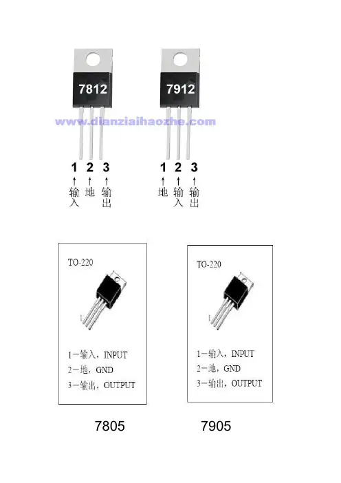
79XX系列集成压器是常用的固定负输出电压的三端集成稳压器,除输入电压和输出电压均为负值外,其他参数和特点与78XX系列集成稳压器相同。
79XX系列集成稳压的三个引脚为:1脚为接地端,2脚为输入端,3脚为输出端。
79XX系列集成稳压器的应用电路也很简单。
下图所示为输出-5V直流电压的稳压电源电路,IC采用集成稳压器7905,输出电流较大时应配上散热板。
LM7805中文资料目录1.lm7805介绍2.实际应用3.引脚序号、引脚功能4.lm7805应用电路5.7805电参数三端稳压集成电路lm7805。
电子产品中,常见的三端稳压集成电路有正电压输出的lm78 ××系列和负电压输出的lm79××系列。
顾名思义,三端IC 是指这种稳压用的集成电路,只有三条引脚输出,分别是输入端、接地端和输出端。
它的样子象是普通的三极管,TO- 220 的标准封装,也有lm9013样子的TO-92封装。
1.lm7805介绍用lm78/lm79系列三端稳压IC来组成稳压电源所需的外围元件极少,电路内部还有过流、过热及调整管的保护电路,使用起来可靠、方便,而且价格便宜。
该系列集成稳压IC型号中的lm78或lm79后面的数字代表该三端集成稳压电路的输出电压,如lm7806表示输出电压为正6V,lm7909表示输出电压为负9V。
因为三端固定集成稳压电路的使用方便,电子制作中经常采用。
最大输出电流1.5A,LM78XX系列输出电压分别为5V;6V;8V;9V;10V;12V;15V;18V;24V。
2.实际应用在实际应用中,应在三端集成稳压电路上安装足够大的散热器(当然小功率7805IC内部电路图.的条件下不用)。
当稳压管温度过高时,稳压性能将变差,甚至损坏。
当制作中需要一个能输出1.5A以上电流的稳压电源,通常采用几块三端稳压电路并联起来,使其最大输出电流为N个1.5A,但应用时需注意:并联使用的集成稳压电路应采用同一厂家、同一批号的产品,以保证参数的一致。
另外在输出电流上留有一定的余量,以避免个别集成稳压电路失效时导致其他电路的连锁烧毁。
在lm78 ** 、lm79 ** 系列三端稳压器中最常应用的是TO-220 和TO-202 两种封装。
这两种封装的图形以及引脚序号、引脚功能如附图所示。
图中的引脚号标注方法是按照引脚电位从高到底的顺序标注的。
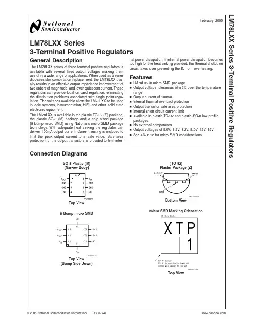
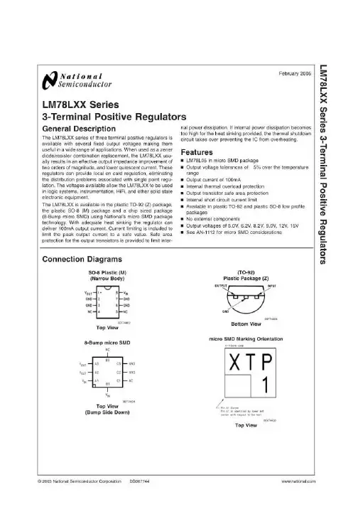
LM78LXX Series3-Terminal Positive RegulatorsGeneral DescriptionThe LM78LXX series of three terminal positive regulators isavailable with several fixed output voltages making themuseful in a wide range of applications.When used as a zenerdiode/resistor combination replacement,the LM78LXX usu-ally results in an effective output impedance improvement oftwo orders of magnitude,and lower quiescent current.Theseregulators can provide local on card regulation,eliminatingthe distribution problems associated with single point regu-lation.The voltages available allow the LM78LXX to be usedin logic systems,instrumentation,HiFi,and other solid stateelectronic equipment.The LM78LXX is available in the plastic TO-92(Z)package,the plastic SO-8(M)package and a chip sized package(8-Bump micro SMD)using National’s micro SMD packagetechnology.With adequate heat sinking the regulator candeliver100mA output current.Current limiting is included tolimit the peak output current to a safe value.Safe areaprotection for the output transistors is provided to limit inter-nal power dissipation.If internal power dissipation becomestoo high for the heat sinking provided,the thermal shutdowncircuit takes over preventing the IC from overheating.Featuresn LM78L05in micro SMD packagen Output voltage tolerances of±5%over the temperaturerangen Output current of100mAn Internal thermal overload protectionn Output transistor safe area protectionn Internal short circuit current limitn Available in plastic TO-92and plastic SO-8low profilepackagesn No external componentsn Output voltages of5.0V,6.2V,8.2V,9.0V,12V,15Vn See AN-1112for micro SMD considerations Connection DiagramsSO-8Plastic(M)(Narrow Body)00774402Top View8-Bump micro SMD00774424Top View(Bump Side Down)(TO-92)Plastic Package(Z)00774403Bottom Viewmicro SMD Marking Orientation00774433Top ViewFebruary2005LM78LXXSeries3-TerminalPositiveRegulators ©2005National Semiconductor Corporation Ordering InformationPackageOrder Number Output VoltageNSC Drawing Supplied As microSMDLM78L05IBP5V BPA08AAB Reel of 250LM78L05IBPX 5V BPA08AAB Reel of 3000LM78L09ITP 9V TPA08AAA Reel of 250LM78L09ITPX9V TPA08AAA Reel of 3000SOIC NarrowLM78L05ACM 5V M08A Rail of 95LM78L05ACMX 5V M08A Reel of 2500LM78L12ACM 12V M08A Rail of 95LM78L12ACMX 12V M08A Reel of 2500LM78L15ACM 15V M08A Rail of 95LM78L15ACMX15V M08A Reel of 2500TO-92LM78L05ACZ 5V Z03A Box of 1800LM78L62ACZ 6.2V Z03A Box of 1800LM78L82ACZ 8.2V Z03A Box of 1800LM78L09ACZ 9V Z03A Box of 1800LM78L12ACZ 12V Z03A Box of 1800LM78L15ACZ15VZ03ABox of 1800L M 78L X X S e r i e s 2Absolute Maximum Ratings (Note 1)If Military/Aerospace specified devices are required,please contact the National Semiconductor Sales Office/Distributors for availability and specifications.Power Dissipation (Note 5)Internally LimitedInput Voltage 35VStorage Temperature −65˚C to +150˚CESD Susceptibility (Note 2)1kVOperating Junction Temperature SO-8,TO-920˚C to 125˚C micro SMD −40˚C to 85˚CSoldering InformationInfrared or Convection (20sec.)235˚CWave Soldering (10sec.)260˚C (lead time)LM78LXX Electrical CharacteristicsLimits in standard typeface are for T J =25˚C,Bold typefaceapplies over 0˚C to 125˚C for SO-8and TO-92packages,and −40˚C to 85˚C for micro SMD package.Limits are guaran-teed by production testing or correlation techniques using standard Statistical Quality Control (SQC)methods.Unless other-wise specified:I O =40mA,C I =0.33µF,C O =0.1µF.LM78L05Unless otherwise specified,V IN =10V Symbol ParameterConditionsMin Typ Max UnitsV OOutput Voltage4.855.2V7V ≤V IN ≤20V 1mA ≤I O ≤40mA (Note 3)4.755.251mA ≤I O ≤70mA (Note 3)4.755.25∆V O Line Regulation 7V ≤V IN ≤20V 1875mV8V ≤V IN ≤20V 1054∆V O Load Regulation 1mA ≤I O ≤100mA 20601mA ≤I O ≤40mA530I Q Quiescent Current 35mA ∆I Q Quiescent Current Change 8V ≤V IN ≤20V 1.01mA ≤I O ≤40mA 0.1V nOutput Noise Voltage f =10Hz to 100kHz (Note 4)40µV Ripple Rejectionf =120Hz8V ≤V IN ≤16V4762dB I PKPeak Output Current140mA Average Output Voltage TempcoI O =5mA−0.65mV/˚C V IN (Min)Minimum Value of Input VoltageRequired to Maintain Line Regulation 6.77V θJAThermal Resistance (8-Bump micro SMD)230.9˚C/W LM78L62ACUnless otherwise specified,V IN =12V Symbol ParameterConditionsMin Typ Max UnitsV OOutput Voltage5.956.26.45V8.5V ≤V IN ≤20V 1mA ≤I O ≤40mA (Note 3)5.96.51mA ≤I O ≤70mA (Note 3)5.96.5LM78LXX Series3LM78LXX Electrical Characteristics Limits in standard typeface are for T J =25˚C,Bold typefaceapplies over 0˚C to 125˚C for SO-8and TO-92packages,and −40˚C to 85˚C for micro SMD package.Limits areguaranteed by production testing or correlation techniques using standard Statistical Quality Control (SQC)methods.Unless otherwise specified:I O =40mA,C I =0.33µF,C O =0.1µF.(Continued)LM78L62AC(Continued)Unless otherwise specified,V IN =12VSymbol ParameterConditions MinTyp Max Units∆V O Line Regulation 8.5V ≤V IN ≤20V 65175mV 9V ≤V IN ≤20V 55125∆V O Load Regulation 1mA ≤I O ≤100mA 13801mA ≤I O ≤40mA640I Q Quiescent Current 25.5mA ∆I Q Quiescent Current Change 8V ≤V IN ≤20V 1.51mA ≤I O ≤40mA 0.1V nOutput Noise Voltage f =10Hz to 100kHz (Note 4)50µV Ripple Rejectionf =120Hz10V ≤V IN ≤20V4046dB I PKPeak Output Current140mA Average Output Voltage TempcoI O =5mA−0.75mV/˚C V IN (Min)Minimum Value of Input VoltageRequired to Maintain Line Regulation7.9V LM78L82ACUnless otherwise specified,V IN =14V Symbol ParameterConditionsMin Typ Max UnitsV OOutput Voltage7.878.28.53V11V ≤V IN ≤23V 1mA ≤I O ≤40mA (Note 3)7.88.61mA ≤I O ≤70mA (Note 3)7.88.6∆V O Line Regulation 11V ≤V IN ≤23V 80175mV12V ≤V IN ≤23V 70125∆V O Load Regulation 1mA ≤I O ≤100mA 15801mA ≤I O ≤40mA840I Q Quiescent Current 25.5mA ∆I Q Quiescent Current Change 12V ≤V IN ≤23V 1.51mA ≤I O ≤40mA 0.1V nOutput Noise Voltage f =10Hz to 100kHz (Note 4)60µV Ripple Rejectionf =120Hz12V ≤V IN ≤22V3945dB I PKPeak Output Current140mA Average Output Voltage TempcoI O =5mA−0.8mV/˚C V IN (Min)Minimum Value of Input VoltageRequired to Maintain Line Regulation9.9V L M 78L X X S e r i e s 4LM78LXX Electrical Characteristics Limits in standard typeface are for T J =25˚C,Bold typefaceapplies over 0˚C to 125˚C for SO-8and TO-92packages,and −40˚C to 85˚C for micro SMD package.Limits areguaranteed by production testing or correlation techniques using standard Statistical Quality Control (SQC)methods.Unless otherwise specified:I O =40mA,C I =0.33µF,C O =0.1µF.(Continued)LM78L09ACUnless otherwise specified,V IN =15V Symbol ParameterConditionsMin Typ Max UnitsV OOutput Voltage8.649.09.36V11.5V ≤V IN ≤24V 1mA ≤I O ≤40mA (Note 3)8.559.451mA ≤I O ≤70mA (Note 3)8.559.45∆V O Line Regulation 11.5V ≤V IN ≤24V 100200mV13V ≤V IN ≤24V 90150∆V O Load Regulation 1mA ≤I O ≤100mA 20901mA ≤I O ≤40mA1045I Q Quiescent Current 25.5mA ∆I Q Quiescent Current Change 11.5V ≤V IN ≤24V 1.51mA ≤I O ≤40mA0.1V nOutput Noise Voltage 70µV Ripple Rejectionf =120Hz15V ≤V IN ≤25V3844dB I PKPeak Output Current140mA Average Output Voltage TempcoI O =5mA−0.9mV/˚C V IN (Min)Minimum Value of Input VoltageRequired to Maintain Line Regulation10.7V LM78L12ACUnless otherwise specified,V IN =19V Symbol ParameterConditionsMin Typ Max UnitsV OOutput Voltage11.51212.5V14.5V ≤V IN ≤27V 1mA ≤I O ≤40mA (Note 3)11.412.61mA ≤I O ≤70mA (Note 3)11.412.6∆V O Line Regulation 14.5V ≤V IN ≤27V 30180mV16V ≤V IN ≤27V 20110∆V O Load Regulation 1mA ≤I O ≤100mA 301001mA ≤I O ≤40mA1050I Q Quiescent Current 35mA ∆I Q Quiescent Current Change 16V ≤V IN ≤27V 11mA ≤I O ≤40mA0.1V nOutput Noise Voltage 80µV Ripple Rejectionf =120Hz15V ≤V IN ≤254054dB I PKPeak Output Current140mA Average Output Voltage TempcoI O =5mA−1.0mV/˚C LM78LXX Series5LM78LXX Electrical Characteristics Limits in standard typeface are for T J =25˚C,Bold typefaceapplies over 0˚C to 125˚C for SO-8and TO-92packages,and −40˚C to 85˚C for micro SMD package.Limits areguaranteed by production testing or correlation techniques using standard Statistical Quality Control (SQC)methods.Unless otherwise specified:I O =40mA,C I =0.33µF,C O =0.1µF.(Continued)LM78L12AC(Continued)Unless otherwise specified,V IN =19VSymbol ParameterConditionsMinTyp Max Units V IN (Min)Minimum Value of Input VoltageRequired to Maintain Line Regulation13.714.5VLM78L15ACUnless otherwise specified,V IN =23V Symbol ParameterConditionsMin Typ Max UnitsV OOutput Voltage14.415.015.6V17.5V ≤V IN ≤30V 1mA ≤I O ≤40mA (Note 3)14.2515.751mA ≤I O ≤70mA (Note 3)14.2515.75∆V O Line Regulation 17.5V ≤V IN ≤30V 37250mV20V ≤V IN ≤30V 25140∆V O Load Regulation 1mA ≤I O ≤100mA 351501mA ≤I O ≤40mA1275I QQuiescent Current 35mA ∆I QQuiescent Current Change 20V ≤V IN ≤30V 11mA ≤I O ≤40mA0.1V nOutput Noise Voltage 90µV Ripple Rejectionf =120Hz18.5V ≤V IN ≤28.5V3751dB I PKPeak Output Current140mA Average Output Voltage TempcoI O =5mA−1.3mV/˚C V IN (Min)Minimum Value of Input VoltageRequired to Maintain Line Regulation16.717.5V Note 1:Absolute Maximum Ratings indicate limits beyond which damage to the device may occur.Electrical specifications do not apply when operating the device outside of its stated operating conditions.Note 2:Human body model,1.5k Ωin series with 100pF.Note 3:Power dissipation ≤0.75W.Note 4:Recommended minimum load capacitance of 0.01µF to limit high frequency noise.Note 5:Typical thermal resistance values for the packages are:Z Package:θJC =60˚C/W,=θJA =230˚C/W M Package:θJA =180˚C/Wmicro SMD Package:θJA =230.9˚C/WL M 78L X X S e r i e s 6Typical Performance CharacteristicsMaximum Average Power Dissipation (Z Package)Peak Output Current0077441400774416Dropout Voltage Ripple Rejection0077441700774418Output Impedance Quiescent Current0077441900774420LM78LXX Series7Typical Performance Characteristics(Continued)Quiescent Current00774421Equivalent CircuitLM78LXX00774407L M 78L X X S e r i e s 8Typical ApplicationsFixed Output Regulator00774408*Required if the regulator is located more than 3"from the power supply filter.**See (Note 4)in the electrical characteristics table.Adjustable Output Regulator00774409V OUT =5V +(5V/R1+I Q )R25V/R1>3I Q ,load regulation (L r )≈[(R1+R2)/R1](L r of LM78L05)Current Regulator00774410I OUT =(V OUT /R1)+I Q>I Q =1.5mA over line and load changes5V,500mA Regulator with Short Circuit Protection00774411*Solid tantalum.**Heat sink Q1.***Optional:Improves ripple rejection and transient response.Load Regulation:0.6%0≤I L ≤250mA pulsed with t ON =50ms.LM78LXX Series9Typical Applications(Continued)±15V,100mA Dual Power Supply00774412*Solid tantalum.Variable Output Regulator 0.5V-18V00774413*Solid tantalum.V OUT =V G +5V,R1=(−V IN /I Q LM78L05)V OUT =5V (R2/R4)for (R2+R3)=(R4+R5)A 0.5V output will correspond to (R2/R4)=0.1(R3/R4)=0.9L M 78L X X S e r i e s 10Physical Dimensions inches(millimeters)unless otherwise notedNOTES:UNLESS OTHERWISE SPECIFIED1.EPOXY COATING2.63Sn/37Pb EUTECTIC BUMP3.RECOMMEND NON-SOLDER MASK DEFINED LANDING PAD.4.PIN A1IS ESTABLISHED BY LOWER LEFT CORNER WITH RESPECT TO TEXT ORIENTATION.REMAINING PINS ARE NUMBERED COUNTERCLOCKWISE.5.XXX IN DRAWING NUMBER REPRESENTS PACKAGE SIZE VARIATION WHERE X1IS PACKAGE WIDTH,X2IS PACKAGE LENGTH AND X3IS PACKAGE HEIGHT.6.REFERENCE JEDEC REGISTRATION MO-211,VARIATION BC.8-Bump micro SMD for LM78L05IBP OnlyNS Package Number BPA08AABX1=1.285mm X2=1.285mm X3=0.850mm LM78LXX Series 11Physical Dimensionsinches (millimeters)unless otherwise noted (Continued)8-Bump micro SMD for LM78L09ITP OnlyNS Package Number TPA08AAAX1=1.285mm X2=1.285mm X3=0.500mmL M 78L X X S e r i e s 12Physical Dimensions inches(millimeters)unless otherwise noted(Continued)S.O.Package(M)NS Package Number M08ALM78LXXSeries 13Physical Dimensionsinches (millimeters)unless otherwise noted (Continued)Molded Offset TO-92(Z)NS Package Number Z03ANational does not assume any responsibility for use of any circuitry described,no circuit patent licenses are implied and National reserves the right at any time without notice to change said circuitry and specifications.For the most current product information visit us at .LIFE SUPPORT POLICYNATIONAL’S PRODUCTS ARE NOT AUTHORIZED FOR USE AS CRITICAL COMPONENTS IN LIFE SUPPORT DEVICES OR SYSTEMS WITHOUT THE EXPRESS WRITTEN APPROVAL OF THE PRESIDENT AND GENERAL COUNSEL OF NATIONAL SEMICONDUCTOR CORPORATION.As used herein:1.Life support devices or systems are devices or systems which,(a)are intended for surgical implant into the body,or (b)support or sustain life,and whose failure to perform when properly used in accordance with instructions for use provided in the labeling,can be reasonably expected to result in a significant injury to the user.2.A critical component is any component of a life support device or system whose failure to perform can be reasonably expected to cause the failure of the life support device or system,or to affect its safety or effectiveness.BANNED SUBSTANCE COMPLIANCENational Semiconductor manufactures products and uses packing materials that meet the provisions of the Customer Products Stewardship Specification (CSP-9-111C2)and the Banned Substances and Materials of Interest Specification (CSP-9-111S2)and contain no ‘‘Banned Substances’’as defined in CSP-9-111S2.National Semiconductor Americas Customer Support CenterEmail:new.feedback@ Tel:1-800-272-9959National SemiconductorEurope Customer Support CenterFax:+49(0)180-5308586Email:europe.support@Deutsch Tel:+49(0)6995086208English Tel:+44(0)8702402171Français Tel:+33(0)141918790National Semiconductor Asia Pacific Customer Support CenterEmail:ap.support@National SemiconductorJapan Customer Support Center Fax:81-3-5639-7507Email:jpn.feedback@ Tel:81-3-5639-7560L M 78L X X S e r i e s 3-T e r m i n a l P o s i t i v e R e g u l a t o r s。
∙如何正确理解三端稳压器数据手册中各个参数的含义∙发布时间:2010-8-9 10:22:07 | 来源: 第一价值网| 查看: 1554次| 收藏 | 打印TAG:三端稳压器7805、7809、7812数据参数|输出电压|线性调整率|负载调整率|静态电流|静态电流变化量|输出噪声电压78系列三端稳压器是最常见的电子元件,很多初学者最先接触到的就是这类器件,但是,能够系统全面的介绍三端稳压器知识的书籍甚少,很多朋友都是一知半解,本想系统总结一下线性稳压器的各种参数及其意义,想了好久,还是没有头绪,就先从7805的数据手册上写的一些参数入手,来讨论一下各参数的意义吧。
LM7805是国家半导体开发出来比较成熟,较早的一种线性稳压半导体器件,现在仍然还有很多公司在使用,个人也用得比较多,因为很便宜且性能比较稳定。
常提到的三端稳压块7805就是指它了。
拿它作为例子很有代表性。
参数一:输出电压最简单的一个参数,就是稳压器的输出电压,能稳定在多少V,7805输出电压稳定在5V参数二:线性调整率稳压器的输入电压一般都比较宽,在该范围内,输入如果变化输出电压的变化有多大呢?该参数就是描述这种变化的一个参数。
很显然输出电压的变化是越小越好了,一般都是几毫伏。
拿7805作为例子来说吧,参考Data Sheet就可以知道,在常温,输出500mA电流的情况下,输入电压在7~25V之间变化的时候,输出电压的变化典型值为3mV,最大值为50mV参数三:负载调整率负载发生变化时,输出电压也会相应的发生变化,一般是负载越重,输出电压会有所下降,负载越轻输出电压会有所上升。
负载调整率就是反应这种变化的一个量。
看7805的Data Sheet可知,在负载变化在5mA~1.5A时,输出电压的变化范围在10~50mV参数四:静态电流对于线性稳压器来说是一个非常重要的参数。
该电流为驱动大功率调整管所必须的,它不流向负载,而是直接流向地,因此该电流是越小越好。

LM78LXX Series3-Terminal Positive RegulatorsGeneral DescriptionThe LM78LXX series of three terminal positive regulators isavailable with several fixed output voltages making themuseful in a wide range of applications.When used as a zenerdiode/resistor combination replacement,the LM78LXX usu-ally results in an effective output impedance improvement oftwo orders of magnitude,and lower quiescent current.Theseregulators can provide local on card regulation,eliminatingthe distribution problems associated with single point regu-lation.The voltages available allow the LM78LXX to be usedin logic systems,instrumentation,HiFi,and other solid stateelectronic equipment.The LM78LXX is available in the plastic TO-92(Z)package,the plastic SO-8(M)package and a chip sized package(8-Bump micro SMD)using National’s micro SMD packagetechnology.With adequate heat sinking the regulator candeliver100mA output current.Current limiting is included tolimit the peak output current to a safe value.Safe areaprotection for the output transistors is provided to limit inter-nal power dissipation.If internal power dissipation becomestoo high for the heat sinking provided,the thermal shutdowncircuit takes over preventing the IC from overheating.Featuresn LM78L05in micro SMD packagen Output voltage tolerances of±5%over the temperaturerangen Output current of100mAn Internal thermal overload protectionn Output transistor safe area protectionn Internal short circuit current limitn Available in plastic TO-92and plastic SO-8low profilepackagesn No external componentsn Output voltages of5.0V,6.2V,8.2V,9.0V,12V,15Vn See AN-1112for micro SMD considerations Connection DiagramsSO-8Plastic(M)(Narrow Body)00774402Top View8-Bump micro SMD00774424Top View(Bump Side Down)(TO-92)Plastic Package(Z)00774403Bottom Viewmicro SMD Marking Orientation00774433Top ViewFebruary2005LM78LXXSeries3-TerminalPositiveRegulators ©2005National Semiconductor Corporation Ordering InformationPackageOrder Number Output VoltageNSC Drawing Supplied As microSMDLM78L05IBP5V BPA08AAB Reel of 250LM78L05IBPX 5V BPA08AAB Reel of 3000LM78L09ITP 9V TPA08AAA Reel of 250LM78L09ITPX9V TPA08AAA Reel of 3000SOIC NarrowLM78L05ACM 5V M08A Rail of 95LM78L05ACMX 5V M08A Reel of 2500LM78L12ACM 12V M08A Rail of 95LM78L12ACMX 12V M08A Reel of 2500LM78L15ACM 15V M08A Rail of 95LM78L15ACMX15V M08A Reel of 2500TO-92LM78L05ACZ 5V Z03A Box of 1800LM78L62ACZ 6.2V Z03A Box of 1800LM78L82ACZ 8.2V Z03A Box of 1800LM78L09ACZ 9V Z03A Box of 1800LM78L12ACZ 12V Z03A Box of 1800LM78L15ACZ15VZ03ABox of 1800L M 78L X X S e r i e s 2Absolute Maximum Ratings (Note 1)If Military/Aerospace specified devices are required,please contact the National Semiconductor Sales Office/Distributors for availability and specifications.Power Dissipation (Note 5)Internally LimitedInput Voltage 35VStorage Temperature −65˚C to +150˚CESD Susceptibility (Note 2)1kVOperating Junction Temperature SO-8,TO-920˚C to 125˚C micro SMD −40˚C to 85˚CSoldering InformationInfrared or Convection (20sec.)235˚CWave Soldering (10sec.)260˚C (lead time)LM78LXX Electrical CharacteristicsLimits in standard typeface are for T J =25˚C,Bold typefaceapplies over 0˚C to 125˚C for SO-8and TO-92packages,and −40˚C to 85˚C for micro SMD package.Limits are guaran-teed by production testing or correlation techniques using standard Statistical Quality Control (SQC)methods.Unless other-wise specified:I O =40mA,C I =0.33µF,C O =0.1µF.LM78L05Unless otherwise specified,V IN =10V Symbol ParameterConditionsMin Typ Max UnitsV OOutput Voltage4.855.2V7V ≤V IN ≤20V 1mA ≤I O ≤40mA (Note 3)4.755.251mA ≤I O ≤70mA (Note 3)4.755.25∆V O Line Regulation 7V ≤V IN ≤20V 1875mV8V ≤V IN ≤20V 1054∆V O Load Regulation 1mA ≤I O ≤100mA 20601mA ≤I O ≤40mA530I Q Quiescent Current 35mA ∆I Q Quiescent Current Change 8V ≤V IN ≤20V 1.01mA ≤I O ≤40mA 0.1V nOutput Noise Voltage f =10Hz to 100kHz (Note 4)40µV Ripple Rejectionf =120Hz8V ≤V IN ≤16V4762dB I PKPeak Output Current140mA Average Output Voltage TempcoI O =5mA−0.65mV/˚C V IN (Min)Minimum Value of Input VoltageRequired to Maintain Line Regulation 6.77V θJAThermal Resistance (8-Bump micro SMD)230.9˚C/W LM78L62ACUnless otherwise specified,V IN =12V Symbol ParameterConditionsMin Typ Max UnitsV OOutput Voltage5.956.26.45V8.5V ≤V IN ≤20V 1mA ≤I O ≤40mA (Note 3)5.96.51mA ≤I O ≤70mA (Note 3)5.96.5LM78LXX Series3LM78LXX Electrical Characteristics Limits in standard typeface are for T J =25˚C,Bold typefaceapplies over 0˚C to 125˚C for SO-8and TO-92packages,and −40˚C to 85˚C for micro SMD package.Limits areguaranteed by production testing or correlation techniques using standard Statistical Quality Control (SQC)methods.Unless otherwise specified:I O =40mA,C I =0.33µF,C O =0.1µF.(Continued)LM78L62AC(Continued)Unless otherwise specified,V IN =12VSymbol ParameterConditions MinTyp Max Units∆V O Line Regulation 8.5V ≤V IN ≤20V 65175mV 9V ≤V IN ≤20V 55125∆V O Load Regulation 1mA ≤I O ≤100mA 13801mA ≤I O ≤40mA640I Q Quiescent Current 25.5mA ∆I Q Quiescent Current Change 8V ≤V IN ≤20V 1.51mA ≤I O ≤40mA 0.1V nOutput Noise Voltage f =10Hz to 100kHz (Note 4)50µV Ripple Rejectionf =120Hz10V ≤V IN ≤20V4046dB I PKPeak Output Current140mA Average Output Voltage TempcoI O =5mA−0.75mV/˚C V IN (Min)Minimum Value of Input VoltageRequired to Maintain Line Regulation7.9V LM78L82ACUnless otherwise specified,V IN =14V Symbol ParameterConditionsMin Typ Max UnitsV OOutput Voltage7.878.28.53V11V ≤V IN ≤23V 1mA ≤I O ≤40mA (Note 3)7.88.61mA ≤I O ≤70mA (Note 3)7.88.6∆V O Line Regulation 11V ≤V IN ≤23V 80175mV12V ≤V IN ≤23V 70125∆V O Load Regulation 1mA ≤I O ≤100mA 15801mA ≤I O ≤40mA840I Q Quiescent Current 25.5mA ∆I Q Quiescent Current Change 12V ≤V IN ≤23V 1.51mA ≤I O ≤40mA 0.1V nOutput Noise Voltage f =10Hz to 100kHz (Note 4)60µV Ripple Rejectionf =120Hz12V ≤V IN ≤22V3945dB I PKPeak Output Current140mA Average Output Voltage TempcoI O =5mA−0.8mV/˚C V IN (Min)Minimum Value of Input VoltageRequired to Maintain Line Regulation9.9V L M 78L X X S e r i e s 4LM78LXX Electrical Characteristics Limits in standard typeface are for T J =25˚C,Bold typefaceapplies over 0˚C to 125˚C for SO-8and TO-92packages,and −40˚C to 85˚C for micro SMD package.Limits areguaranteed by production testing or correlation techniques using standard Statistical Quality Control (SQC)methods.Unless otherwise specified:I O =40mA,C I =0.33µF,C O =0.1µF.(Continued)LM78L09ACUnless otherwise specified,V IN =15V Symbol ParameterConditionsMin Typ Max UnitsV OOutput Voltage8.649.09.36V11.5V ≤V IN ≤24V 1mA ≤I O ≤40mA (Note 3)8.559.451mA ≤I O ≤70mA (Note 3)8.559.45∆V O Line Regulation 11.5V ≤V IN ≤24V 100200mV13V ≤V IN ≤24V 90150∆V O Load Regulation 1mA ≤I O ≤100mA 20901mA ≤I O ≤40mA1045I Q Quiescent Current 25.5mA ∆I Q Quiescent Current Change 11.5V ≤V IN ≤24V 1.51mA ≤I O ≤40mA0.1V nOutput Noise Voltage 70µV Ripple Rejectionf =120Hz15V ≤V IN ≤25V3844dB I PKPeak Output Current140mA Average Output Voltage TempcoI O =5mA−0.9mV/˚C V IN (Min)Minimum Value of Input VoltageRequired to Maintain Line Regulation10.7V LM78L12ACUnless otherwise specified,V IN =19V Symbol ParameterConditionsMin Typ Max UnitsV OOutput Voltage11.51212.5V14.5V ≤V IN ≤27V 1mA ≤I O ≤40mA (Note 3)11.412.61mA ≤I O ≤70mA (Note 3)11.412.6∆V O Line Regulation 14.5V ≤V IN ≤27V 30180mV16V ≤V IN ≤27V 20110∆V O Load Regulation 1mA ≤I O ≤100mA 301001mA ≤I O ≤40mA1050I Q Quiescent Current 35mA ∆I Q Quiescent Current Change 16V ≤V IN ≤27V 11mA ≤I O ≤40mA0.1V nOutput Noise Voltage 80µV Ripple Rejectionf =120Hz15V ≤V IN ≤254054dB I PKPeak Output Current140mA Average Output Voltage TempcoI O =5mA−1.0mV/˚C LM78LXX Series5LM78LXX Electrical Characteristics Limits in standard typeface are for T J =25˚C,Bold typefaceapplies over 0˚C to 125˚C for SO-8and TO-92packages,and −40˚C to 85˚C for micro SMD package.Limits areguaranteed by production testing or correlation techniques using standard Statistical Quality Control (SQC)methods.Unless otherwise specified:I O =40mA,C I =0.33µF,C O =0.1µF.(Continued)LM78L12AC(Continued)Unless otherwise specified,V IN =19VSymbol ParameterConditionsMinTyp Max Units V IN (Min)Minimum Value of Input VoltageRequired to Maintain Line Regulation13.714.5VLM78L15ACUnless otherwise specified,V IN =23V Symbol ParameterConditionsMin Typ Max UnitsV OOutput Voltage14.415.015.6V17.5V ≤V IN ≤30V 1mA ≤I O ≤40mA (Note 3)14.2515.751mA ≤I O ≤70mA (Note 3)14.2515.75∆V O Line Regulation 17.5V ≤V IN ≤30V 37250mV20V ≤V IN ≤30V 25140∆V O Load Regulation 1mA ≤I O ≤100mA 351501mA ≤I O ≤40mA1275I QQuiescent Current 35mA ∆I QQuiescent Current Change 20V ≤V IN ≤30V 11mA ≤I O ≤40mA0.1V nOutput Noise Voltage 90µV Ripple Rejectionf =120Hz18.5V ≤V IN ≤28.5V3751dB I PKPeak Output Current140mA Average Output Voltage TempcoI O =5mA−1.3mV/˚C V IN (Min)Minimum Value of Input VoltageRequired to Maintain Line Regulation16.717.5V Note 1:Absolute Maximum Ratings indicate limits beyond which damage to the device may occur.Electrical specifications do not apply when operating the device outside of its stated operating conditions.Note 2:Human body model,1.5k Ωin series with 100pF.Note 3:Power dissipation ≤0.75W.Note 4:Recommended minimum load capacitance of 0.01µF to limit high frequency noise.Note 5:Typical thermal resistance values for the packages are:Z Package:θJC =60˚C/W,=θJA =230˚C/W M Package:θJA =180˚C/Wmicro SMD Package:θJA =230.9˚C/WL M 78L X X S e r i e s 6Typical Performance CharacteristicsMaximum Average Power Dissipation (Z Package)Peak Output Current0077441400774416Dropout Voltage Ripple Rejection0077441700774418Output Impedance Quiescent Current0077441900774420LM78LXX Series7Typical Performance Characteristics(Continued)Quiescent Current00774421Equivalent CircuitLM78LXX00774407L M 78L X X S e r i e s 8Typical ApplicationsFixed Output Regulator00774408*Required if the regulator is located more than 3"from the power supply filter.**See (Note 4)in the electrical characteristics table.Adjustable Output Regulator00774409V OUT =5V +(5V/R1+I Q )R25V/R1>3I Q ,load regulation (L r )≈[(R1+R2)/R1](L r of LM78L05)Current Regulator00774410I OUT =(V OUT /R1)+I Q>I Q =1.5mA over line and load changes5V,500mA Regulator with Short Circuit Protection00774411*Solid tantalum.**Heat sink Q1.***Optional:Improves ripple rejection and transient response.Load Regulation:0.6%0≤I L ≤250mA pulsed with t ON =50ms.LM78LXX Series9Typical Applications(Continued)±15V,100mA Dual Power Supply00774412*Solid tantalum.Variable Output Regulator 0.5V-18V00774413*Solid tantalum.V OUT =V G +5V,R1=(−V IN /I Q LM78L05)V OUT =5V (R2/R4)for (R2+R3)=(R4+R5)A 0.5V output will correspond to (R2/R4)=0.1(R3/R4)=0.9L M 78L X X S e r i e s 10Physical Dimensions inches(millimeters)unless otherwise notedNOTES:UNLESS OTHERWISE SPECIFIED1.EPOXY COATING2.63Sn/37Pb EUTECTIC BUMP3.RECOMMEND NON-SOLDER MASK DEFINED LANDING PAD.4.PIN A1IS ESTABLISHED BY LOWER LEFT CORNER WITH RESPECT TO TEXT ORIENTATION.REMAINING PINS ARE NUMBERED COUNTERCLOCKWISE.5.XXX IN DRAWING NUMBER REPRESENTS PACKAGE SIZE VARIATION WHERE X1IS PACKAGE WIDTH,X2IS PACKAGE LENGTH AND X3IS PACKAGE HEIGHT.6.REFERENCE JEDEC REGISTRATION MO-211,VARIATION BC.8-Bump micro SMD for LM78L05IBP OnlyNS Package Number BPA08AABX1=1.285mm X2=1.285mm X3=0.850mm LM78LXX Series 11Physical Dimensionsinches (millimeters)unless otherwise noted (Continued)8-Bump micro SMD for LM78L09ITP OnlyNS Package Number TPA08AAAX1=1.285mm X2=1.285mm X3=0.500mmL M 78L X X S e r i e s 12Physical Dimensions inches(millimeters)unless otherwise noted(Continued)S.O.Package(M)NS Package Number M08ALM78LXXSeries 13Physical Dimensionsinches (millimeters)unless otherwise noted (Continued)Molded Offset TO-92(Z)NS Package Number Z03ANational does not assume any responsibility for use of any circuitry described,no circuit patent licenses are implied and National reserves the right at any time without notice to change said circuitry and specifications.For the most current product information visit us at .LIFE SUPPORT POLICYNATIONAL’S PRODUCTS ARE NOT AUTHORIZED FOR USE AS CRITICAL COMPONENTS IN LIFE SUPPORT DEVICES OR SYSTEMS WITHOUT THE EXPRESS WRITTEN APPROVAL OF THE PRESIDENT AND GENERAL COUNSEL OF NATIONAL SEMICONDUCTOR CORPORATION.As used herein:1.Life support devices or systems are devices or systems which,(a)are intended for surgical implant into the body,or (b)support or sustain life,and whose failure to perform when properly used in accordance with instructions for use provided in the labeling,can be reasonably expected to result in a significant injury to the user.2.A critical component is any component of a life support device or system whose failure to perform can be reasonably expected to cause the failure of the life support device or system,or to affect its safety or effectiveness.BANNED SUBSTANCE COMPLIANCENational Semiconductor manufactures products and uses packing materials that meet the provisions of the Customer Products Stewardship Specification (CSP-9-111C2)and the Banned Substances and Materials of Interest Specification (CSP-9-111S2)and contain no ‘‘Banned Substances’’as defined in CSP-9-111S2.National Semiconductor Americas Customer Support CenterEmail:new.feedback@ Tel:1-800-272-9959National SemiconductorEurope Customer Support CenterFax:+49(0)180-5308586Email:europe.support@Deutsch Tel:+49(0)6995086208English Tel:+44(0)8702402171Français Tel:+33(0)141918790National Semiconductor Asia Pacific Customer Support CenterEmail:ap.support@National SemiconductorJapan Customer Support Center Fax:81-3-5639-7507Email:jpn.feedback@ Tel:81-3-5639-7560L M 78L X X S e r i e s 3-T e r m i n a l P o s i t i v e R e g u l a t o r s。
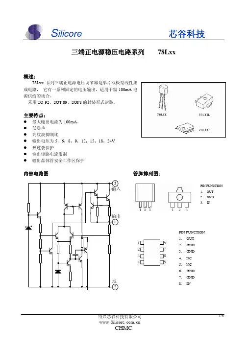
常用三端稳压功能介绍表型号(规格) 功能简介79L05 -5V稳压器(100ma)79L06 -6V稳压器(100ma)79L08 -8V稳压器(100ma)KA1L0380RB Power SwitchKA5L0380R Power SwitchKA78R05 Low Dropout V oltage Regulator(1A)PQ05RD11 ASO 保护功能低功耗稳压器(1A)[四端稳压]PQ05RD21 ASO 保护功能低功耗稳压器(2A)[四端稳压]LM1575T-3.3 3.3V简易开关电源稳压器(1A)LM1575T-5.0 5V简易开关电源稳压器(1A)LM1575T-12 12V简易开关电源稳压器(1A)LM1575T-15 15V简易开关电源稳压器(1A)LM1575T-ADJ 简易开关电源稳压器(1A可调1.23 to 37)LM1575HVT-3.3 3.3V简易开关电源稳压器(1A)LM1575HVT-5.0 5V简易开关电源稳压器(1A)LM1575HVT-12 12V简易开关电源稳压器(1A)LM1575HVT-15 15V简易开关电源稳压器(1A)LM1575HVT-ADJ 简易开关电源稳压器(1A可调1.23 to 37) LM2575T-3.3 3.3V简易开关电源稳压器(1A)LM2575T-5.0 5V简易开关电源稳压器(1A)LM2575T-12 12V简易开关电源稳压器(1A)LM2575T-15 15V简易开关电源稳压器(1A)LM2575T-ADJ 简易开关电源稳压器(1A可调1.23 to 37)LM2575HVT-3.3 3.3V简易开关电源稳压器(1A)LM2575HVT-5.0 5V简易开关电源稳压器(1A)LM2575HVT-12 12V简易开关电源稳压器(1A)LM2575HVT-15 15V简易开关电源稳压器(1A)LM2575HVT-ADJ 简易开关电源稳压器(1A可调1.23 to 37) LM2576T-3.3 3.3V简易开关电源稳压器(3A)LM2576T-5.0 5.0V简易开关电源稳压器(3A)LM2576T-12 12V简易开关电源稳压器(3A)LM2576T-15 15V简易开关电源稳压器(3A)LM2576T-ADJ 简易开关电源稳压器(3A可调1.23V to 37V) LM2576HVT-3.3 3.3V简易开关电源稳压器(3A)LM2576HVT-5.0 5.0V简易开关电源稳压器(3A)LM2576HVT-12 12V简易开关电源稳压器(3A)LM2576HVT-15 15V简易开关电源稳压器(3A)LM2576HVT-ADJ 简易开关电源稳压器(3A可调1.23V to 37V) LM2930T-5.0 5.0V低压差稳压器LM2930T-8.0 8.0V低压差稳压器LM2931AZ-5.0 5.0V低压差稳压器(TO-92)LM2931T-5.0 5.0V低压差稳压器LM2931CT 3V to 29V低压差稳压器(TO-2205PIN) LM2940CT-5.0 5.0V低压差稳压器LM2940CT-8.0 8.0V低压差稳压器LM2940CT-9.0 9.0V低压差稳压器LM2940CT-10 10V低压差稳压器LM2940CT-12 12V低压差稳压器LM2940CT-15 15V低压差稳压器LM123K(NS) 5V稳压器(3A)LM323K(NS) 5V稳压器(3A)LM117K(NS) 1.2V to 37V三端正可调稳压器(1.5A) LM317LZ(NS) 1.2V to 37V三端正可调稳压器(0.1A) LM317T(NS) 1.2V to 37V三端正可调稳压器(1.5A) LM317K(NS) 1.2V to 37V三端正可调稳压器(1.5A) LM133K(NS) 三端可调-1.2V to -37V稳压器(3.0A) LM333K(NS) 三端可调-1.2V to -37V稳压器(3.0A) LM337K(NS) 三端可调-1.2V to -37V稳压器(1.5A) LM337T(NS) 三端可调-1.2V to -37V稳压器(1.5A) LM337LZ(NS) 三端可调-1.2V to -37V稳压器(0.1A) LM150K(NS) 三端可调1.2V to 32V稳压器(3A)LM350K(NS) 三端可调1.2V to 32V稳压器(3A)LM350T(NS) 三端可调1.2V to 32V稳压器(3A)LM138K(NS) 三端正可调1.2V to 32V稳压器(5A) LM338T(NS) 三端正可调1.2V to 32V稳压器(5A) LM338K(NS) 三端正可调1.2V to 32V稳压器(5A) LM336Z-2.5(NS) 2.5V精密基准电压源LM336Z-5.0(NS) 5.0V精密基准电压源LM385Z-1.2(NS) 1.2V精密基准电压源LM385Z-2.5(NS) 2.5V精密基准电压源LM399H 6.9999V精密基准电压源LM431ACZ(NS) 精密可调2.5V to 36V基准稳压源LM723 高精度可调2V to 37V稳压器LM105 高精度可调4.5V to 40V稳压器LM305 高精度可调4.5V to 40V稳压器MC1403 2.5V基准电压源MC34063 充电控制器SG3524 脉宽调制开关电源控制器TL431(TI) 精密可调2.5V to 36V基准稳压源TL494 脉宽调制开关电源控制器TL497 频率调制开关电源控制器TL7705(TI) 电池供电/欠压控制器HT1015 1.5V V oltage RegulatorHT7130=HT1030 3.0V High V oltage RegulatorHT7133=HT1033 3.3V High V oltage RegulatorHT7136=HT1036 3.6V High V oltage RegulatorHT7144=HT1044 4.4V High V oltage Regulator HT7150=HT1050 5.0V High V oltage Regulator HT7022 2.2V V oltage DetectorHT7024 2.4V V oltage DetectorHT7027 2.7V V oltage DetectorHT7033 3.3V V oltage DetectorHT7039 3.9V V oltage DetectorHT7044 4.4V V oltage DetectorHT7050 5.0V V oltage DetectorHT7070 7.0V V oltage DetectorLM7805 5V稳压器(1A)LM7806 6V稳压器(1A)LM7808 8V稳压器(1A)LM7809 9V稳压议(1A)LM7812 12V稳压器(1A)LM7815 15V稳压器(1A)LM7818 18V稳压器(1A)LM7824 24V稳压器(1A)LM7905 -5V稳压器(1A)LM7906 -6V稳压器(1A)LM7908 -8V稳压器(1A)LM7909 -9V稳压器(1A)LM7912 -12V稳压器(1A)LM7915 -15V稳压器(1A)LM7918 -18V稳压器(1A)LM7924 -24V稳压器(1A)78L05 5V稳压器(100ma)78L06 6V稳压器(100ma)78L08 8V稳压器(100ma)78L09 9V稳压器(100ma)78L12 12V稳压器(100ma)78L15 15V稳压器(100ma)78L18 18V稳压器(100ma)78L24 24V稳压器(100ma)。
认识电路中的三端稳压器
在电路板上,我们经常会看到一个类似三极管的元件---三端稳压器。
三端稳压器常用在需要电压变换的地方。
如18伏变12伏、12伏变5伏。
常见的三端稳压器有78系列的7805、7808、7809、7812、7824等。
78后面的数字代表稳压器输出的电压值。
78系列的稳压器输出都为正压。
如7805代表输出正5伏、7812代表输出正12伏。
另一种输出负压的三端稳压器是79系列的。
如7905代表输出伏5伏电压、7912代表输出负12伏电压。
有的三端稳压器标注带字母,那是代表承受电流。
如输出电流以78(或79)后面加字母来区分。
L表示0.1;AM表示0.5A,无字母表示1.5A,如78L05表求5V 0.1A。
常见的三端稳压器管脚排列一般是带字的那面朝向我们时,左边的第一个脚为输入正极,中间为负极,最右边为输出正极。
在三端稳压器输入端与输出端都会有一个电解电容。
使用三端稳压器要注意输入与输出之间的电压差不能过小。
以7805为例,该三端稳压器的固定输出电压是5V,而输入电压至少大于7V,这样输入/输出之间有2-3V及以上的压差。
使调整管保证工作在放大区。
但压差取得大时,又会增加集成块的功耗,所以,两者应兼顾,即既保证在最大负载电流时调整管不进入饱和,又不至于功耗偏大。
另外一般在三端稳压器的输入输出端接一个二极管,用来防止输入端短路时,输出端存储的电荷通过稳压器,而损坏器件。
三端稳压器的故障率不高,最常见的是管脚开焊。
但在维修中常常是我们检测电压是否正常的一个检测点,所以很有必要对它进行了解。
1A Positive Voltage RegulatorFeatures Applications• Output Current up to 1A• Fixed output voltage of 5V, 6V, 8V, 9V,10V, 12V,15V, 18V and 24V available • Thermal overload shutdown protection • Short circuit current limiting• Output transistor SOA protection • RoHS Compliance• High Efficiency Linear Regulator• Post Regulation for Switching Supply • Microprocessor Power Supply • Mother BoardTO-220Block DiagramAbsolute Maximum RatingsSymbolDescriptionRatingsUnitV OUT = 3.3~18V 35V IN Input VoltageV OUT =20~24V 40V I OUT Output Current 1 A P D Power DissipationTO-220Internally LimitedmWT J Junction Temperature 150 T OPR Operating Temperature Range -20 ~ 150 ° C T STG Storage Temperature Range -55 ~ 150 ° CNote: 1. Absolute maximum ratings are stress ratings only and functional device operation is not implied. The device could be damaged beyond Absolute maximum ratings.2. The maximum steady state usable output current are dependent on input voltage, heat sinking, lead length of the package and copper pattern of PCB. The data are showed as electricalcharacteristics table represents pulse test conditions with junction temperatures specified atthe initiation of test.Electrical Characteristics (T J =25° C, P D ≦15W, unless otherwise specified)For SL7805 (V IN =10V, I OUT =0.5A, C1=0.33µF, C O =0.1µF)SL7805Symbol DescriptionMin.Typ.Max.Unit Test Conditions4.805.0 5.20 V I OUT =5mA-1.0AV OUT Output Voltage 4.75 - 5.25 V 7.5V ≤V IN ≤20V, I OUT =5mA-1.0A - - 50 mV I OUT =5mA-1.0A ∆V OUT Load Regulation - - 25 mV I OUT =0.25A-0.75A - - 50 mV 7V ≤V IN ≤25V ∆V OUT Line Regulation - - 50 mV 7.5V ≤V IN ≤20V, I OUT =1.0A I Q Quiescent Current - - 8.0 mA I OUT ≦1.0A - - 1.0 mA 7.5V ≤V IN ≤20V ∆I Q Quiescent Current Change - - 0.5 mA I OUT =5mA-1.0A eN Output Noise Voltage - 40 - µV 10Hz ≤f ≤100KHz ∆V O /∆T Temperature coefficient of V OUT- -0.6 - mV/℃I OUT =5mARR Ripple Rejection 62 80 - dB8V ≤V IN ≤18V, f=120HzI PEAK Peak Output Current - 1.8 - A - I SC Short-Circuit Current - 250 - mA V IN =35VV DDropout Voltage- 2.0 - V-For SL7806 (V IN =11V, I OUT =0.5A, C1=0.33µF, C O =0.1µF)SL7806Symbol DescriptionMin.Typ.Max.Unit Test Conditions5.766.0 6.24 V I OUT =5mA-1.0AV OUT Output Voltage 5.70 - 6.30 V 8.5V ≤V IN ≤21V, I OUT =5mA-1.0A - - 60 mV I OUT =5mA-1.0A ∆V OUT Load Regulation - - 30 mV I OUT =0.25A-0.75A - - 60 mV 8V ≤V IN ≤25V ∆V OUT Line Regulation - - 60 mV 8.5V ≤V IN ≤21V, I OUT =1.0A I Q Quiescent Current - - 8.0 mA I OUT ≦1.0A - - 1.0 mA 8.5V ≤V IN ≤21V ∆I Q Quiescent Current Change - - 0.5 mA I OUT =5mA-1.0A eN Output Noise Voltage- 45 - µV 10Hz ≤f ≤100KHz ∆V O /∆T Temperature coefficient of V OUT- -0.7 - mV/℃I OUT =5mARRRipple Rejection 59 75 - dB9V ≤V IN ≤19V, f=120HzI PEAK Peak Output Current - 1.8 - A - I SC Short-Circuit Current - 250 - mA V IN =35VV D Dropout Voltage- 2.0 - V-For SL7808 (V IN =14V, I OUT =0.5A, C1=0.33µF, C O =0.1µF)SL7808Symbol DescriptionMin.Typ.Max.Unit Test Conditions7.68 8.0 8.32 V I OUT =5mA-1.0AV OUT Output Voltage 7.60 - 8.40 V 10.5V ≤V IN ≤23V, I OUT =5mA-1.0A - - 80 mV I OUT =5mA-1.0A ∆V OUT Load Regulation - - 40 mV I OUT =0.25A-0.75A - - 80 mV 10.5V ≤V IN ≤25V ∆V OUT Line Regulation - - 80 mV 10.5V ≤V IN ≤23V, I OUT =1.0A I Q Quiescent Current - - 8.0 mA I OUT ≦1.0A - - 1.0 mA 10.5V ≤V IN ≤23V ∆I Q Quiescent Current Change - - 0.5 mA I OUT =5mA-1.0A eN Output Noise Voltage - 58 - µV 10Hz ≤f ≤100KHz ∆V O /∆T Temperature coefficient of V OUT- -0.9 - mV/℃I OUT =5mARR Ripple Rejection 56 72 - dB 11.5V ≤V IN ≤21.5V, f=120Hz I PEAK Peak Output Current - 1.8 - A - I SC Short-Circuit Current - 250 - mA V IN =35V V DDropout Voltage- 2.0 - V -For SL7809 (V IN =15V, I OUT =0.5A, C1=0.33µF, C O =0.1µF)SL7809Symbol DescriptionMin.Typ.Max.Unit Test Conditions8.64 9.0 9.36 V I OUT =5mA-1.0AV OUT Output Voltage 8.55 - 9.45 V 11.5V ≤V IN ≤24V, I OUT =5mA-1.0A - - 90 mV I OUT =5mA-1.0A ∆V OUT Load Regulation - - 45 mV I OUT =0.25A-0.75A - - 90 mV 11.5V ≤V IN ≤25V ∆V OUT Line Regulation - - 90 mV 11.5V ≤V IN ≤24V, I OUT =1.0A I Q Quiescent Current - - 8.0 mA I OUT ≦1.0A - - 1.0 mA 11.5V ≤V IN ≤24V ∆I Q Quiescent Current Change - - 0.5 mA I OUT =5mA-1.0A eN Output Noise Voltage- 58 - µV 10Hz ≤f ≤100KHz ∆V O /∆T Temperature coefficient of V OUT- -1.1 - mV/℃I OUT =5mARRRipple Rejection 56 72 - dB 12.5V ≤V IN ≤22.5V, f=120HzI PEAKPeak Output Current - 1.8 - A - I SC Short-Circuit Current - 250 - mA V IN =35V V D Dropout Voltage- 2.0 - V -For SL7810 (V IN =16V, I OUT =0.5A, C1=0.33µF, C O =0.1µF)SL7810Symbol DescriptionMin.Typ.Max.Unit Test Conditions9.60 10.0 10.40 V I OUT =5mA-1.0A V OUT Output Voltage 9.50 - 10.50 V 12.5V ≤V IN ≤25V, I OUT =5mA-1.0A - - 100 mV I OUT =5mA-1.0A ∆V OUT Load Regulation - - 50 mV I OUT =0.25A-0.75A - - 100 mV 13V ≤V IN ≤25V ∆V OUT Line Regulation - - 100 mV 13V ≤V IN ≤25V, I OUT =1.0A I Q Quiescent Current - - 8.0 mA I OUT ≦1.0A - - 1.0 mA 12.6V ≤V IN ≤25V ∆I Q Quiescent Current Change - - 0.5 mA I OUT =5mA-1.0A eN Output Noise Voltage - 58 - µV 10Hz ≤f ≤100KHz ∆V O /∆T Temperature coefficient of V OUT- -1.1 - mV/℃I OUT =5mARR Ripple Rejection 56 72 - dB13V ≤V IN ≤23V, f=120HzI PEAKPeak Output Current - 1.8 - A - I SC Short-Circuit Current - 250 - mA V IN =35VV DDropout Voltage- 2.0 - V-For SL7812 (V IN =19V, I OUT =0.5A, C1=0.33µF, C O =0.1µF)SL7812Symbol DescriptionMin.Typ.Max.Unit Test Conditions11.52 12.0 12.48 V I OUT =5mA-1.0AV OUT Output Voltage 11.40 - 12.60 V 14.5V ≤V IN ≤27V, I OUT =5mA-1.0A - - 120 mV I OUT =5mA-1.0A ∆V OUT Load Regulation - - 60 mV I OUT =0.25A-0.75A - - 120 mV 14.5V ≤V IN ≤30V ∆V OUT Line Regulation - - 120 mV 14.6V ≤V IN ≤27V, I OUT =1.0A I Q Quiescent Current - - 8.0 mA I OUT ≦1.0A - - 1.0 mA 14.5V ≤V IN ≤30V ∆I Q Quiescent Current Change - - 0.5 mA I OUT =5mA-1.0A eN Output Noise Voltage- 75 - µV 10Hz ≤f ≤100KHz ∆V O /∆T Temperature coefficient of V OUT- -1.5 - mV/℃I OUT =5mARRRipple Rejection 55 72 - dB15V ≤V IN ≤25V, f=120HzI PEAK Peak Output Current - 1.8 - A - I SC Short-Circuit Current - 250 - mA V IN =35VV D Dropout Voltage- 2.0 - V-For SL7815 (V IN =23V, I OUT =0.5A, C1=0.33µF, C O =0.1µF)SL7815Symbol DescriptionMin.Typ.Max.Unit Test Conditions14.40 15.0 15.60 V I OUT =5mA-1.0AV OUT Output Voltage 14.25 - 15.75 V 17.5V ≤V IN ≤30V, I OUT =5mA-1.0A - - 150 mV I OUT =5mA-1.0A ∆V OUT Load Regulation - - 75 mV I OUT =0.25A-0.75A - - 150 mV 18.5V ≤V IN ≤30V ∆V OUT Line Regulation - - 150 mV 17.7V ≤V IN ≤30V, I OUT =1.0A I Q Quiescent Current - - 8.0 mA I OUT ≦1.0A - - 1.0 mA 17.5V ≤V IN ≤30V ∆I Q Quiescent Current Change - - 0.5 mA I OUT =5mA-1.0A eN Output Noise Voltage - 90 - µV 10Hz ≤f ≤100KHz ∆V O /∆T Temperature coefficient of V OUT- -1.8 - mV/℃I OUT =5mARR Ripple Rejection 54 70 - dB 18.5V ≤V IN ≤28.5V, f=120Hz I PEAK Peak Output Current - 1.8 - A - I SC Short-Circuit Current - 250 - mA V IN =35V V DDropout Voltage- 2.0 - V -For SL7818 (V IN =27V, I OUT =0.5A, C1=0.33µF, C O =0.1µF)SL7818Symbol DescriptionMin.Typ.Max.Unit Test Conditions17.28 18.0 18.72 V I OUT =5mA-1.0AV OUT Output Voltage 17.10 - 18.90 V 21V ≤V IN ≤33V, I OUT =5mA-1.0A - - 180 mV I OUT =5mA-1.0A ∆V OUT Load Regulation - - 90 mV I OUT =0.25A-0.75A - - 180 mV 21V ≤V IN ≤33V ∆V OUT Line Regulation - - 180 mV 21V ≤V IN ≤33V, I OUT =1.0A I Q Quiescent Current - - 8.0 mA I OUT ≦1.0A - - 1.0 mA 21.5V ≤V IN ≤33V ∆I Q Quiescent Current Change - - 0.5 mA I OUT =5mA-1.0A eN Output Noise Voltage- 110 - µV 10Hz ≤f ≤100KHz ∆V O /∆T Temperature coefficient of V OUT- -2.2 - mV/℃I OUT =5mARRRipple Rejection 53 69 - dB22V ≤V IN ≤32V, f=120HzI PEAK Peak Output Current - 1.8 - A - I SC Short-Circuit Current - 250 - mA V IN =35VV D Dropout Voltage- 2.0 - V-For SL7824 (V IN =33V, I OUT =0.5A, C1=0.33µF, C O =0.1µF)SL7824Symbol DescriptionMin.Typ.Max.Unit Test Conditions23.04 24.0 24.96 V I OUT =5mA-1.0AV OUT Output Voltage 22.80 - 25.20 V 27V ≤V IN ≤38V, I OUT =5mA-1.0A - - 240 mV I OUT =5mA-1.0A ∆V OUT Load Regulation - - 120 mV I OUT =0.25A-0.75A - - 240 mV 27V ≤V IN ≤38V ∆V OUT Line Regulation - - 240 mV 27V ≤V IN ≤38V, I OUT =1.0A I Q Quiescent Current - - 8.0 mA I OUT ≦1.0A - - 1.0 mA 28V ≤V IN ≤38V ∆I Q Quiescent Current Change - - 0.5 mA I OUT =5mA-1.0A eN Output Noise Voltage - 170 - µV 10Hz ≤f ≤100KHz ∆V O /∆T Temperature coefficient of V OUT- -2.8 - mV/℃I OUT =5mARR Ripple Rejection 50 66 - dB28V ≤V IN ≤38V, f=120HzI PEAK Peak Output Current - 1.8 - A - I SC Short-Circuit Current - 250 - mA V IN =35VV DDropout Voltage- 2.0 - V-Fig.1- Peak Output Current vs. Input/Output Differential VoltageV IN -V OUT (V) Fig.2- Output Voltage vs. Junction TemperatureJunction Temperature (°C)Fig.3- Quiescent Current vs. Junction TemperatureJunction Temperature (°C)Fig.4- Ripple Rejection vs. FrequencyFrequency (Hz)Typical Characteristics CurvesP e a k O u t p u t C u r r e n t (A )O u t p u t V o l t a g e (V )Q u i e s c e n t C u r r e n t (m A )R i p p l e R e j e c t i o n (d B )Fig.6- Power Dissipation vs. Case TemperatureCase Temperature (°C)Fig.5- Dropout Voltage vs. Junction TemperatureJunction Temperature (°C)Fig.7- Thermal Shutdown ProtectionJunction Temperature (°C)Typical Characteristics Curves (Continued)P o w e r D i s s i p a t i o n (W )D r o p o u t V o l t a g e (V )O u t p u t V o l t a g e(V)TO-220 Package Information。
LM7805中文资料目录1.lm7805介绍2.实际应用3.引脚序号、引脚功能4.lm7805应用电路5.7805电参数三端稳压集成电路lm7805。
电子产品中,常见的三端稳压集成电路有正电压输出的lm78 ××系列和负电压输出的lm79××系列。
顾名思义,三端IC 是指这种稳压用的集成电路,只有三条引脚输出,分别是输入端、接地端和输出端。
它的样子象是普通的三极管,TO- 220 的标准封装,也有lm9013样子的TO-92封装。
1.lm7805介绍用lm78/lm79系列三端稳压IC来组成稳压电源所需的外围元件极少,电路内部还有过流、过热及调整管的保护电路,使用起来可靠、方便,而且价格便宜。
该系列集成稳压IC型号中的lm78或lm79后面的数字代表该三端集成稳压电路的输出电压,如lm7806表示输出电压为正6V,lm7909表示输出电压为负9V。
因为三端固定集成稳压电路的使用方便,电子制作中经常采用。
最大输出电流1.5A,LM78XX系列输出电压分别为5V;6V;8V;9V;10V;12V;15V;18V;24V。
2.实际应用在实际应用中,应在三端集成稳压电路上安装足够大的散热器(当然小功率7805IC内部电路图.的条件下不用)。
当稳压管温度过高时,稳压性能将变差,甚至损坏。
当制作中需要一个能输出1.5A以上电流的稳压电源,通常采用几块三端稳压电路并联起来,使其最大输出电流为N个1.5A,但应用时需注意:并联使用的集成稳压电路应采用同一厂家、同一批号的产品,以保证参数的一致。
另外在输出电流上留有一定的余量,以避免个别集成稳压电路失效时导致其他电路的连锁烧毁。
在lm78 ** 、lm79 ** 系列三端稳压器中最常应用的是TO-220 和TO-202 两种封装。
这两种封装的图形以及引脚序号、引脚功能如附图所示。
图中的引脚号标注方法是按照引脚电位从高到底的顺序标注的。
JIANGSU CHANGJIANG ELECTRONICS TECHNOLOGY CO., LTDTO-92 Encapsulate Three-terminal Voltage RegulatorCJ78L05 Three-terminal positive voltage regulator FEATURESMaximum Output C urrent I O: 0.1 AOutput V oltage V o : 5 VContinuous T otal D issipationP D : 0.625W(T a =25 ℃ )ABSOLUTE MAXIMUM RATINGS (Operating temperature range applies unless otherwise specified)Parameter Symbol Value UnitInput VoltageV l30VOperating Junction Temperature Range T OPR 0~+150 ℃ Storage Temperature RangeT STG -55~+150℃ELECTRICAL CHARACTERISTICS AT SPECIFIED VIRTUAL JUNCTION TEMPERATURE (Vi=10V,Io=40mA,Ci=0.33uF,,Co=0.1uF, unless otherwise specified )Parameter SymbolTest conditionsM in T yp M ax Unit25℃ 4.8 5.0 5.2 V 7V ≤Vi ≤20V, Io=1mA~40mA 4.755.05.25VOutput voltageVoIo=1mA~70mA0-125℃4.755.0 5.25 V Io=1mA~100mA 25℃ 15 60 mV Load Regulation ΔVo Io=1mA~40mA 25℃8 30 mV 7V ≤Vi l ≤20V 32 150 mV Line regulation ΔVo 8V ≤Vi ≤20V 25℃ 26 100 mV Quiescent Current Iq25℃ 3.8 6 mA ΔIq 8V ≤Vi ≤20V 0-125℃ 1.5 mA Quiescent Current Change ΔIq 1mA ≤V l ≤40mA 0-125℃ 0.1 mA Output Noise Voltage V N 10Hz ≤f ≤100KHz 25℃ 42 uV Ripple Rejection RR 8V ≤Vi ≤20V,f=120Hz 0-125℃ 41 49dBDropout VoltageVd25℃1.7 VTYPICAL APPLICATION V Note: Bypass capacitors are recommended for optimum stability and transient response and should be located as close as Possible to the regulators.TO-921. OUT2. GND3. INB,Apr,2012【领先的片式无源器件整合供应商—南京南山半导体有限公司】2.52.62.72.82.93.04.04.55.05.56.0510152025300123456456789101.52.02.53.03.54.04.55.05.50.00.51.01.52.02.53.03.54.001234560255075100125150100200300400500600700Quiescent Current vs Output CurrentQ U I E S C E N T C U R R E N T I Q (m A )OUTPUT CURRENT I O (mA)Output Voltage vs Ambient TemperatureO U T P U T V O L T A G E V O (V )AMBIENT TEMPERATURE T a (℃)O U T P U T V O L T A G E V O (V )INPUT VOLTAGE V IN (V)Output Characteristics O U T P U T V O L T A G E V O (V )INPUT VOLTAGE V IN (V)Dropout CharacteristicsCJ78L05Typical CharacterisiticsQ U I E S C E N T C U R R E N T I Q (m A )INPUT VOLTAGE V IN (V)Quiescent Current vs Input VoltageCurrent Cut-off Grid Voltage O U T P U T V O L T A G E V O (V )OUTPUT CURRENT I O (A)Power Derating Curve P O W E R D I S S I P A T I O N P D (m W )JUNCTION TEMPERATURE T J (℃)B,Apr,2012JIANGSU CHANGJIANG ELECTRONICS TECHNOLOGY CO., LTDCJ78L05 Three-terminal positive voltage regulatorFEATURES Maximum Output C urrent I O: 0.1 A Output V oltage V O : 5 VContinuous T otal D issipationP D : 0.5W (T a = 25 ℃)ABSOLUTE MAXIMUM RATINGS (Operating temperature range applies unless otherwise specified)Parameter Symbol Value UnitInput VoltageV l30VOperating Junction Temperature Range T OPR 0~+150 ℃ Storage Temperature RangeT STG -55~+150℃ELECTRICAL CHARACTERISTICS AT SPECIFIED VIRTUAL JUNCTION TEMPERATURE (V i =10V ,Io=40mA,Ci=0.33μF ,Co=0.1μF , unless otherwise specified )Parameter SymbolTest conditionsM in T yp M ax Unit25℃ 4.8 5.0 5.2 V 7V ≤Vi ≤20V, Io=1mA~40mA 4.755.05.25VOutput voltageVoIo=1mA~70mA0-125℃4.755.0 5.25 VIo=1mA~100mA 25℃ 15 60 mV Load Regulation ΔVoIo=1mA~40mA 25℃ 8 30 mV 7V ≤Vi l ≤20V 32 150 mV Line regulation ΔVo 8V ≤Vi ≤20V 25℃ 26 100 mV Quiescent Current Iq25℃ 3.8 6 mA ΔIq 8V ≤Vi ≤20V 0-125℃ 1.5 mA Quiescent Current Change ΔIq 1mA ≤V l ≤40mA 0-125℃ 0.1 mA Output Noise Voltage V N 10Hz ≤f ≤100KHz 25℃ 42 uV Ripple Rejection RR 8V ≤Vi ≤20V,f=120Hz 0-125℃ 41 49dBDropout VoltageVd25℃1.7 VTYPICAL APPLICATION Note: Bypass capacitors are recommended for optimum stability and transient response and should be located as close as Possible to the regulators.SOT-89-3L1. OUT2. GND3. INC ,Apr ,20122 31SOT-89-3L Encapsulate Three Terminal Voltage Regulators020*********0255075100125150100200300400500600Quiescent Current vs Output CurrentQ U I E S C E N T C U R R E N T I Q (m A )OUTPUT CURRENT I O (mA)Output Voltage vs Ambient TemperatureO U T P U T V O L T A G E V O (V )AMBIENT TEMPERATURE T a (℃)O U T P U T V O L T A G E V O (V )INPUT VOLTAGE V IN (V)Output CharacteristicsO U T P U T V O L T A G E V O (V )INPUT VOLTAGE V IN (V)Dropout Characteristics CJ78L05Typical CharacterisiticsQ U I E S C E N T C U R R E N T I Q (m A )INPUT VOLTAGE V IN (V)Quiescent Current vs Input VoltageCurrent Cut-off Grid Voltage O U T P U T V O L T A G E V O (V )OUTPUT CURRENT I O (A)Power Derating Curve P O W E R D I S S I P A T I O N P D (m W )JUNCTION TEMPERATURE T J (℃)C ,Apr ,2012JIANGSU CHANGJIANG ELECTRONICS TECHNOLOGY CO., LTDCJ78L05M Three-terminal positive voltage regulatorFEATURES Maximum Output C urrent I O: 0.1 A Output V oltage V O : 5 VContinuous T otal D issipation(Equipmented certain heat sink) P D : 0.80W (T a = 25 ℃)ABSOLUTE MAXIMUM RATINGS (Operating temperature range applies unless otherwise specified)Parameter Symbol Value UnitInput VoltageV l30VOperating Junction Temperature Range T OPR -55~+125 ℃ Storage Temperature RangeT STG -55~+150℃ELECTRICAL CHARACTERISTICS AT SPECIFIED VIRTUAL JUNCTION TEMPERATURE (V i =10V ,Io=40mA,Ci=0.33μF ,Co=0.1μF , unless otherwise specified )Parameter SymbolTest conditionsM in T yp M ax Unit25℃ 4.8 5.0 5.2 V 7V ≤Vi ≤20V, Io=1mA~40mA 4.755.05.25VOutput voltageVoIo=1mA~70mA0-125℃4.755.0 5.25 VIo=1mA~100mA 25℃ 15 60 mV Load Regulation ΔVoIo=1mA~40mA 25℃ 8 30 mV 7V ≤Vi l ≤20V 32 150 mV Line regulation ΔVo 8V ≤Vi ≤20V 25℃ 26 100 mV Quiescent Current Iq25℃ 3.8 6 mA ΔIq 8V ≤Vi ≤20V 0-125℃ 1.5 mA Quiescent Current Change ΔIq 1mA ≤V l ≤40mA 0-125℃ 0.1 mA Output Noise Voltage V N 10Hz ≤f ≤100KHz 25℃ 42 uV Ripple Rejection RR 8V ≤Vi ≤20V,f=120Hz 0-125℃ 41 49dBDropout VoltageVd25℃1.7 VTYPICAL APPLICATION Note: Bypass capacitors are recommended for optimum stability and transient response and should be located as close as Possible to the regulators.SOT-89-3L1. OUT2. GND3. IN2 31SOT-89-3L Encapsulate Three Terminal Voltage RegulatorsA-1,Jun,20134.04.55.05.56.001234560.00.51.01.52.02.53.03.54.025507510012502004006008001000O U T P U T V O L T A G E V O (V )O U T P U T V O L T A G E V O (V )Output CharacteristicsDropout CharacteristicsCJ78L05MTypical CharacterisiticsQ U I E S C E N T C U R R E N T I Q (m A )P O W E R D I S S I P A T I O N P D (m W )JUNCTION TEMPERATURE T J ()℃【领先的片式无源器件整合供应商—南京南山半导体有限公司】第2页共2页|样品申请单模板。
ENDatasheetRS Pro K78Lxx-500R3 DC-DC ConverterWide input voltage non-isolated and regulated single output.CB RoHSFeatures⚫ High efficiency up to 95%⚫ No-load input current as low as 0.2mA⚫ Operating ambient temperature range -40℃ to+85℃⚫ Output short-circuit protection⚫ IEC60950, UL60950, EN60950 approved ⚫ 3 Year WarrantyK78Lxx-500R3 series switching regulators are drop in replacements for LM78xx series three-terminal linear regulators. The high efficiency of these converters allows operation at full load without the need for a heat sink. With low ripple and standby power consumption these regulated converters are widely used in instrumentation, IoT and battery powered applications.Selection GuideCertificationRS Stock no.(Standard Pack) RS Stock no. (Tube Pack 100pcs) Part No.Input Voltage(VDC)* OutputFull LoadEfficiency (%)Vin Min. / VinMax. CapacitiveLoad (µF)Max.Nominal (Range) Voltage (VDC) Current (mA) Max.UL/CE19339661933965 K78L03-500R3 24 (4.75-36)3.3 500 86/80 680 1933969 1933968 K78L05-500R3 24 (6.5-36) 5.0 500 90/84 680 19339711933970K78L12-500R324 (15-36)1250094/91680Note: * For input voltage exceeding 30 VDC, an input electrolytic capacitor of 22uF/50V is required to prevent the module from being damaged by voltagespikes.Input SpecificationsItemOperating Conditions Min. Typ. Max. Unit No-load Input Current Positive output --0.21.5mAReverse Polarity at Input Avoid / Not protected Input FilterCapacitance filterOutput SpecificationsItemOperating Conditions Min. Typ. Max. UnitVoltage Accuracy Full load, input voltage range K78L03-500R3 -- ±2 ±4 % Others-- ±2 ±3 Linear Regulation Full load, input voltage range -- ±0.2 ±0.4 Load Regulation Nominal input, 10% -100% load3.3/5 VDC output -- ±0.6 -- 12VDC output -- ±0.3 -- Ripple & Noise* 20MHz bandwidth, nominal input, 10% -100% load -- 20 75 mVp-p Temperature Coefficient Operating temperature -40℃ ~ +85℃-- -- ±0.03 %/℃ Transient ResponseDeviationNominal input, 25% load step change -- 50 250 mV Transient Recovery Time --0.21ms Short-circuit ProtectionNominal inputContinuous, self-recoveryNote: * 1.The “parallel cable ” method is used for ripple and noise test, please refer to DC-DC Converter Application Notes for specific information; 2.With light loads at or below 10%, Ripple & Noise for 3.3V/5V output parts increases to 150mVp-p max., and for 12V output parts to 2%Vo max.General SpecificationsItemOperating ConditionsMin. Typ. Max. 单位Operating Temperature Derating when operating temperature ≥71℃ (see Fig. 1) -40 -- 85 ℃ Storage Temperature-55 -- 125 Pin Soldering Resistance Temperature Soldering spot is 1.5mm away from case for 10 seconds -- -- 260 Storage Humidity Non-condensing 5 -- 95 %RH Switching Frequency Full load, nominal input 550 -- 850 KHz MTBF MIL-HDBK-217F@25℃2000----K hoursMechanical SpecificationsDimensions 10.00 x 7.20 x 11.00 mm Weight1.0g (Typ.)Cooling Method Free air convectionElectromagnetic Compatibility (EMC)EmissionsCE CISPR32/EN55032 CLASS B (see Fig. 5-② for recommended circuit) RE CISPR32/EN55032 CLASS B (see Fig. 5-② for recommended circuit) ImmunityESDIEC/EN 61000-4-2 Contact ±4KV perf. Criteria B RS IEC/EN 61000-4-3 10V/mperf. Criteria A EFT IEC/EN 61000-4-4 ±1kV (see Fig. 5-① for recommended circuit) perf. Criteria B CSIEC/EN 61000-4-6 3Vr.m.sperf. Criteria ATypical Characteristic CurvesO u t p u t P o w e rP e r c e n t a g e (%)020406080100120-404085120The Wind Speed m s:0.8 /Ope ra ti ng T e mpera ture ( ℃)71T emperature Derati ng CurveFig. 1K78L 05-500R 3K78L 15-500R 376788082848688909294966.51219202224262830323436E f f i c i e n c y (%)Input voltage(V)Pos itive output efficiency Vs input voltage(full load)K78L 05-500R 3K78L 15-500R 30102030405060708090100102030405060708090100E f f i c i e n c y (%)Output cur r ent per centage(%)Pos itive output efficiency Vs outputload(Vin=Vin-nominal)Design Reference1. Typical application+VinGND GNDDC/DC123+VoutC 1C 2Fig.2 Positive output application circuittable 1Part No. C1(ceramic capacitor)C2(ceramic capacitor)K78L03-500R3 10μF/50V22μF/10V K78L05-500R3 22μF/10V K78L12-500R322μF/25VNote:1. C1 and C2(C3 and C4) are required and should be connected close to the pin terminal of the module.2. Refer to T able 1 for C1 and C2 capacitor values. For certain applications, increased values and/or tantalum or low ESR electrolytic capacitors may also be used instead.3. When using configurations as shown in figure 3, we recommended to add an inductor (LDM) with a value of up to 10μH which helps reducing mutual interference.4. Converter cannot be used for hot swap and with output in parallel.5. Connecting a “LC” filter at the converter output helps to fu rther reduced the output ripple. The recommended inductor value (L) is 10µH -47µH.Positive outputFig. 4 External “LC” output filter circuit diagram2. EMC compliance circuitDC /DCVinLDM 2②C 0LDM 1M OVFUSE①C 5V inGN D++VoGN DLOADC 2C 1Fig. 5 Recommended compliance circuitDimensions and Recommended LayoutNotes: 1. The max. capacitive load should be tested within the input voltage range and under full load conditions;2. Unless otherwise specified, parameters in this datasheet were measured under the conditions of T a=25℃, humidity<75%RH with nominal input voltage and rated output load;3. All index testing methods in this data table are based on our company corporate standards;4. We can provide product customization service, please contact our technicians directly for specific information;5. Products are related to laws and regulations: see "Features" and "EMC";6. Our products shall be classified according to ISO14001 and related environmental laws and regulations and shall be handled by qualified units.。
LM7805中文资料目录1.lm7805介绍2.实际应用3.引脚序号、引脚功能4.lm7805应用电路5.7805电参数三端稳压集成电路lm7805。
电子产品中,常见的三端稳压集成电路有正电压输出的lm78 ××系列和负电压输出的lm79××系列。
顾名思义,三端IC 是指这种稳压用的集成电路,只有三条引脚输出,分别是输入端、接地端和输出端。
它的样子象是普通的三极管,TO- 220 的标准封装,也有lm9013样子的TO-92封装。
1.lm7805介绍用lm78/lm79系列三端稳压IC来组成稳压电源所需的外围元件极少,电路内部还有过流、过热及调整管的保护电路,使用起来可靠、方便,而且价格便宜。
该系列集成稳压IC型号中的lm78或lm79后面的数字代表该三端集成稳压电路的输出电压,如lm7806表示输出电压为正6V,lm7909表示输出电压为负9V。
因为三端固定集成稳压电路的使用方便,电子制作中经常采用。
最大输出电流1.5A,LM78XX系列输出电压分别为5V;6V;8V;9V;10V;12V;15V;18V;24V。
2.实际应用在实际应用中,应在三端集成稳压电路上安装足够大的散热器(当然小功率7805IC内部电路图.的条件下不用)。
当稳压管温度过高时,稳压性能将变差,甚至损坏。
当制作中需要一个能输出1.5A以上电流的稳压电源,通常采用几块三端稳压电路并联起来,使其最大输出电流为N个1.5A,但应用时需注意:并联使用的集成稳压电路应采用同一厂家、同一批号的产品,以保证参数的一致。
另外在输出电流上留有一定的余量,以避免个别集成稳压电路失效时导致其他电路的连锁烧毁。
在lm78 ** 、lm79 ** 系列三端稳压器中最常应用的是TO-220 和TO-202 两种封装。
这两种封装的图形以及引脚序号、引脚功能如附图所示。
图中的引脚号标注方法是按照引脚电位从高到底的顺序标注的。