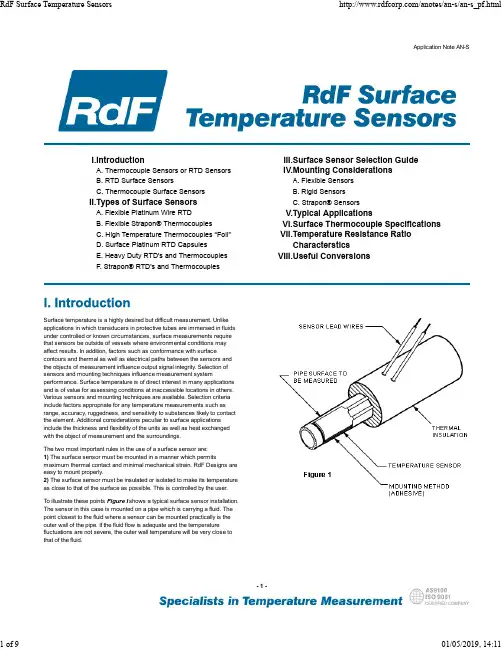
金龙STM32F207开发板用户手册
- 格式:pdf
- 大小:638.82 KB
- 文档页数:9
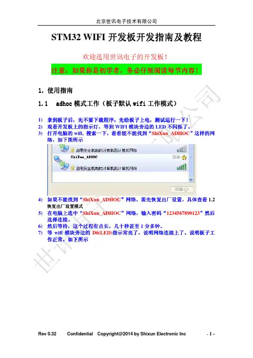
北京世讯电子技术有限公司STM32 WIFI 开发板开发指南及教程欢迎选用世讯电子的开发板! 注意: 注意:如果你是初学者, 如果你是初学者,务必仔细 务必仔细阅读 仔细阅读每节内容 阅读每节内容! 每节内容! 1. 使用指南1.1 adhoc 模式工作( 模式工作(板子默认 wifi 工作模式) 工作模式)拿到板子后, ,先不要下载程序, 1) 拿到板子后 先不要下载程序,先给板子上电, 先给板子上电,测试运行一下! 测试运行一下! 2) 观看开发板上的指示灯, 观看开发板上的指示灯,等到 WIFI 模块旁边的 LED 不闪烁了。
不闪烁了。
3) 打开电脑的 wifi, 搜索一下, 搜索一下,看看能不能找到“ 看看能不能找到“ShiXun_ADHOC”这样的网 络,如下图所示4) 如果不能找到“ 如果不能找到“ShiXun_ADHOC”网络, 网络,需先恢复出厂设置, 需先恢复出厂设置,具体查看 1.2恢复出厂设置模式5) 在电脑上选中“ 在电脑上选中“ShiXun_ADHOC”网络, 网络,输入密码“ 输入密码“1234567890123”然后 选择连接。
选择连接。
6) 然后等待, 然后等待,这个过程有点长, 这个过程有点长,几十秒甚至 几十秒甚至 1 分多钟。
分多钟。
7) 等 wifi 模块旁边的 D6(LED)指示常亮 指示常亮了 常亮了,说明网络连接上了。
说明网络连接上了。
说明板子工 作正常。
作正常。
如下所示Rev 0.32Confidential Copyright@2014 by Shixun Electronic Inc-1-北京世讯电子技术有限公司B. 显示分配到 IP A. 显示已经连接上 8) 打开浏览器, 打开浏览器,输入地址 http://192.168.10.10/ 就可以出来下面页面了9) 然后点击测试部分, 然后点击测试部分,继电器开、 继电器开、关,LED 灯开、 灯开、关。
STM32开发板使用说明1、开发板使用到的软件及安装说明在开始学习开发板之前需要安装的软件有:1、KEIL3.80A,2、PL-2303HX驱动,3、串口调试助手,4、下载器MCUISP。
这些软件在课件文件下面的软件文件里。
具体安装步骤如下:1.KEIL3.80A的安装,打开路径:课件\软件\KEIL3.80A\MDK3.80A安装手册,根据上面的步骤安装软件。
2.PL-2303HX驱动的安装,打开路径:课件\软件\PL-2303HX新版驱动,可根据使用电脑的操作系统来选择安装的软件,如选择安装XP驱动,可打开XP驱动,根据里面的安装说明来安装软件。
一般只要运行PL-2303 Driver Installer。
exe就可以了。
3.串口调试助手的安装,打开路径:课件\软件\串口调试助手,点击sscom33。
exe即可,也可以创建快捷方式在桌面。
4.下载器MCUISP的安装,打开路径:课件\软件\下载器MCUISP,点击mcuisp。
exe 即可,也可以创建快捷方式在桌面。
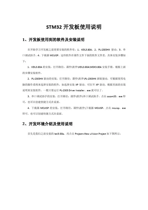
2、开发环境介绍及使用说明首先是我们之前安装的keil3.80a。
再点击Project->New uVision Project如下图所示:弹出create new project 对话框,新建一个文件夹TEST,然后把工程名字设为test。
点击保存。
弹出选择器件的对话框,因为我们的开发板使用的是STM32F103RBT6 ,所以在这里我们选择STMicroelectronics 下面的STM32F103RB( 如果使用的是其他系列的芯片,选择相应的型号就可以了)。
如下图所示:点击OK,MDK会弹出一个对话框,问你是否加载启动代码到当前工程下面,这里我们选择是。
启动代码是一段和硬件相关的汇编代码。
是必不可少的!在上面点击了是以后,MDK 就把启动代码STM32F10x。
s 加入到了我们的工程下面。
如下图所示:到这里,我们就可以开始编写自己的代码了。
金龙开发板网络例程说明文档硬件平台:金龙207开发板、金龙407开发板软件平台:固件库版本:1.0Freertos版本:6.1.0Lwip版本:1.3.2深圳旺宝电子实验一:Ping对于网络通信首先必须得保证网络连接正常,Ping命令是我们最常使用的检测网络的方法,将开发板与电脑用网线连接,首先我们需要对电脑进行如下配置,打开电脑网络,双击“本地连接”设置本地连接“属性”设置TCP/IP属性选择手动设置IP地址,这里设置为192.168.1.203,点击确定即可。
打开工程“金龙207网络之ping”。
打开main.h我们可以看出开发板IP地址为192.168.1.199,开发板IP地址与电脑IP地址必须在一个网段内(这里是192.168.1.xxx),如果不需要使用LCD显示(使用旺宝电子3.2寸触摸屏模块),可关掉宏“USE_LCD”。
STM32与DP83848采用的是RMII接口,STM32为DP83848提供50MHz时钟,使用宏“RMII_MODE”。
如下图为金龙207开发板照片,若网络灯不亮,请检查J8跳线帽是否连接(如下标注,需连接上),可用示波器测试此处波形频率为50MHz正弦波。
JLINK下载运行后,使用交叉网线将电脑与开发板连接,点击开始->运行输入cmd出现命令提示符界面,输入ping192.168.1.199,如下图,可以看到Reply from192.168.1.199: bytes=32time<1ms TTL=255则说明开发板与电脑连接正常。
LCD显示板卡IP地址,若不需要LCD显示可在main.h中将USE_LCD宏关掉。
实验二:TCP服务器本实验使用金龙207开发板作为TCP服务器,电脑作为TCP客户端进行通信。
初始化TCP服务器任务,创建TCP socket,绑定到本地端口8080,后循环开始监听端口,当有客户端连接后进入tcp_server_serve函数进行处理。
奔奔STM32F207入门学习笔记系列之一STM32F2x搭建开发环境本小节主要介绍STM32F2x系列芯片的开发环境搭建过程。
讲解之前先聊一下STM32F2x这个系列的芯片。
与之前的STM32F1x,主要有一下几点的优势:1)STM32F2x 的主频提升到了120MHZ,150DMIPS 处理速度。
内部RAM128+4K 内嵌Flash 1M。
2)外设丰富了很多。
增加了以下主力外设:Ethernet、USB OTG High/Full、DCMI数字摄像头。
3)对原来的外设有了增强。
比如:现在的RTC多了一个RTC的控制器,原来只是一个32位的定时器。
I2S原来只是半双工,现在是全双工,可以做多声道的播放器。
4)增加了芯片的安全加密性能。
在内部集成了AES/DES/CRC等硬件加密器,不需要软件算法来实现。
这点比较好。
5)在外设库方面,与F1不兼容了,有新的库文件提供。
库是越来越好了,嘿嘿方便我们开发。
暂时只说这么多,后面我们继续补充。
在国内主流的两种编译器为MDK以及IAR,本小节以MDK为例讲解开发环境的搭建。
硬件平台:深圳市天漠科技的STM32F207 开发板(DevKit1207)。
选择它的理由:1)功能很全面,基本上该有的功能都有了,方便我学习这款芯片。
大家可以测试基于 F2系列的基本上所有的功能。
2)它的器件选型时工业级,物料也比较好购买,我做项目的时候可以直接抄它的原理图---。
--本人有点小懒。
3)支持UCGUI3.90a以及uCOS-II,方便我做项目,其它一家的没有。
4)范例丰富,文档写的比较好。
以上是我自己买它的原因,仅供参考。
软件平台:MDK(即keil 4)F2系列的芯片至少需要MDK4.20以上版本支持,STM32F4需要MDK4.22A以上。
软件库以及范例。
基于天漠的DevKit1207提供的相关范例。
想在开始向大家讲解,怎么用KEIL 4创建一个新的工程,具体步骤如下:1)。
STM32F207的时钟说明请尽可能参阅英文原文件STM32F207有三个可选的时钟源,具体如下:(1)HIS时钟源(内部集成的时钟源)(2)HSE时钟源(外部高速晶体振荡器提供的时钟源或来自其他设备的时钟源)(3)PLL(PLL的时钟输入可以是HIS或者HSE时钟源)时钟控制器在选择内核及外设的时钟时具有高度的灵活性,以使他们都可以工作在最高频率上,并且能够保证给那些需要特殊频率的外设提供合适的频率,如Ethernet, USB OTG FS 和HS,I2S和SDIO。
三个可选的时钟源都可以独立地打开或关闭,以降低系统的功耗。
设备还有两个次要的时钟源,具体如下:(1)32KHz低速内部RC,可以驱动独立的看门狗和可以选择性使用的RTC(可用于在停止或待机状态下自动唤醒设备)(2)32.768KHz的低速外部晶体,可以作为RTC的时钟源。
几个预分频器用于配置AHB总线的频率,高速APB总线(APB2)和低速APB总线(APB1)所控制的区域的频率。
AHB总线的最高频率是120MHz,APB2总线的最高频率是60MHz,APB1总线的最高频率是30MHz。
所有的外设时钟都来源于系统时钟(SYSCLK),以下的几个除外:(1)USB OTG FS时钟(48MHz),随机模拟产生器(RNG)时钟(<=48MHz),SDIO时钟(<=48MHz),这些时钟来源于一个特殊的PLL(PLL2)的输出(PLL48CLK)。
(2)I2S时钟:为了达到高品质的音频效果,I2S时钟可能从特殊的PLL(PLLI2S)或外部接在I2S_CKIN引脚上的时钟得到。
(3)USB OTG HS(60MHz)时钟,由外部硬件提供。
(4)Ethernet MAC时钟(TX,RX和RMII)可以从外部硬件得到。
Ethernet使用时,AHB总线时钟不得低于25MHz。
RCC模块将AHB时钟8分频后提供给了Cortex系统定时器System Timer。
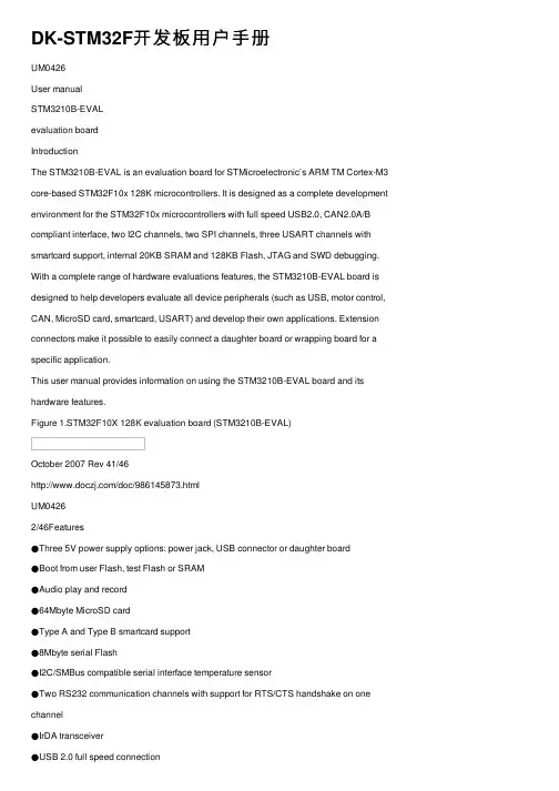
DK-STM32F开发板⽤户⼿册UM0426User manualSTM3210B-EVALevaluation boardIntroductionThe STM3210B-EVAL is an evaluation board for STMicroelectronic’s ARM TM Cortex-M3 core-based STM32F10x 128K microcontrollers. It is designed as a complete development environment for the STM32F10x microcontrollers with full speed USB2.0, CAN2.0A/B compliant interface, two I2C channels, two SPI channels, three USART channels with smartcard support, internal 20KB SRAM and 128KB Flash, JTAG and SWD debugging. With a complete range of hardware evaluations features, the STM3210B-EVAL board is designed to help developers evaluate all device peripherals (such as USB, motor control, CAN, MicroSD card, smartcard, USART) and develop their own applications. Extension connectors make it possible to easily connect a daughter board or wrapping board for a specific application.This user manual provides information on using the STM3210B-EVAL board and its hardware features.Figure 1.STM32F10X 128K evaluation board (STM3210B-EVAL)October 2007 Rev 41/46/doc/986145873.htmlUM04262/46Features●Three 5V power supply options: power jack, USB connector or daughter board●Boot from user Flash, test Flash or SRAM●Audio play and record●64Mbyte MicroSD card●Type A and Type B smartcard support●8Mbyte serial Flash●I2C/SMBus compatible serial interface temperature sensor●Two RS232 communication channels with support for RTS/CTS handshake on one channel●IrDA transceiver●USB 2.0 full speed connection●CAN 2.0A/B compliant connection●Induction motor control connector●JTAG, SWD and trace tool support●240x320 TFT color LCD●Joystick with 4-direction control and selector●Reset, wakeup, tamper and user push buttons● 4 LEDs●RTC with backup battery●Extension connector for daughter board or wrapping boardOrder codeTo order the STM32F10x 128K evaluation board, use the order code STM3210B-EVAL. UM0426ContentsContents1Hardware layout and configuration . . . . . . . . . . . . . . . . . . . . . . . . . . . . . 51.1LCD configuration . . . . . . . . . . . . . . . . . . . . . . . . . . . . . . . . . . . . . . . . . . . . 71.2Power supply . . . . . . . . . . . . . . . . . . . . . . . . . . . . . . . . . . . . . . . . . . . . . . . 91.3Boot option . . . . . . . . . . . . . . . . . . . . . . . . . . . . . . . . . . . . . . . . . . . . . . . . 101.4Clock source . . . . . . . . . . . . . . . . . . . . . . . . . . . . . . . . . . . . . . . . . . . . . . . 101.5Reset source . . . . . . . . . . . . . . . . . . . . . . . . . . . . . . . . . . . . . . . . . . . . . . 111.6Audio . . . . . . . . . . . . . . . . . . . . . . . . . . . . . . . . . . . . . . . . . . . . . . . . . . . . 111.7Serial flash . . . . . . . . . . . . . . . . . . . . . . . . . . . . . . . . . . . . . . . . . . . . . . . . 111.8CAN . . . . . . . . . . . . . . . . . . . . . . . . . . . . . . . . . . . . . . . . . . . . . . . . . . . . . 111.9RS232 . . . . . . . . . . . . . . . . . . . . . . . . . . . . . . . . . . . . . . . . . . . . . . . . . . . 121.10Motor control . . . . . . . . . . . . . . . . . . . . . . . . . . . . . . . . . . . . . . . . . . . . . . 121.11Smartcard . . . . . . . . . . . . . . . . . . . . . . . . . . . . . . . . . . . . . . . . . . . . . . . . . 131.12MicroSD card . . . . . . . . . . . . . . . . . . . . . . . . . . . . . . . . . . . . . . . . . . . . . . 131.13Temperature sensor . . . . . . . . . . . . . . . . . . . . . . . . . . . . . . . . . . . . . . . . . 131.14Analog input . . . . . . . . . . . . . . . . . . . . . . . . . . . . . . . . . . . . . . . . . . . . . . . 131.15IrDA . . . . . . . . . . . . . . . . . . . . . . . . . . . . . . . . . . . . . . . . . . . . . . . . . . . . . 141.16USB . . . . . . . . . . . . . . . . . . . . . . . . . . . . . . . . . . . . . . . . . . . . . . . . . . . . . 141.17Development and debug support . . . . . . . . . . . . . . . . . . . . . . . . . . . . . . . 141.18Display and input devices . . . . . . . . . . . . . . . . . . . . . . . . . . . . . . . . . . . . . 152Connectors . . . . . . . . . . . . . . . . . . . . . . . . . . . . . . . . . . . . . . . . . . . . . . . 162.1USB type B connector CN1 . . . . . . . . . . . . . . . . . . . . . . . . . . . . . . . . . . . 162.2CAN D-type 9-pin male connector CN2 . . . . . . . . . . . . . . . . . . . . . . . . . . 162.3Analog input connector CN3 . . . . . . . . . . . . . . . . . . . . . . . . . . . . . . . . . . 172.4Power supply connector CN4 . . . . . . . . . . . . . . . . . . . . . . . . . . . . . . . . . . 172.5RS232 connector CN5 with RTS/CTS handshake support . . . . . . . . . . . 182.6RS232 connector CN6 . . . . . . . . . . . . . . . . . . . . . . . . . . . . . . . . . . . . . . 182.7JTAG debugging connector CN7 . . . . . . . . . . . . . . . . . . . . . . . . . . . . . . . 192.8Audio jack CN8 . . . . . . . . . . . . . . . . . . . . . . . . . . . . . . . . . . . . . . . . . . . . . 192.9SWD debugging connector CN9 . . . . . . . . . . . . . . . . . . . . . . . . . . . . . . . 192.10Trace debugging connector CN10 . . . . . . . . . . . . . . . . . . . . . . . . . . . . . . 203/46Contents UM04264/462.11Daughter board extension connectors CN12 and CN13 . . . . . . . . . . . . . 21 2.12Motor control connector CN14 . . . . . . . . . . . . . . . . . . . . . . . . . . . . . . . . . 24 2.13MicroSD connector CN15 . . . . . . . . . . . . . . . . . . . . . . . . . . . . . . . . . . . . . 26 2.14Smartcard connector CN16 . . . . . . . . . . . . . . . . . . . . . . . . . . . . . . . . . . . 263Schematics . . . . . . . . . . . . . . . . . . . . . . . . . . . . . . . . . . . . . . . . . . . . . . . 28 Appendix A STM3210B-EVAL IO assignments . . . . . . . . . . . . . . . . . . . . . . . . . . 41 Revision history . . . . . . . . . . . . . . . . . . . . . . . . . . . . . . . . . . . . . . . . . . . . . . . . . . . . 45UM0426Hardware layout and configuration 1 Hardware layout and configurationThe STM3210B-EVAL board is designed around a STM32F103VBT6 microcontroller in a100-pin LQFP package.The hardware block diagram Figure2 shows the connections between the STM32F10xmicrocontroller and peripherals (LCD, SPI Flash, USART, IrDA, USB, Audio, CAN bus, RTC,smartcard, MicroSD card and motor control).Figure3will help you locate these features on the evaluation board.5/46Hardware layout and configuration UM04266/46Figure 3.STM3210B-EVAL board layoutCN12Extension connectorCN5USART2U1STM32F103VBT6CN6USART1U11IrDACN1USBCN45V powerB1RESET B2WAKEUP CN16Smartcard B4T amper U18JoystickB3General purpose keyCN14Motor controlCN2CAN connectorCN9SWDCN10T raceCN7JT AGU17Color LCDCN8Audio jackRV1PotentiometerCN13Extension connectorCN15MicroSD cardUM0426Hardware layout and configuration7/46The following sections provide jumper settings for configuring your STM3210B-EVAL board and peripherals.Two types of jumpers are used on the STM3210B-EVAL board:●3-pin jumpers with two possible positions, for which the possible settings are presented in schematics in the following sections●2-pin jumpers with two possible settings: Fitted – the circuit is closed, and Not fitted – the circuit is open (see Figure 4.) Figure 4.Settings for two-pin jumpersconfigurationThe STM3210B-EVAL can be delivered with either one of two LCDs mounted on the MB542board, depending on the board version. These two LCDs look alike and operate in the same way, however they have different control circuits, and therefore require different software drivers. Y ou must ensure that the demonstration software pre-loaded in the flash memory of the microcontroller on the evaluation board supports the LCD that you have.If your STM3210B-EVAL product includes the MB542 board version B-01 or later , it is mounted with the LCD referenceAM240320L8TNQW-00H (from Ampire). The controller reference is ILI9320 (from ILITEK,/doc/986145873.html). The products that include this LCD have a label on the daughter board (to the left of the display) as shown in Figure5.Figure 5.LCD label on MB542 board version B-01 or laterNot fittedFittedHardware layout and configurationUM04268/46The demonstration software delivered with the evaluation boards that carry this label is STM3210B-EVAL_DEMO version 1.1 or later. It automatically detects which version of the LCD is mounted on the daughter board, and it supports both.If your STM3210B-EVAL product includes the MB542 board version B-00 or earlier , it is mounted with the LCD reference AM-240320LTNQW01H. The controller reference is HX8312-A (from Himax, /doc/986145873.html ). The products that include this LCD do not have a label on the component side of the daughter board as shown in Figure 6. The label is on the solder side, therefore not visible when the MB452 board is screwed onto the MB525 board.Figure 6.No LCD label on component side of MB542 board version B-00The demonstration software delivered with the evaluation boards that do not carry a visible label is STM3210B-EVAL_DEMO version 1.0 or earlier. This software only supports the LCD reference AM-240320LTNQW01H.Note:Y ou can download the latest version of the software demonstration from theSTmicroelectronics support site, /doc/986145873.html/mcu. The STM3210B-EVAL_DEMO software is included in the STM3210B-EVAL demonstration software user manual (UM0435)download file. STM3210B-EVAL_DEMO version 1.1 and later support both types of LCD.Table 1.LCD label on MB542 board version B-01 or laterLabel markingMeaningMB542B-0120743001LCD version B-01B PCB version B 01Version 0120743001Board IDUM0426Hardware layout and configuration9/461.2 Power supplyThe STM3210B-EVAL board is designed to be powered by 5V DC power supply and to beprotected by PolyZen U6 in case of incorrect power supply configuration. It is possible to configure the evaluation board to use any of the following sources for the power supply.●5V DC power adapter connected to CN4, the power supply jack labeled “PSU” (for Power Supply Unit) on the silkscreen ●5V DC power with 500mA limitation from CN1, the type-B USB connector on the evaluation board labeled “USB” on the silkscreen●5V DC power from both CN12 and CN13, the daughter board extension connectors labeled “DTB” (for Daughter Board) on the silkscreenThe power supply is configured by setting the related jumpers JP4, JP9 and JP11 as described in T able 2.The LED LD5 is lit when the STM3210B-EVAL board is powered correctly.Hardware layout and configuration UM042610/461.3 Boot optionThe STM3210B-EVAL board is able to boot from:●Embedded user Flash●System memory with boot loader for ISP ●Embedded SRAM for debuggingThe boot option is configured by setting the switches SW1 and SW2 as shown in Table 3.The two possible positions of these micro switches are shown in Figure 7.Figure 7.Switch positions1.4 Clock sourceTwo clock sources are available on the STM3210B-EVAL board for the STM32F10Xmicrocontroller and RTC.●X1, 32KHz crystal for embedded RTC●X2, 8MHz crystal with socket for the STM32F10X microcontroller. It can be removed from the socket when the internal RC clock is used.Table 3.Boot switchesSwitchBoot fromSwitch configurationSTM3210B-EVAL boots from user Flash when SW2 is set as shown to the right (default setting).In this configuration, the position of SW1 doesn’t affect the boot process.Boot 0 = 0, Boot 1 = XSTM3210B-EVAL boots from embedded SRAM when SW1 and SW2 are set as shown to the right. Boot 0 = 1, Boot 1 = 1 STM3210B-EVAL boots from system memory when SW1 and SW2 are set as shown to the right.Boot 0 = 1, Boot 1 = 01 <> 0Switch in position “1”Switch in position “0”1 <> 0S W 1B o o t 1S W 2B o o t 01 <> 0S W 1B o o t 1S W 2B o o t 01 <> 0S W 1B o o t 1S W 2B o o t 0UM0426Hardware layout and configuration11/461.5 Reset sourceThe reset signal of the STM3210B-EVAL board is active low and the reset sources include:●Reset button B1●Debugging tools from connector CN7, CN9 and CN10●Daughter board from CN131.6 AudioThe STM3210B-EVAL board supports both audio recording and playback. This can bedisabled or enabled by setting the jumpers JP6 and JP7. The audio volume can be adjusted using the potentiometer RV2, and the microphone amplifier gain can be adjusted using the potentiometer RV3.1.7 Serial flashA 64Mbit serial flash connected to SPI1 of the STM32F10X microcontroller shares the sameSPI port with the MicroSD card using a different chip select signal. Serial Flash Chip select is managed by the standard IO port PA4.1.8 CANThe STM3210B-EVAL board supports CAN 2.0A/B compliant CAN bus communication based on 3.3V CAN transceiver. The high-speed mode, standby mode and slope control mode are available and selected by setting JP2.Table 4.Reset jumperDescriptionJP10Enables reset of the STM32F10X microcontroller embedded JT AG T AP controllereach time a system reset occurs. JP10 connects the TRST signal from the JT AG connection with the system reset signal RESET#.Default setting: Not fittedTable 5.Audio jumpersJumper DescriptionJP6Audio power amplifier TS4871 is forced into standby mode when JP6 is not fitted. Default setting: FittedJP7Microphone pre-amplifier MAX4061 is forced into shutdown mode when JP7 is fitted. Default setting: Not fittedHardware layout and configurationUM042612/461.9 RS232Two Type D 9-pin connectors, CN6 (USART1) and CN5 (USART2) are available on the STM3210B-EVAL board. The USART1 connector is connected to the RS232 transceiver U10, and the USART2 connector with RTS/CTS handshake signal support is connected to the RS232 transceiver U9.1.10 Motor controlThe STM3210B-EVAL board supports induction motor control via a 34-pin connector, CN14,which provides all required control and feedback signals to and from a motor power-drive board. Available signals on this connector include emergency stop, motor speed, 3-phase motor current, bus voltage, heatsink temperature coming from the motor drive board and 6 channels of PWM control signals going to the motor drive circuit.Special motor current sampling operation is enabled by setting jumper JP8.Table 7.Motor control jumpersJumperDescriptionJP8Enables special motor current sampling operation when JP8 is fitted (PD2 connected to PB0). The IO pins PD2 and PB0 are disconnected and can be used by the daughter board when JP8 is not fitted.Default setting: FittedJP12JP12 must be open when the digital encoder signal comes from pin31 of CN14. It must be closed when an analog signal comes from pin31 of CN14.Default setting: Not fitted (open)UM0426Hardware layout and configuration13/461.11 SmartcardThe STMicroelectronics smartcard interface device ST8024 is used on the STM3210B-EVAL board for asynchronous 3V and 5V smartcards. It performs all supply protection and control functions based on the connections with the STM32F10X microcontroller, which are listed in Table 8.An example of smartcard is provided with the board called GSM file system sample . With this board, you can play basic commands, select a file and do simple read/write operations to become familiar with this interface and the ISO/IEC 7816-3 protocol.1.12 MicroSD cardThe 64Mbyte or 128Mbyte MicroSD card, which is connected to SPI1 of the STM32F10xmicrocontroller (shared with serial Flash), is available on the board. The MicroSD card chip selection is managed by the standard IO port PC12.1.13 Temperature sensorOne I 2C interface temperature sensor STLM75 (–55°C to +125°C), which is connected toI 2C1 of the STM32F10x microcontroller, is available on the board. Two discrete N-channel enhancement MOS-FETs are used to demonstrate how different voltage level devices can be connected to the same I 2C bus.1.14 Analog inputOne BNC connector, CN3, is connected to PC1, the ADC channel 11 of the STM32F10xmicrocontroller as an external analog input.Table 8.Connection between ST8024 and STM32F10XST8024 signals DescriptionConnect to STM32F10X5V/3V Smartcard power supply selection pin PD11I/OUC MCU data I/O linePB10XT AL1Crystal or external clock inputPB12OFF Detect presence of a card, Interrupt to MCU PE14RSTIN Card reset input from MCUPB11CMDVCCStart activation sequence input (active low)PE7Hardware layout and configuration UM042614/461.15 IrDAIrDA communication is supported by the IrDA transceiver U11, which is connected to USART3 of the STM32F10x microcontroller. It can be enabled or disabled by setting the jumper JP5.1.16 USBThe STM3210B-EVAL board supports USB2.0 compliant full-speed communication via a USB type B connector (CN1). The evaluation board can be powered by this USB connection at 5V DC with a 500mA current limitation. USB disconnect simulation can be implemented by disconnecting a 1.5K pull-up register from the USB+ line. The USB disconnect simulation feature is enabled by setting JP1.1.17 Development and debug supportThe following debug connectors are available on the STM3210B-EVAL board:●CN7, an industry standard 20-pin JTAG interface connector for connection of debugging/programming tools for ARM7 and ARM9 core-based devices.●CN9, a 10-pin SWD debug connector that supports the new Serial Wire Debug feature of ARM Cortex-M3 devices.●CN10, a 20-pin connector for legacy and future JTAG tools that are compliant with ARM CoreSight.Table 9.IrDA jumpersJumper DescriptionJP5Enables/disables the IrDA transceiver. IrDA is enabled when JP5 is fitted, and disabled when JP5 is not fitted.Default setting: FittedUM0426Hardware layout and configuration15/461.18 Display and input devicesThe 240x320 TFT color LCD (U17) and 4 general purpose LEDs (LD1, 2, 3, 4) are available as display devices. A 4-direction joystick with selection key, general purpose pushbutton (B3), wakeup button (B2) and tamper detection button (B4) are available as input devices.The STM3210B-EVAL board also supports a second optional 122x32 graphic LCD that can be mounted on the U19 connector. The graphic LCD is not provided.Table 11.LCD modulesGraphic LCD U17 (default)Character LCD U19 (optional)Pin on U17Description Pin connectionPin on U19DescriptionPin connection1CS PB21Vss GND 2SCL PB132Vcc +3.3V 3SDI PB153VO -4RS PD74CLK PB135WR PD155SID PB156RD GND 6CS PB27SDO PB147A +5V 8RESET#RESET#8KGND9VDD +3V310VCI +3V311GND GND 12GND GND 13BL_VDD +3V314BL_Control PA815BL_GND GND 16BL_GNDGNDConnectors UM0426 2 Connectors2.1 USB type B connector CN1Figure /doc/986145873.htmlB type B connector CN1 (front view)Table 12. USB type B connector (CN1)Pin number Description Pin number Description1VBUS(power)4GND2DM5, 6Shield3DP2.2 CAN D-type 9-pin male connector CN2Figure 9.CAN D-type 9-pin male connector CN2 (front view)Table 13.CAN D-type 9-pin male connector (CN2)Pin number Description Pin number Description1, 4, 8, 9NC7CANH2CANL3,5,6GND16/46UM0426Connectors17/462.3 Analog input connector CN3Figure 10.Analog input connector CN3 (top view)2.4 Power supply connector CN4The STM3210B-EVAL board can be powered from a DC 5V power supply via the external power supply jack (CN4) shown in Figure 11. The central pin of CN4 must be positive.Figure 11.Power supply connector CN4 (front view)Table 14.Analog input connector CN3Pin numberDescription Pin numberDescription1GND 4GND2GND 5Analog input/PC13GND1453 2DC +5VGNDConnectors UM0426 2.5 RS232 connector CN5 with RTS/CTS handshake support Figure 12.RS232 connector CN5 with RTS/CTS handshake support (front view)Table 15.RS232 connector CN5 with full modem control supportPin number Description Pin number Description1NC6Connect to Pin 42USART2_RXD7USART2_RTS3USART2_TXD8USART2_CTS4Connect to Pin 6 9NC5GND2.6 RS232 connector CN6Figure 13.RS232 connector CN6 (front view)Table 16.RS232 connector CN6Pin number Description Pin number Description1NC6Connect to Pin 42USART1_RXD7Connect to Pin 83USART1_TXD8Connect to Pin 74Connect to Pin 69NC5GND18/46UM0426Connectors 2.7 JTAG debugging connector CN7Table 17.JTAG debugging connectorPin number Description Pin number Description1 3.3V power2 3.3V power3TRST4GND5TDI6GND7TMS8GND9TCK10GND11RTCK12GND13TDO14GND15RESET#16GND17DBGRQ18GND19DBGACK20GND2.8 Audio jack CN8A 3.5mm mono audio jack CN8 is available on the STM3210B-EVAL board. The speaker U12 is bypassed when earphones are plugged into CN8.2.9 SWD debugging connector CN919/46。
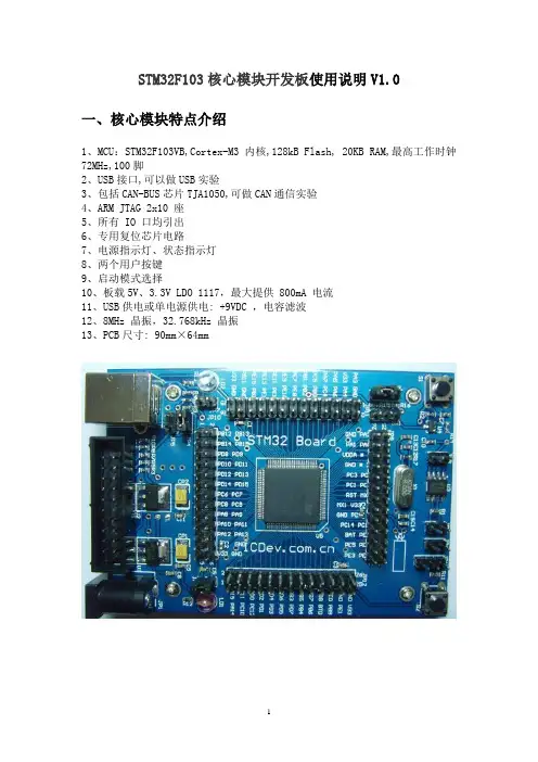
STM32F103核心模块开发板使用说明V1.0一、核心模块特点介绍1、MCU:STM32F103VB,Cortex-M3内核,128kB Flash, 20KB RAM,最高工作时钟72MHz,100脚2、USB接口,可以做USB实验3、包括CAN-BUS芯片TJA1050,可做CAN通信实验4、ARM JTAG 2x10 座5、所有 IO 口均引出6、专用复位芯片电路7、电源指示灯、状态指示灯8、两个用户按键9、启动模式选择10、板载5V、3.3V LDO 1117,最大提供 800mA 电流11、USB供电或单电源供电: +9VDC ,电容滤波12、8MHz 晶振,32.768kHz 晶振13、PCB尺寸: 90mm×64mm二、跳线说明1、启动方式选择跳线说明开发板上的启动方式选择跳线R16100KV33231SW2BOOT0R15100KV33231SW1PB2启动方式选择跳线对应的原理图SW1和SW2为STM32启动方式选择跳线,当SW2左边两个插针短接(即中间插针BOOT0与GND 短接),SW1不接任何跳线帽时,为从FLASH 启动模式,正常使用开发板时,此跳线需短接,如上图所示。
当SW1左边两个插针短接(即中间插针PB2与GND 短接,1和2短接),SW2不接任何跳线帽时,为System Memory 模式。
2、其他跳线说明 (1) JP4和JP5开发板上的JP4和JP5跳线JP4和JP5跳线对应的原理图如上图所示,JP4短接后可以通过USB接口给开发板供电,JP5用来选择是否给PA12(D+)提供1.5k电阻的上拉,做USB相关实验时,需短接。
(2) JP8跳线开发板上的JP8跳线V33VDDAJP8跳线对应的原理图JP8跳线用来给STM32芯片的模拟电源选择供电电源,通常情况下,JP8跳线需短接,用+3.3V提供电源。
(3) JP9双排针(4) JP10双排针(5) JP11双排针(6) JP12双排针三、IAR下用Jlink调试STM32核心模块开发板确认SW2,JP8,JP4,JP5跳线正确短接后,开始安装IAR软件,安装EWARM-EV-WEB-511后,在安装后的目录里\Program Files\IAR Systems\Embedded Workbench 5.0 Evaluation\ARM\examples\ST\STM32F10x\IAR-STM32-SK ,打开IAR-STM32-SK.eww文件,它里面包含多个工程,除了LCD_Demo外,其它工程均无需改动,可以直接使用JLINK下载调试。
STM32在MDK中使用外部RAM浅解使用简介:开发板神舟王STM32F207 开发板问题描述:在使用emwin 的时候由于占用的变量较多,出现了STM32F207 内部RAM 不够用的尴尬局面,开发板自带了4M 的外部SRAM,因此考虑速度和存储的平衡,使用芯片内部RAM 作为堆栈区使用,外部RAM 则用来存储其他变量修改内容:启动文件即startup_stm32f2xx.s 文件1.添加标志量:DATA_IN_ExtSRAM EQU 1 ;主要是方便控制切换使用内部和外部RAM2.修改栈区:IF DATA_IN_ExtSRAM == 1__initial_sp EQU 0x20000000 + Stack_Size ELSE__initial_spENDIF3.在进入main 函数之前初始化外部RAM 有两种初始化方式第一种:在SystemInit 内初始化SystemInit 函数位于system_stm32f2xx.c 文件内定义宏变量DATA_IN_ExtSRAM 这样系统初始化时就会调用函数SystemInit_ExtMemCtl 修改SystemInit_ExtMemCtl 函数内容,即初始化FSMC RAM 第二种在startup_stm32f2xx.s 内调用main 函数前先调用RAM 初始化函数完成RAM 的初始化IMPORT __main IMPORT SystemInit IMPORT SRAM_Init LDR R0, =SystemInit BLX R0LDR R0, =SRAM_Init BLX R0 LDR R0, =__main BX R0 ENDP 当然还有最蛋疼的一种方式就是在startup_stm32f2xx.s 初始化外部RAM 不过需要修改成汇编语言最后就是修改MDK 的配置在option->target 勾选上外部RAM 之后就可以尝试定义一个大数组试试了tips:感谢大家的阅读,本文由我司收集整编。
STM32核心板用户手册编著:产品部2013年10月4日目录1软件安装 (1)1.1JLink驱动 (1)1.2MDK3.8A (3)1.3PL-2303HX驱动 (8)1.4本章小结 (9)2工程 (10)2.1新建工程 (10)2.2编译工程 (16)2.3下载测试 (18)2.3.1串口下载 (18)2.3.2JTAG下载 (22)1软件安装本章节主要介绍几款软件的安装,打开“stm32核心板资料\软件”,就能看见如下几个文件夹(如图1.1)。
图1.1五款软件文件夹1.1JLink驱动双击“JLINK驱动”文件夹,如图1.1.1,左边为JLink软件说明,右边问软件安装包。
图1.1.1“JLINK驱动”文件夹内容现在我们开始安装JLink驱动,双击右边图标,如下图图1.1.2。
图1.1.2点击“YES”或“NEXT”就可以完成驱动安装。
图1.1.3安装进度此软件安装时间是比较短的,安装进程完成后会直接跳入下一个窗口,点击“Finish”后,此软件就安装好了。
将JLink插入电脑的USB端口,会听到提示音,打开设备管理器,就可以查看到电脑是否识别此设备了。
如图1.1.4。
图1.1.4识别J-Link查找到J-Link driver,说明驱动已近安装好。
1.2MDK3.8AMDK3.8A,我们用它作为我们的编译器,此软件安装好后需要注册,如果不注册,编译的工程过大时,编译就会出现问题。
好了,下面我们就开始软件安装与注册。
打开文件夹MDK3.8A,就可以看到下面几个文件,如图1.2.1:图1.2.1“MDK3.8A”文件夹下内容双击第一个文件,开始我们的软件安装。
双击后如图1.2.2:图1.2.2开始安装点击“Next”。
图1.2.3小方框内打“勾”,点击“Next”;图1.2.4选择软件安装路径,点击“Next”;图1.2.5安装窗口提示,填写适当内容。
点击“Next”;图1.2.6这款软件安装的时间相对长一些,请耐心等待一下。
STM32主机使用说明书一、介绍纳英特STM32智能机器人平台采用ST公司的STM32103FVET6作为主控制器,内核采用了ARM公司Cortex M3存储容量大、运行速度快、外围接口丰富、稳定可靠,支持图形化及C语言编程,同时兼容原配件,是您进行竞赛、教学的理想选择。
二、布局(根据盒子图片再做)三、操作3.1搭建根据需要搭建机器人整机,连接传感器与马达,连接马达等,具体搭建方法请参考相应的项目手册,如灭火、足球项目的不同方案。
3.2编程根据项目需要对机器人进行编程。
可使用图形化的积木式编程模式,也可以使用C语言模式,软件的使用方法请参阅《纳英特积木式编程系统使用说明书》。
3.3下载软件上编程完成,编译通过,要下载时先把数据线连接好,再开启电源,这时主机会自动进入下载模式,被电脑识别为一个U盘,然后在软件上点击下载即可。
注:下载过程其实是将软件编译好的可执行文件***.bin文件拷贝到主机的这个U盘中,可执行的文件名是8.3格式的短文件名,不支持中文。
当软件新建的项目名为中文名时,下载时软件会跳出一个另存为的对话框,以英文或数字命名存储到U 盘即可;当项目名为英文或数字时,生成的***.bin文件的文件名即为项目名。
3.4运行程序下载完后,会保存在主机的U盘中,可同时存多个程序。
运行时,选择所需要的运行的程序名称即可。
主机开机后,屏幕上显示4个菜单选项,可通过上下键选择。
第一项为“运行”,后面显示的是当前的程序文件名,如果要运行的程序就是当前显示的程序,直接按确认键即可;如果要运行的程序不是当前显示的程序,则进入“选择程序”一项,屏幕会显示U盘中所存在的每一个程序名,通过上下键选择要运行的程序按确认键返回到原来的界面,再选择“运行”,按确认键。
3.5调试观察机器人运行结果是否符合预期的要求,如不符合,可重复以上4个步骤反复调试,直到符合预期的要求。
四、测试和设置主机固件中包含一个硬件的测试和设置的程序,在开机后的界面中选择“测试设置”,按确认键进入,屏幕显示“测试程序”,“参数修改”,“蓝牙设置”,“系统信息”。
Page 1基于ARM内核的32位MCU,150DMIPs,高达1MB Flash/128+4KB RAM,USB On-The-Go Full-speed/High-speed,以太网,17 TIMs,3 ADCs,15个通信&摄像头接口主要特性:内核:使用ARM 32位Cortex™-M3 CPU,自适应实时加速器(ART加速器™)可以让程序在Flash中以最高120MHz频率执行时,能够实现零等待状态的运行性能,内置存储器保护单元,能够实现高达150DMIPS/1.25DMIPS/MHz(Dhrystone 2.1)性能。
存储器:高达1M字节的Flash存储器512字节的动态口令存储器高达128+4K字节的SRAM灵活的静态存储控制器,支持CF卡、SRAM、PSRAM、NOR和NAND存储器并行LCD接口,兼容8080/6800模式时钟、复位和电源管理:1.65~3.6V用于供电和I/O管脚上电复位、掉电复位、可编程电压监测器和欠压复位4~26MHz晶体振荡器内嵌经出厂调校的16MHz RC振荡器(25 °C下精度为1%)带校准功能的32kHz RTC振荡器内嵌带校准功能的32kHz的RC振荡器低功耗:睡眠、停机和待机模式VBAT为RTC,20×32位后备寄存器,以及可选的4KB后备SRAM供电3×12位A/D转换器,0.5μs转换时间:多达24个输入通道在三倍间插模式下转换速率高达6MSPS2×12位D/A转换器通用DMA:16组带集中式FIFO和支持分页的DMA控制器多达17个定时器:多达12个16位和2个32位的定时器,频率可达120MHz,每个定时器有多达4个用于输入捕获/输出比较/PWM或脉冲计数的通道和增量编码器输入调试模式:串行单线调试(SWD)和JTAG接口Cortex-M3内嵌跟踪模块(ETM)多达140个具有中断功能的I/O端口:多达136个快速I/O端口,其频率可达60MHz多达138个耐5V的I/O端口多达15个通信接口:多达3个I2C接口(支持SMBus/PMBus)多达4个USART接口和2个UART接口(传输速率7.5 Mbit/s,支持ISO7816,LIN,IrDA接口和调制解调控制)多达3个SPI接口(传输速度可达30 Mbit/s),其中2个可复用为I2S接口,通过音频PLL或外部PLL来实现音频类精度2个CAN接口(2.0B 版本)SDIO接口高级互连功能:带有片上物理层的USB 2.0全速设备/主机/On-The-Go控制器带有专用DMA,片上全速PHY和ULPI的USB 2.0高速/全速设备/主机/On-The-Go 控制器带有专用DMA的10/100 以太网MAC.,支持硬件IEEE 1588v2(MII/RMII)8到14bit并行摄像头接口,最高达48Mbyte/sCRC计算单元96位唯一ID模拟真正的随机数发生器Page 2目录略Page 3目录略Page 4目录略Page 5表格目录略Page 6表格目录略Page 7插图目录略Page 8插图目录略Page 9插图目录略Page 101 简介这个数据手册给出了STM32F205xx和STM32F207xx系列微控制器的说明书。
1.概述金龙STM32开发板用户手册芯片描述-ARM32-bit Cortex-M3CPU-120MHz maximum frequency,150DMIPS/1.25DMIPS/MHz-Memory protection unitMemories-Up to1Mbyte of Flash memory-Up to128+4Kbytes of SRAM-Flexible static memory controller(supports Compact Flash,SRAM,PSRAM,NOR,NAND memories)-LCD parallel interface,8080/6800modesClock,reset and supply management-1.8to3.6V application supply and I/Os-POR,PDR,PVD and BOR-4to25MHz crystal oscillator-Internal16MHz factory-trimmed RC-32kHz oscillator for RTC with calibration-Internal32kHz RC with calibrationLow power-Sleep,Stop and Standby modes-VBAT supply for RTC,C32bit backup registers20optional4KB backup SRAMC12-bit,0.5us A/D converters3-up to24channels-up to6MSPS in triple interleaved modeC12-bit D/A converters2General-purpose DMA-16-stream DMA controllercentralized FIFOs and burst supportUp to17timers-Up to twelve16-bit and two32-bit timersDebug mode-Serial wire debug(SWD)&JTAG interfaces-Cortex-M3Embedded Trace MacrocellUp to140fast I/O ports with interrupt capability-51/82/114/140I/Os,all5V-tolerantUp to15communication interfacesC I2C interfaces(SMBus/PMBus)-Up to3-Up to6USARTs(7.5Mbit/s,ISO7816interface,LIN,IrDA,modem control)-Up to3SPIs(30Mbit/s),2with muxed I2S to achieve audio class accuracyC CAN interfaces(2.0B Active)-2-SDIO interfaceAdvanced connectivity-USB2.0FS device/host/OTG controller with on-chip PHY-USB2.0HS/FS device/host/OTG controller with dedicated DMAon-chip FS PHY and ULPI-10/100Ethernet MAC with dedicated DMAsupports IEEE1588v2hardware,MII/RMII8-to14-bit parallel camera interface-up to27Mbyte/s at27MHz or48Mbyte/s at48MHzCRC calculation unit,96-bit unique ID推荐理由:金龙STM32开发板采用意法半导体(ST)公司推出基于ARM CortexM3内核的STM32F207增强型系列芯片。
板上资源丰富,具有以太网(Ethernet)接口、USB从机(Device)、摄像头模块接口、TFT LCD、串口(UASRT)、I2C、SPI、AD、DA、PWM、CAN/485。
颇具特色的设计理念加上丰富的例程(均提供源代码)使得金龙STM32开发板非常适合初学者学习入门和项目评估使用。
板上资源:●支持一个TFT彩色液晶屏(需要另外搭配),搭配 2.8寸TFT真彩触摸屏模块或 3.2寸TFT真彩触摸屏模块大屏幕320*240,26万色TFT-LCD或4.3寸24位真彩触摸屏模块(由用户选择)大屏幕480*272或7寸16位真彩触摸屏模块(由用户选择)大屏幕800*480,支持8/16位总线接口,镜面屏,超高高度,FSMC控制,彩屏模块上配置ADS7843触摸控制器,支持一个SD卡(SPI方式)可用于存储图片、数据等,支持一个AT45DBxxx的DATA FLASH(可用于存储汉字库和图片或数据等)。
●一个以太网接口,板载美国国家公司高性能专用网络接口DP83848以太网控制芯片●一个USB从机接口(STM32FT6207VG芯片内置)●一路CAN、通信接口,驱动器芯片SN65VHD230)●一路485通信接口,驱动器芯片SP485EE●一路USB转RS232接口,驱动芯片PL2303HX●一个SD卡座SDIO方式控制方式●一个I2C存储器接口,标配24LC02(EEPROM)●一个SPI存储器接口,标配AT45DB161D(DATA FLASH){LCD模块上}●一路ADC调节电位器输入●两路ADC输入接线端子引出●两路DAC输出接线端子引出●四个个用户LED灯、一个电源指示灯,一个USB通信指示灯,两个用户按键,一个五向摇杆按键,一个系统复位按键,一个电源开关●一个摄像头模块接口●一个3.2、2.8、4.3寸屏幕接口●所有I/O口通过2.54MM标准间距引出,方便二次开发●板子规格尺寸:13CM X7.8CM2.电路及接口说明2.1Power supply(电源供给)金龙开发板采用外部5V电源输入、USB接口提供5V电源输入不需要跳线帽选择2.2Boot option(启动选项)金龙开发板可以采用以下几种启动方式:●Embedded user Flash(默认)●System memory with boot loader for ISP●Main Flash memory启动方式BOOT1(J1)BOOT0(J6)启动模式描述ANY(1-2、2-3or open)2-3金龙开发板设定为User Flash启动方式。
BOOT1可以任意位置,如插到1-2、2-3或是开路(既不插)默认是插到2-3(Defaultsetting)2-31-2金龙开发板设定为System Memory启动方式。
1-21-2金龙开发板设定为Embedded SRAM启动方式。
■Embedded user Flash(默认)默认配置好的,直接可以使用■System memory with boot loader for ISP打开flash loader demonstrator软件,按照如下方试配置好后上电后usb插在USB-232按下RESET 按键松开RESET然后点击NEXT选择好hex文件后点击next然后点击close,点击RESET后可以看到烧写的程序正常运行2.3Clock source(时钟源)金龙开发板由五个时钟源提供系统时钟、RTC时钟、USB HOST时钟、以太网时钟、MP3时钟。
Y1,25MHZ晶震,源做为系统的时钟源Y2,32.768kHZ晶震,做为RTC的时钟源.Y3,25MHZ晶震,网卡时钟,一般采样网卡自身时钟Y4,10MHZ晶震,usb转串口时钟2.4、复位方式复位信号在金龙开发板上是低电平复位。
复位方式包括以下几种方式:复位按键Reset通过JTAG仿真下载口输入复位信号2.5模拟输入STM32F207VG的外部模拟输入引脚PA4、PA5上,由AD5与AD4引出。
AD调节电位器输入VR1连接到PA4。
2.6DAC输出DAC连接到STM32F207VG的DAC输出引脚PA4、PA5,由DAC2与DAC1引出。
2.8USB-DEVICE/OTG金龙开发板提供了1个全速USB2.0设备端口,通过标准的USB-B型连接器引出。
通过该连接器,可以由PC给目标供电(最大电流500mA限制)。
2.9显示接口金龙开发板的P5接口可以连接一个2.8或3.2寸的320X240TFT彩色LCD,4.3寸24位真彩色;表4、彩色TFT LCD接口描述引脚定义如下:2.10EEPROM金龙开发板外接一个24LC02EEPROM连接到STM32F207VG的I2C1总线上,PB6接EEPROM的SCL,PB7接EEPROM的SDA。
跳线帽j4,j52.11CAN金龙开发板支持一路CAN2.0A/B总线通信接口。
使用SN65HVD230(U4)作为CAN驱动器。
CAN 接口采用5.08mm间距的接线端子引出(P7)。
跳线帽j112.12RS-232金龙开发板外接一个PL2303HX,usb转串口芯片与STM32F207VG的PC11和PC10相连接;2.13SD card金龙开发板上的SD卡接口(mini sd card)p13。
2.14Ethernet美国国家公司高性能专用网络接口DP83848以太网控制芯片。
3、接口定义(Connectors)1.3JTAG调试接口P6定义连接管脚j2,j33.4SD card连接座。