天嵌tq335x开发板使用手册介绍
- 格式:pdf
- 大小:2.63 MB
- 文档页数:9
Board Porting\Bring up using Processor SDK RTOS for AM335xProcessor SDK RTOS component known as board library consolidates all the board-specific information so that all the modifications made when moving to a new custom platform using the SOC can be made in the source of this library.There are three different components in PRSDK that help in porting and bring up of a custom board:∙Board library updatesa.PLL Clocking and PRCMb.Pin mux Updatec.DDR Configurationd.Peripheral instances updates∙Diagnostics tests∙Boot loader updatesBoard Library Updates in Processor SDK RTOS:PLL ClockingThere are two places where the device PLL configurations are performed when using Processor SDK RTOS and CCS.Debug environment:Debug environment refers to development setup where code is debugged using JTAG emulator on the SOC. The PRSDK software relies on the GEL file that is part of the target configuration to setup the clocks and the DDR for the device. The CCS GEL file for AM335x platforms is located in the CCS package at the location ccsv7\ccs_base\emulation\boards\<boardName>For example for beagle bone black, the files can be found atccsv7\ccs_base\emulation\boards\beaglebone\gelThe GEL is the first piece of software that should be brought up on a custom board.Production environment:Production environment refers to the setup when the base application is booted from a boot media like a flash memory or host interface. In this environment, the bootloader sets performs all the SOC and board initialization and copies the application from flash memory to the device memory.The clock setup in the bootloader code can be located atpdk_am335x_x_x_x\packages\ti\starterware\bootloader\src\am335xUsers can choose to use the platform clocking similar to one of TI reference platforms or can modify them as per their application requirements. By default the PLL settings are setup for OPP_NOM settings (MPU= 600 MHz.)TI provides Clock Tree tool to allow users to simulate the clocking on the SOC. For quick reference of the multiplier and divider settings to change the PLL setting is provided in the spreadsheetAM335x_DPLL_CALCv3.xlsx.After modifying the clocking in the bootloader, users need to rebuild the bootloader using instructions provided in Processor_SDK_RTOS_BOOT_AM335x/AM437xPRCM Modules Enable:PRCM Module Enable is required to turn on the power domain and the clocking to each of the modules on the SOC. The PRCM Enable calls to enable each module are made from the functionBoard_moduleClockInit which is found in the location.pdk_am335x_1_0_9\packages\ti\board\src\bbbAM335x\bbbAM335x.cCheck every instance and peripheral required in the application platform and enable the module in the board library.For example to use three UARTs 0, 1 and 4, ensure that you have the following code as part of the board library setup:/* UART */status = PRCMModuleEnable(CHIPDB_MOD_ID_UART, 0U, 0U);status = PRCMModuleEnable(CHIPDB_MOD_ID_UART, 1U, 0U);status = PRCMModuleEnable(CHIPDB_MOD_ID_UART, 4U, 0U);Note: PRCMEnable function is defined in pdk_am335x_1_0_9\packages\ti\starterware\soc\am335x Pinmux updates in the Board library:Generating a New PinMux Configuration Using the PinMux Utility: This procedure uses the cloud-based pinmux utilityNavigate to ${PDK_INSTALL_DIR}\packages\ti\starterware\tools\pinmux_config\am335x and Load beaglebone_black_configAdd and remove peripheral instances and select the appropriate use cases required for development based on the application platform requirements and resolve all conflicts.Refer Pin_Mux_Utility_for_ARM_MPU_ProcessorsPost Processing steps:1.Change the Category filter to starterware and download the pinmux files am335x_pimnmux.hand am335x_pinmux_data.c2.At the bottom of am335x_pinmux.h change extern pinmuxBoardCfg_t gAM335xPinmuxData[];to extern pinmuxBoardCfg_t gBbbPinmuxData[];3.Change am335x_pinmux_data.c to am335x_beagleboneblack_pinmux_data.c.4.Change gAM335xPinmuxData to gBbbPinmuxData at the end of the file in file5.am335x_beagleboneblack_pinmux_data.c.Replace the existing files with the new files and rebuild the board library using the instructions in the section Rebuilding board Library in Processor SDK RTOS:Updating DDR settings:Similar to clock and PLL settings, DDR initialization is configured in the Debug environment through GEL files and in production environment using bootloader source files.TI provides AM335x_EMIF_Configuration_tips which contains a spreadsheet to enter the timing from the DDR datasheet to compute the EMIF timing number required to initialize DDR.We strongly recommend changing the value and testing using GEL files before using them in the bootloader software. For Sanity test, you can perform read/write tests using CCS Memory Browser or run the diagnostic memory read/write test that we provide in diagnostics package here:PDK_INSTALL_PATH\packages\ti\board\diag\memOnce the DDR timings have been confirmed, you can use the settings in the file:PDK_INSTALL_PATH \packages\ti\starterware\bootloader\src\am335x\sbl_am335x_platform_ddr.c Peripheral initialization:The board library is responsible for most of the SOC initialization but it also setup some board level components such as ethernet PHY and debug UART and I2C for reading board ID from EEPROM. All of the other peripheral instances and initialization needs to be done from the application level.For example for beagleboneblack, the peripheral initialization are performed from the source filepdk_am335x_1_0_9\packages\ti\board\src\bbbAM335x\bbbAM335x_lld_init.cThe debug UART instance, I2C Addresses are set using the file board_cfg.h found under:pdk_am335x_1_0_9\packages\ti\board\src\bbbAM335x\includeDefault UART instance is set to 0 in the board library. The Board initialization will configure the UART instance 0 to send binary log data to serial console using the Board_UARTInit function. If you wish to use more UART instances then we recommend linking in the UART driver in the application and using UART_open() and UART_stdioInit API calls from the application.Each peripheral driver in the Processor SDK RTOS has a SOC configuration that provides the interrupt numbers, base address, EDMA channels which can be updated using the file <peripheral>_soc.c file. This is used as default setup for initializing the driver instance. It can be overridden from the application using peripheral_getSOCInitCfg() and peripheral_setSOCInitCfg()For Example: All instances of UART for AM335x have been mapped in the filepdk_am335x_1_0_9\packages\ti\drv\uart\soc\am335x\UART_soc.cSystem integrators need to ensure that no interrupt numbers and EDMA resource conflicts exist in the SOC configuration for all drivers used in the system.To exercise three UARTs in the system, users can use the following code://Setup Debug UARTboardCfg = BOARD_INIT_PINMUX_CONFIG |BOARD_INIT_MODULE_CLOCK |BOARD_INIT_UART_STDIO;Board_init(boardCfg);// Open Additional UART Instances:/* UART SoC init configuration */UART_initConfig(false);/* Initialize the default configuration params. */UART_Params_init(&uartParams);// Open UART Instance 1uartTestInstance =1;uart1 = UART_open(uartTestInstance, &uartParams);//Open UART Instance 4uartTestInstance = 4;uart4 = UART_open(uartTestInstance, &uartParams);BoardID Detect:TI supports multiple evaluation and reference platforms for AM335x hence the hardware platforms are populated with an EEPROM which contains information that identifies the hardware and its revision. The board library and software components read the boardID and initialize the platform based on the boardID. The BoardID_detect function can be found in the source in the file bbbAM335x_info.c in the board library and board_am335x.c in the bootloader source at:<PDK_INSTALL_PATH>\packages\ti\starterware\board\am335xRebuilding board Library in Processor SDK RTOS:While Creating a new folder for the custom board is an option users can explore, TI recommends that users make there changes in existing board package using either bbbAM335x, evmAM335x oriceAM335x folder to avoid spending additional effort to modify the build files for including the customBord.Once all the update to the board library are completed, the board library can be updated using the following instructions.Instructions to rebuild board library:Setup Processor SDK build environment before following steps provided below.cd pdk_am335x_1_0_9\packagesgmake board_libFor a specific board users are required to provide the LIMIT_BOARDS argument.LIMIT_BOARDS : evmAM335x icev2AM335x iceAMIC110 bbbAM335x skAM335xFor Example for beagleboneblack, users can use the following build option:gmake board_lib LIMIT_BOARDS=bbbAM335xDiagnostics:After the board library is built, we highly recommend that you create a diagnostics package similar to one provided in board library to test different interfaces functionally during board bring up.The diagnostics package can be located at pdk_am335x_1_0_9\packages\ti\board\diag. These are simple bare-metal tests that use peripheral drivers to help functionally validate the pins and interfaces.Documentation for all available diagnostic tests is provided here:/index.php/Processor_SDK_RTOS_DIAGBootloader in Processor SDK RTOS:As part of the production flow, users are required to develop/port flashing and booting utilities so the application can be launched on the custom board with JTAG. TI provides a bootloader mechanism where the ROM bootloader loads a secondary bootloader on the onchip memory that initializes the SOC and DDR and then copies the application into DDR memory.The boot process and flashing tools have been described in detail in the following article that is part of processor SDK RTOS Software developer`s guide:/index.php/Processor_SDK_RTOS_BOOT_AM335x/AM437x#Building_the_B ootloader。
盈鹏飞嵌入式_AM335XGPMC使用总结AM335X GPMC使用比较灵活,可以配置为● 8-bit 同步或者异步并行总线 (非burst)● 16-bit 同步或者异步并行中线● 16-bit 非复用的NOR Flash● 16-bit 数据和地址总线复用的NOR Flash● 8-bit 和 16-bit NAND Flash● 16-bit pSRAM.下面以EVB335X扩展EXAR ST16C554为例,讲解如何配置GPMC。
1. 配置GPMC引脚static struct pinmux_config gpmc_pin_mux[] = {/********* 8-bit data bus **************/{"gpmc_ad0.gpmc_ad0", OMAP_MUX_MODE0 | AM33XX_PIN_INPUT_PULLUP},{"gpmc_ad1.gpmc_ad1", OMAP_MUX_MODE0 | AM33XX_PIN_INPUT_PULLUP},{"gpmc_ad2.gpmc_ad2", OMAP_MUX_MODE0 | AM33XX_PIN_INPUT_PULLUP},{"gpmc_ad3.gpmc_ad3", OMAP_MUX_MODE0 | AM33XX_PIN_INPUT_PULLUP},{"gpmc_ad4.gpmc_ad4", OMAP_MUX_MODE0 | AM33XX_PIN_INPUT_PULLUP},{"gpmc_ad5.gpmc_ad5", OMAP_MUX_MODE0 | AM33XX_PIN_INPUT_PULLUP},{"gpmc_ad6.gpmc_ad6", OMAP_MUX_MODE0 | AM33XX_PIN_INPUT_PULLUP},{"gpmc_ad7.gpmc_ad7", OMAP_MUX_MODE0 |AM33XX_PIN_INPUT_PULLUP},/**************** 8-bit address bus ****************/{"gpmc_a0.gpmc_a0", OMAP_MUX_MODE0 | AM33XX_PIN_OUTPUT},{"gpmc_a1.gpmc_a1", OMAP_MUX_MODE0 | AM33XX_PIN_OUTPUT},{"gpmc_a2.gpmc_a2", OMAP_MUX_MODE0 | AM33XX_PIN_OUTPUT},{"gpmc_a3.gpmc_a3", OMAP_MUX_MODE0 | AM33XX_PIN_OUTPUT},{"gpmc_a4.gpmc_a4", OMAP_MUX_MODE0 | AM33XX_PIN_OUTPUT},{"gpmc_a5.gpmc_a5", OMAP_MUX_MODE0 | AM33XX_PIN_OUTPUT},{"gpmc_a6.gpmc_a6", OMAP_MUX_MODE0 | AM33XX_PIN_OUTPUT},{"gpmc_a7.gpmc_a7", OMAP_MUX_MODE0 | AM33XX_PIN_OUTPUT},{"gpmc_csn2.gpmc_csn2", OMAP_MUX_MODE0 | AM33XX_PULL_DISA},{"gpmc_oen_ren.gpmc_oen_ren", OMAP_MUX_MODE0 | AM33XX_PULL_DISA},{"gpmc_wen.gpmc_wen", OMAP_MUX_MODE0 | AM33XX_PULL_DISA},{NULL, 0},};setup_pin_mux(gpmc_pin_mux);2. 申请GPMC内存unsigned long serial_gpmc_mem_base_phys;int cs = 2; /* EVB335X评估板中ST16C554接在CS2上 */gpmc_cs_request(cs, SZ_16M, &serial_gpmc_mem_base_phys)此时serial_gpmc_mem_base_phys存放的是该CS上多对应的物理起始地址。

ESM335x WEC7背光使用方法英创所有嵌入式主板都提供了屏幕背光控制方案,本文将详细介绍如何在ESM335X WEC7上进行屏幕背光控制。
自动背光设置设置自动背光时间,可以让系统在停止操作一定时间后自动关闭屏幕背光,当恢复操作后自动打开屏幕背光,设置方法如下:打开控制面板->电源,选择“方案”页,选择“电源使用方案”为“交流电源”,选择“将状态切换为用户空闲”选项的时间,这个时间即自动关闭背光的时间。
手动控制背光开关有时客户希望在自己应用程序中能够自由控制背光的开关,那么可以参考我们例程进行如下调用。
#include<commctrl.h>#include"winioctl.h"#include"pm.h"#define FILE_DEVICE_POWER FILE_DEVICE_ACPI#define IOCTL_POWER_SET CTL_CODE(FILE_DEVICE_POWER, 0x402, METHOD_BUFFERED, FILE_ANY_ACCESS)HANDLE hBLK;CEDEVICE_POWER_STATE power;DWORD dwReturn;//操作背光前需要先打开背光驱动hBLK = CreateFile(L"BKL1:", // name of deviceGENERIC_READ|GENERIC_WRITE, // desired accessFILE_SHARE_READ|FILE_SHARE_WRITE, // sharing modeNULL, // security attributes (ignored)OPEN_EXISTING, // creation dispositionFILE_FLAG_RANDOM_ACCESS, // flags/attributesNULL); // template file (ignored)//获得屏幕背光状态BOOL success;success = DeviceIoControl(hBLK,IOCTL_POWER_GET,NULL,0,&power,sizeof(CEDEVICE_POWER_STATE),NULL,NULL);//关闭屏幕背光,恢复操作(鼠标移动,按键等)屏幕背光不会打开power = D4;success = DeviceIoControl(hBLK,IOCTL_POWER_SET,NULL,0,&power,sizeof(CEDEVICE_POWER_STATE),&dwReturn,NULL);//关闭屏幕背光,恢复操作(鼠标移动,按键等)屏幕背光自动打开power = D1;success = DeviceIoControl(hBLK,IOCTL_POWER_SET,NULL,0,&power,sizeof(CEDEVICE_POWER_STATE),&dwReturn,NULL);//打开屏幕背光power = D0;success = DeviceIoControl(hBLK,IOCTL_POWER_SET,NULL,0,&power,sizeof(CEDEVICE_POWER_STATE),&dwReturn,NULL);//关闭背光驱动if (hBLK != NULL){CloseHandle(hBLK);}操作时需要先打开背光驱动,操作完成后需关闭背光驱动,D0为开,D4为关。
Sigmastar SSC335全功能开发板技术手册一、应用场合:1. 适用于开发以下产品:(1)200万/300万网络摄像机。
(2)300万抓拍摄像机。
(3)安防监控产品。
(4)网络音视频产品。
(5)低功耗快速启动摄像机。
(6)4G/WIFI无线传输产品。
(7)编码器。
(8)双路摄像机。
(9)运动相机。
(10)航拍摄像机。
(11)UVC相机。
2. 适用于学习linux平台、熟悉ARM开发的开发者。
3. 适用于需要熟悉sigmstar平台音视频编解码、图像处理、UVC相机、4G/WIFI无线传输的开发人员。
二、型号:CA-M3335AID-MAIN-V1三、产品特色:■主控芯片采用Sigamastar高性能多媒体处理器片上系统(SOC),,内部集成A7、FPU、NEON,主频800MHZ。
■支持WDR、多级降噪及多种图像增强和矫正算法,为客户提供专业级的图像质量。
■采用标准的H.264/H.265 High Profile压缩算法,方便在窄带上实现高清晰的图像传输。
■最大支持300万编码.最高支持2304x1296@30帧、2048*1536@30帧、1920x1080@45帧H.264/H.265编码。
■内置1Gb DDR2。
■支持MIPI、USB Sensor输入、图像质量优异。
■支持双向语音对讲。
■支持ONVIF2.4标准协议,可对接海康、大华、雄迈等NVR。
■支持GB28181协议。
■支持手机监看。
■支持4G全网通:5模或者7模。
■支持WIFI:热点和STA模式。
■支持GPS、北斗定位。
■支持POE供电,功率13W,符合IEEE802.3af/at标准■支持二次开发。
■尺寸26*24mm,邮票孔。
方便做小型化产品。
■接口全,且与本公司其他主控、平台定义一致,适合兼容多款产品。
四、技术参数:五、产品外观及接口定义:J24:音频输入1.AIN0(左)2.音频地3.AIN1(右)J5:报警/485接口1.报警输出22.报警输出13. RS485正4. RS485负4. RS485_D+J15:SD 外接接口1. SD_DATA22. SD_DATA33. SD_CMD 4. 3.3V 5. SD_CLK J2:接POE 模块脚位接口定义主控pin脚接口类型电平功能描述说明1 SD_CDZ19 输入 3.3V SD卡插入检测低电平有效2 SD_DATA1 81 输入/输出 3.3V SD卡数据13 SD_DATA0 79 输入/输出 3.3V SD卡数据04 SD_CLK 77 输出 3.3V SD卡时钟50MHz5 GND 地数字地6 SD_CMD 78 输出 3.3V SD卡命令信号7 SD_DATA3 82 输入/输出 3.3V SD卡数据38 SD_DATA2 81 输入/输出 3.3V SD卡数据29 NC10 NC11 NC12 NC13 NC14 NC15 NC16 LINK_LAN 输入/输出 3.3V 网络连接状态指示输出高,网络连接成功连接网口RJ45绿灯17 ACT_LAN 输入/输出 3.3V 网络数据传输指示高/低切换:有数据传输,切换速度指示传输速度。
硬件环境:采用TI omap3530的天漠科技开发板和公司的板卡。
软件环境:天漠科技开发包:* linux kernel: 2.6.29-sbc8100* u-boot-1.3.3* x-load-1.41后续移植linux-omap:* linux kernel: 2.6.38作者:agan成都莱得科技联系邮箱*****************.cn转载须注明出处!内容简介:描述调试过程中所遇问题及其解决办法和过程,可作为新手的FAQ使用。
1. Issue: 不能从SD卡启动。
Fixed: 自己疏忽造成,手册已经提到要先用"HP Disk Storage Format Tool"格式化SD卡。
2. Issue: 烧写的Xload不能启动。
Fixed: ECC格式不对造成,xload需要使用HW Ecc, 其他全部使用SW ECC。
列表如下:x-loader 'nand ecc hw'u-boot 'nand ecc sw'okernel 'nand ecc sw'rootfs 'nand ecc sw'spash 'not required', default sw without oob3. Issue: 启动过程中打印错误信息"Ignoring unrecognised tag 0x54410008".Fixed: 屏蔽掉U-Boot中的函数'setup_videolfb_tag', 因为它传递了错误的参数给Kernel.4. Issue: 启动过程中打印错误信息"dpll3_m2_clk rate change failed: -22".Fixed: 这个错误发生在初始化SDRAM的PLL时钟的时候。
修改文件"arch/arm/mach-omap2/sdram-micron-mt46h32m32lf-6.h", 修改数组'mt46h32m32lf6_sdrc_params'的第3个指,把133333333改成133000000.SDRAM的默认时钟为266MHZ(LPDDR: Low Power Double Data Rate, so it running 133MHZ instead), 计算结果应该为 133000000, 而非预定义的133333333,所以报了错。
MYD-AM335X-J Linux 开发手册版本V1.12014/10/23版本记录目录第1章概述及软件资源介绍 (1)1.1 概述 (1)1.2 软件资源 (1)第2章Linux开发环境搭建 (3)2.1 建立工作目录 (3)2.2 设置交叉编译工具 (3)2.3 安装工具 (3)第3章Linux系统编译 (4)3.1 编译Bootloader (4)3.2 编译Linux内核 (5)3.3 制作文件系统 (5)第4章Linux 系统烧写 (6)4.1 TF卡系统映像更新 (6)4.2 NAND Flash更新/恢复 (7)第5章Linux应用程序 (10)5.1 GPIO (10)5.2 NET (10)5.3 RTC (11)5.4 LCD (11)5.5 Audio (12)5.6 I2C总线测试 (12)5.7 串口 (12)5.8 RS485 (12)5.9 CAN (13)5.10 引脚功能切换 (13)5.10.1 RS485_1跟UART5_RTSCTS 切换145.10.2 RS485_2和UART3切换及CAN1和UART4切换15第6章Qt开发 (17)6.1 使用光盘提供的Qt SDK (17)6.2 交叉编译Qt开发环境 (17)6.3 移植Qt到开发板 (18)6.4 交叉编译Qt应用程序 (19)第1章概述及软件资源介绍1.1 概述MYD-AM335X-J提供了丰富的系统资源和软件资源,本手册将从环境搭建开始,一步步介绍如何进行MYD-AM335X-J Linux开发。
本手册中开发主机上的命令以Ubuntu为例进行教授。
1.2 软件资源表1-1第2章Linux开发环境搭建2.1 建立工作目录拷贝MYD-AM335X-J光盘中的资料到主机中:$ mkdir -p <WORKDIR>$ cp -a <DVDROM>/05-Linux_Source/* <WORKDIR>2.2 设置交叉编译工具$ cd <WORKDIR>/Toolchain$ tar -xvjf \gcc-linaro-arm-linux-gnueabihf-4.7-2013.03-20130313_linux.tar.bz2$ export PATH=$PATH:<WORKDIR>/Toolchain/\gcc-linaro-arm-linux-gnueabihf-4.7-2013.03-20130313_linux/bin$ export CROSS_COMPILE=arm-linux-gnueabihf-执行完“export”命令后输入arm按Tab键来检查是否设置成功,该设置只对当前终端有效,如需永久修改,请修改用户配置文件。
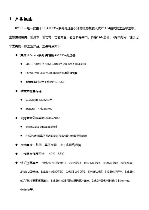
1.产品概述IPC335x是一款基于TI AM335x系列处理器设计的低功耗嵌入式PC104结构的工业级主板。
主板集成度高、低成本、低功耗、功能齐全,包含多路串口、多路CAN总线、2路千兆网,性价比非常高的一款工业产品。
主要特点如下:◆集成TI Sitara系列高性能AM335x处理器●500—720MHz ARM Cortex™-A8 32bit RISC内核●POWERVR SGX™530 3D图形加速处理引擎●可编程实时单元子系统PRU-ICSS◆板载大容量存储●512MByte DDR2内存●4GByte 工业级eMMC◆支持最大分辨率为2048x2048●支持RGB565/RGB888标准●在60Hz刷新率下可达1366x768的高分辨率显示输出◆直接集成千兆网,真正实现工业千兆网络通信◆工作温度范围可达:-40℃~85℃◆外扩资源丰富:包括2xCAN总线接口、2xSPI总线、1xGPMC总线、2xMMC总线、2xI2C总线、24bit LCD总线、8x12bit ADC/TSC 、1xUSB 2.0 OTG、5x4线UART、3x16bit PWM、3x32biteCAP脉冲宽度捕获输入、3x32bit eQEP正交编码脉冲输出、1xRGMII/RMII/GMII Ethernet、4xtimer等。
图1.1 IPC335x 工业级主板实物图MMC/GPMC x8bitEMIF 16-bitUART02x CAN BUS Ver. 2 A&B1x 24bit LCD interface8x 12-bit ADC5x UART 2x MMC/SD1x USB 2.0 OTG 2x McSPI 2x I2C1x JTAG 1x GPMC all1x Ethernet GMIIAM335XPC104 CONNECTOREMMC/NANDDDR2PMU1.1V 1.8V3.3VI2CDDR2 x2USBEthernet20-pin CONNECTORRS2321x McASPUSB0EMAC0图1.2 IPC335x 系统框架结构图2. 产品规格2.1硬件规格处理器TI AM335xUp to 720MHz ARM Cortex ™-A8 32bit RISC 内核 NEON™ SIMD 协处理器系列Power VR SGX™530 3D图形加速处理引擎(1)RAM 128MByte/256MByte/512MByte DDR2Flash 4~32GByte eMMC或4Gbit NAND FlashLED 1x 供电指示灯2x 可编程指示灯EEPROM 1x 256Kbit I2C EEPROMPower接口5V DCPC104接口及扩展接口资源(2)1x GPMC1x LCD Control 24bit接口8x 12-bit ADC input (与电阻屏引脚有复用情况)5x 4线UART(RX、TX、CTS、RTS)1x USB2.0 OTG2x McSPI2x MMC/SD/SDIO总线2x I2C2x DCAN1x RGMII/RMII/GMII2x PRU MII(3)1x PRU UART(3)1x MDIO4xtimer3x 32-bit eCAP3x 16-bit eHRPWM2x 32-bit eQPEJTAGSYS RESET_INSYS RESET_OUTAM335X EXT WAKEUP板上其他接口资源1x USB 2.0 OTG (MINI USB-AB) 1x Gigabit Ethernet RJ451x RS232 DB9(RX, TX)1xSYS_RESETn 按钮(1) 仅限于带有图形加速的版本(AM3354,AM3358,AM3359)。
OK335核心板的使用OK335x系列产品共分为三款核心板,分别是FET335xD,FET335xS,FET335xS-II。
三款产品的详细介绍及不同点请参考《OK335x产品规格书》,本文档重点讲述用户在使用核心板时的注意事项,请读者结合配套板卡的《硬件用户手册》,底板原理图,进行阅读分析。
FET335xD V2.1核心板注意事项注:FET335xD使用双排针孔连接器与底板相连,核心板共引出200Pin。
1核心板已经使用CPU的GPMC外部总线相关引脚,下面列表中的引脚连接到了NandFlash,用户使用核心板时务必注意。
这些引脚不可以重新定义其他的功能,否则会影响到系统的稳定性,核心板引出下面的引脚主要考虑到使用外部总线挂载外设功能,与NandFlash 分时复用。
核心板连接器ID核心板引脚ID CPU引脚ID引脚命名J2Pin73U7GPMC_D0J2Pin71V7GPMC_D1J2Pin69R8GPMC_D2J2Pin67T8GPMC_D3J2Pin65U8GPMC_D4J2Pin63V8GPMC_D5J2Pin61R9GPMC_D6J2Pin59T9GPMC_D7××V6GPMC_CSn0J2Pin30T17GPMC_WAIT0J2Pin87T7GPMC_OEn_REnJ2Pin83T6GPMC_BEn0_CLEJ2Pin85R7GPMC_ADVn_ALEJ2Pin89U6GPMC_WEnJ2Pin34U17GPMC_WPn注:X代表核心板未引出该引脚,NandFlash共使用CPU的15个引脚,其中14个引脚引出核心板。
2加密芯片,电源管理核心板连接器ID核心板引脚ID CPU引脚ID引脚命名J1Pin52C16I2C0_SCLJ1Pin50C17I2C0_SDA注:加密芯片和电源管理IC使用了I2C0,且把I2C0引出到底板,用户可以继续使用I2C0,请不要重新定这两个引脚为其他复用功能。
MYC-C335X-GW 硬件数据手册版本V1.0米尔电子|*********************版本记录版本号说明时间V1.0初始版本2020.1.10米尔电子产品命名规则简介核心板以”MYC”前缀,底板以“MYB”前缀,套件以”MYD”前缀。
核心板与底板连接方式分为:1.插针型,用字母C表示2.邮票孔,用字母Y表示3.金手指,用字母J表示米尔电子|*********************目录第1章产品概述与订购 (4)1.1产品概述........................................................................................................................................41.2产品订购........................................................................................................................................61.3AM335x 处理器简介 (7)第2章硬件资源 (10)2.1核心板硬件资源 (10)第3章硬件设计 (12)3.1核心板板对板接口.....................................................................................................................123.2核心板供电.................................................................................................................................133.3DDR3/DDR3L .............................................................................................................................153.4Nand Flash /eMMC Flash .........................................................................................................153.5EEPROM .....................................................................................................................................173.6Clock ............................................................................................................................................173.7系统启动管脚SYSBOOT (18)第4章底板设计建议 (19)4.1最小系统设计..............................................................................................................................194.2电源及上电顺序..........................................................................................................................194.3启动设置......................................................................................................................................204.4MYD-C335X-GW 参考设计.......................................................................................................204.5其它建议. (21)第5章电气参数 (22)5.1工作温度.....................................................................................................................................225.2GPIO 直流特性...........................................................................................................................225.3电源直流特性.. (22)第6章机械参数............................................................................................................................23附录一:免责声明..........................................................................................................................24附录二:联系我们..........................................................................................................................25附录三:技术支持说明 (27)米尔电子|*********************第1章产品概述与订购1.1产品概述米尔电子基于TI AM335x 处理器推出了核心板MYC-C335X-GW 及全套开发板MYD-C335X-GW 。
OK335X-Linux用户手册第一章OK335X简介OK335X开发板基于TI AM335X处理器,运行主频最高720M,支持Linux,WinCE,Android三大操作系统,可用于工业产品设计。
OK335X有核心板和底板组成,核心板主要芯片有:CPU,NandFlash,Memory,PowerManage。
使用我们的核心板,只需要根据您的业务需求开发自己的底板,这样可加速您的产品上市时间,让您从平台搭建的复杂环境中脱离。
下面我们具体描述OK335X核心板和底板资源。
OK335X产品图片如下所示:核心板硬件资源:1CPU主频:720M(支持AM3352,AM3354,AM3356,AM3357,AM3358,AM3359)2NandFlash:256M(Micro SLC)3Memory:265M(Micro DDR2)4PowerManage IC:TPS65217B(TI AM335X专用电源IC)底板资源:14路串口(2个232电平,2个TTL电平,232电平已经使用DB9座子引出,其中COM0作为调试串口使用,注意:OK335X-V1底板中UART4暂时不能使用,下一硬件版本将修正这个问题)。
21路100M网口3音频接口(1路Phone输出,1路Line-in输入)41个SD卡接口56个用户按键63路I2C接口71个LCD接口(支持RGB888模式,支持电阻触摸和电容触摸。
默认标配7寸电阻屏)81路PWM接口,用于蜂鸣器测试。
91路Can接口101路SDIO接口11多路用户IO接口12四路USB2.0接口,一路USB2.0OTG(目前板子为一路USB Host接口,后续会增加到四路USB HUB)131路SPI接口148路AD(其中4路用于电阻触摸,1路用于滑动变阻器AD测试,其余3路通过插针引出,另外滑动变阻器端有跳线设置,通过跳线可以设置这路AD用于插针引出,还是用于可调电阻测试)15引出总线接口(缺省未焊接底座)161个RESET按钮,用于系统复位。
Omap35xx介绍说明一、系统介绍 (2)1.系统资源简介 (2)二、omap35xx cpu板介绍说明 (3)1.omap35xx cpu板概况 (3)1.1 板卡主要资源 (3)1.2 板卡原理框图 (3)2.omap35xx cpu板扩展接口介绍 (4)3.内存映射 (6)4.启动设置说明 (7)三、omap35xx 大板介绍说明 (8)1.omap35xx 大板原理 (8)2、复位按键RK1、RK2、RK3 (8)3.按键接口介绍 (9)4.外接端口介绍 (9)4.1 USB端口介绍 (9)4.2 MMC/SD端口介绍 (10)4.3 语音端口介绍 (10)4.4 UART端口介绍 (11)4.5 LCD和触摸屏接口介绍 (11)4.6以太网接口介绍 (13)四、Linux系统开发 (14)1.开发环境搭建 (14)2.x-load编译 (14)2.u-boot编译 (16)3.内核编译 (16)4.文件系统建立 (17)5.MMC/SD卡挂载 (17)6.U盘挂载 (20)7.AUDIO测试 (21)8. 以太网测试 (21)9.TV OUT (22)10.演示程序介绍 (22)五、omap35xx烧写介绍 (25)1.u-boot烧写 (25)1.1 通过UART3烧写u-boot (25)1.2 更新u-boot (30)1.3 u-boot 启动模式设置 (33)2.内核烧写 (33)3.文件系统烧写 (34)六、TechV-35xx恢复到出厂设置 (35)一、系统介绍1.系统资源简介1.1 Omap35xx CPU 小板:CPU:Omap35xx(ARM:V7 Cortex-A8;DSP:TMS320C64x+™ 430-MHz) DDR:128MB;NANDFLASH:256MB;1.2 TechV-Omap35xx 大板:音频:1路输入,1路输出;视频:LCD输出,TV输出;8个输入按键;触摸屏输入;3.3V JTAG仿真接口;主从USB接口;SD/MMC卡接口;两个标准串口;标准RJ-45 10M/100M以太网接口;1.3 资料光盘;实验指导书;串口线(两根);交叉网线(一根);音频线(一根);二、omap35xx cpu板介绍说明1.omap35xx cpu板概况1.1 板卡主要资源存储器:64K内部SRAM;32位宽度DDR,容量为128MB;256MB的NAND FLASH;功能扩展:扩展了USB物理层接口,支持USB主、从工作模式;外扩语音模块,一路语音输入,一路语音输出;电源:独立的电源解决方案,外部只需要输入3.6—4.5V直流电。
IAC-335X-Kit Linux用户手册版本号v1.02013/03/19杭州启扬智能有限公司版权所有QIYANG TECHNOLOGY Co.,LtdCopyright Reserved修改历史记录版本号时间修订内容v1.02013-2-19创建有任何技术问题或需要帮助,请联系:***********************第1页共12页购买产品,请联系销售:********************更多信息请访问:目录前言 (3)一、IAC-335X-Kit资源简介 (4)1.1硬件资源 (4)1.2软件资源 (4)二、搭建嵌入式Linux开发环境 (5)三、启动和烧写Linux系统 (5)3.1启动方式 (5)3.2固化系统镜像到SD卡 (6)3.3烧写Linux系统到NAND Flash (6)四、编译u-boot和Linux内核 (6)4.1编译u-boot (6)4.2编译Linux内核 (7)五、应用程序的开发 (7)5.1Hello World (7)5.2交叉编译 (8)5.3运行应用程序 (8)5.4自动启动应用程序 (9)六、ubi文件系统制作 (9)七、IAC-335X-Kit的硬件接口测试 (10)有任何技术问题或需要帮助,请联系:***********************第2页共12页购买产品,请联系销售:********************更多信息请访问:前言欢迎使用杭州启扬智能科技有限公司产品IAC-335X-Kit,本产品Linux部分包含3份手册:IAC-335X-Kit Linux用户手册、IAC-335X-Kit硬件说明手册以及IAC-335X-Kit Linux测试手册。
硬件相关部分可以参考IAC-335X-Kit硬件说明手册,主板测试可以参考IAC-335X-Kit Linux测试手册。
使用之前请仔细阅读IAC-335X-Kit Linux用户手册以及IAC-335X-Kit硬件说明手册!公司简介杭州启扬智能科技有限公司位于美丽的西子湖畔,是一家集研发、生产、销售为一体的高新技术产业。
AM335X开发板产品板(IAC-335X-Kit)◆采用TI AM335X系列处理器,最高720MHz高速ARM Cortex-A8核心;◆准确定位工业控制领域,低功耗、低成本、高集成度核心模块+定制底板应用;◆提供管脚复用图表,客户可以精准匹配核心板管脚复用,实现更多应用;◆提供底板全部资源(含PCB文件)让您快速完成底板硬件设计,缩短研发周期;◆批量订购:可选 DDR2(max):512MB,Nandflash(max):64Gb,保证流畅的运行及存储空间;◆板载2路千兆网卡、多路RS232/485、2路CAN总线、GPMC总线等工业接口;◆核心板可全部升级工业级器件,高端B to B连接件,稳定适用于各种现场环境;◆预装可选Linux3.2、Android4.0.3操作系统,提供丰富例程及源代码;产品定位核心模块+定制接口底板应用!工业低功耗、低成本、高集成度;可提供完整的设计资料;可以根据需要委托定制;提供接口底板(PCB)源文件应用接口丰富的应用接口!2路10/100/1000M 以太网接口;5路RS232/RS485接口;2路 CAN 总线接口;LCD & VGA显示接口;......可扩展性灵活的总线可扩展性!GPMC总线接口;包含地址线、数据总线、片选;方便您扩展连接DSP、FPGA、扩展光网口、GPIO等等外设;高稳定性进口工业级B to B 连接器件!核心板与底板连接可靠、稳定;2 x 100 pin 0.8 间距;优异的电气性能及环境性能后续TI公司推出AM335X芯片的主频达1Ghz,该插件让稳定性更好......安赛卓尔科技优势:1、专业技术服务,同行难以跨越2、不断更新的软件资料,安卓系统、Linux系统、wince系统,后续免费提供资料3、专业的工业接口设计,充分扩展,是其他公司难以提供的4、超高性价比、优秀的解决方案5、与国内多家公司和厂家建立战略合作伙伴关系选择安赛卓尔,选择一个合作伙伴AM335X的优点有如下几个:第一:该器件是最实惠的Cortex-A8 处理芯片,这个对中国市场至关重要,甚至是决定性的因素。