nrf51822学习笔记之TIMER
- 格式:docx
- 大小:347.69 KB
- 文档页数:6
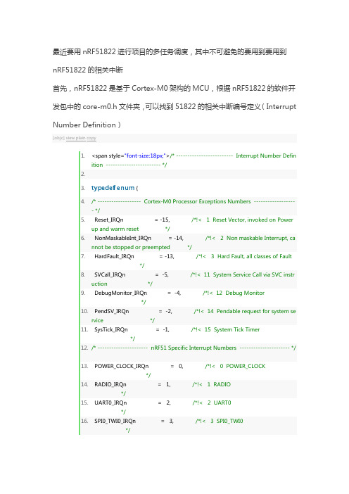
最近要用nRF51822进行项目的多任务调度,其中不可避免的要用到要用到nRF51822的相关中断首先,nRF51822是基于Cortex-M0架构的MCU,根据nRF51822的软件开发包中的core-m0.h文件夹,可以找到51822的相关中断编号定义(Interrupt Number Definition)[objc]view plain copy1.<span style="font-size:18px;">/* ------------------------- Interrupt Number Definition ------------------------ */2.3.typedef enum {4./* ------------------- Cortex-M0 Processor Exceptions Numbers ------------------- */5. Reset_IRQn = -15, /*!< 1 Reset Vector, invoked on Powerup and warm reset */6. NonMaskableInt_IRQn = -14, /*!< 2 Non maskable Interrupt, cannot be stopped or preempted */7. HardFault_IRQn = -13, /*!< 3 Hard Fault, all classes of Fault*/8. SVCall_IRQn = -5, /*!< 11 System Service Call via SVC instruction */9. DebugMonitor_IRQn = -4, /*!< 12 Debug Monitor*/10. PendSV_IRQn = -2, /*!< 14 Pendable request for system service */11. SysTick_IRQn = -1, /*!< 15 System Tick Timer*/12./* ---------------------- nRF51 Specific Interrupt Numbers ---------------------- */13. POWER_CLOCK_IRQn = 0, /*!< 0 POWER_CLOCK*/14. RADIO_IRQn = 1, /*!< 1 RADIO*/15. UART0_IRQn = 2, /*!< 2 UART0*/16. SPI0_TWI0_IRQn = 3, /*!< 3 SPI0_TWI0*/17. SPI1_TWI1_IRQn = 4, /*!< 4 SPI1_TWI1*/18. GPIOTE_IRQn = 6, /*!< 6 GPIOTE*/19. ADC_IRQn = 7, /*!< 7 ADC*/20. TIMER0_IRQn = 8, /*!< 8 TIMER0*/21. TIMER1_IRQn = 9, /*!< 9 TIMER1*/22. TIMER2_IRQn = 10, /*!< 10 TIMER2*/23. RTC0_IRQn = 11, /*!< 11 RTC0*/24. TEMP_IRQn = 12, /*!< 12 TEMP*/25. RNG_IRQn = 13, /*!< 13 RNG*/26. ECB_IRQn = 14, /*!< 14 ECB*/27. CCM_AAR_IRQn = 15, /*!< 15 CCM_AAR*/28. WDT_IRQn = 16, /*!< 16 WDT*/29. RTC1_IRQn = 17, /*!< 17 RTC1*/30. QDEC_IRQn = 18, /*!< 18 QDEC*/31. LPCOMP_COMP_IRQn = 19, /*!< 19 LPCOMP_COMP*/32. SWI0_IRQn = 20, /*!< 20 SWI0*/33. SWI1_IRQn = 21, /*!< 21 SWI1*/34. SWI2_IRQn = 22, /*!< 22 SWI2*/35. SWI3_IRQn = 23, /*!< 23 SWI3*/36. SWI4_IRQn = 24, /*!< 24 SWI4*/37. SWI5_IRQn = 25 /*!< 25 SWI5*/38.} IRQn_Type;39.</span>在进行中断处理时,一般都要按照这个步骤:1、对要用到的中断初始化;2、对用到的中断进行使能;3、对中断进行优先级设置1、中断初始化nRF51822的外部I/O(暂时理解的程度以及用过的中断只有I/O中断,其他中断没有实践过)中断是基于任务和事件模式的。
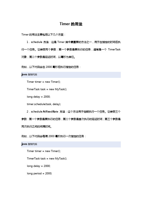
Timer的用法Timer的用法主要包括以下几个方面:1.schedule方法:这是Timer类中最重要的方法之一,用于在指定的时间后执行一个任务。
它接受两个参数:第一个参数是要执行的任务,通常是一个TimerTask 对象;第二个参数是延迟时间,以毫秒为单位。
例如,以下代码会在2000毫秒后执行指定的任务:java复制代码Timer timer = new Timer();TimerTask task = new MyTask();long delay = 2000;timer.schedule(task, delay);2.scheduleAtFixedRate方法:这个方法用于定期执行一个任务。
它接受三个参数:第一个参数是要执行的任务;第二个参数是首次执行的延迟时间;第三个参数是两次执行之间的间隔时间。
例如,以下代码会每隔2000毫秒执行一次指定的任务:java复制代码Timer timer = new Timer();TimerTask task = new MyTask();long delay = 2000;long period = 2000;timer.scheduleAtFixedRate(task, delay, period);3.cancel方法:这个方法用于取消所有已安排的任务。
调用这个方法后,所有已安排的任务将不再执行。
例如,以下代码将取消所有已安排的任务:java复制代码timer.cancel();以上就是Timer的主要用法。
需要注意的是,Timer并不保证任务的执行顺序,如果需要按照特定顺序执行任务,应该使用ScheduledExecutorService等更高级的并发工具。


Timer原理详解概述Timer是一种用于在预定时间之后执行某个操作的机制。
它可以被应用于各种场景,如定时任务、调度任务、计时等。
在编程中,Timer通常是一个线程,它会根据设置的时间来触发执行相应的任务。
Timer的基本原理Timer的基本原理是通过线程和系统时钟来实现的。
当创建一个Timer时,它会创建一个新的线程,该线程会不断地检查是否有任务需要执行。
此外,Timer还会记录每个任务的触发时间,并根据系统时钟来判断是否到了任务触发的时间点。
Timer的工作流程Timer的工作流程可以概括为以下几个步骤: 1. 创建Timer对象,并设置任务的触发时间和执行操作。
2. Timer启动后,会创建一个新的线程用于检查任务的触发时间。
3. 每隔一段时间,线程会检查一次当前时间和任务触发时间是否匹配,并执行相应的操作。
4. 当任务触发时间到达后,执行相应的操作,并重置触发时间。
5. 重复步骤3和步骤4,直到Timer被取消或终止。
Timer的核心组件Timer的核心组件包括线程、计时器和任务队列。
线程线程是Timer的核心之一。
当Timer启动时,它会创建一个新的线程,用于执行任务队列的检查。
线程负责定期检查任务的触发时间,并根据触发时间来执行相应的操作。
计时器是Timer的另一个核心组件。
它负责记录每个任务的触发时间,并与系统时钟进行比较来确定是否需要执行任务。
任务队列任务队列是Timer用于存储待执行的任务的数据结构。
当任务的触发时间到达时,相应的任务会被取出并执行。
Timer中的任务队列通常使用优先级队列来实现,以确保任务按照预定的触发时间顺序执行。
Timer的调度策略Timer的调度策略决定了任务何时被执行。
Timer的调度策略通常有两种:绝对时间调度和相对时间调度。
绝对时间调度绝对时间调度是指根据任务的绝对触发时间来执行任务。
在Timer中,任务的触发时间是一个时间戳,当系统时钟达到该时间戳时,相应的任务被执行。

Timer寄存器说明1、定时器/计数器系统控制寄存器1(TSCR1)TSCR1 寄存器是定时器模块的总开关,它决定模块是否启动以及在中断等待、BDM 方式下的行为,还包括标志的管理方式。
其各位的意义如下:TEN:定时器使能位,此外它还控制定时器的时钟信号源。
要使用定时器模块的IC/OC 功能,必须将TEN 置位。
如果因为某种原因定时器没有使能,脉冲累加器也将得不到ECLK/64 时钟,因为ECLK/64 是由定时器的分频器产生的,这种情况下,脉冲累加器将不能进行引脚电平持续时间的累加。
0:定时器/计数器被禁止,有利于降低功耗。
1:定时器/计数器使能,正常工作。
TSWAI:等待模式下计时器关闭控制位。
【注意】定时器中断不能用于使MCU 退出等待模式。
0:在中断等待模式下允许MCU 继续运行。
1:当MCU 进入中断等待模式时,禁止计时器。
TSFRZ:在冻结模式下计时器和计数器停止位。
0:在冻结模式下允许计时器和计数器继续运行。
1:在冻结模式下禁止计时器和计数器,用于仿真调试。
【注意】TSFRZ 不能停止脉冲累加。
TFFCA:定时器标志快速清除选择位。
0:定时器标志普通清除方式。
1:对于TFLGl($0E)中的各位,读输入捕捉寄存器或者写输出比较寄存器会自动清除相应的标志位CnF。
对于TFLG2($0F)中的各位,任何对TCNT 寄存器($04、$05)的访问均会清除TOF 标志;任何对PACN3 和PACN2 寄存器($22,$23)的访问都会清除PAFLG 寄存器($21)中的PAOVF 和PAIF 位。
任何对PACN1 和PACN0 寄存器($24,$25)的访问都会清除PBFLG 寄存器($21)中的PBOVF 位。
【说明】这种方式的好处是削减了另外清除标志位的软件开销。
此外,必须特别注意避免对标志位的意外清除。
2、计时器系统控制寄存器2(TSCR2)寄存器偏移量:$000DTOI:定时器/计时器溢出中断使能。
nrf51822数据⼿册_引脚图_参数Copyright ? 2014 Nordic Semiconductor ASA. All rights reserved.Reproduction in whole or in part is prohibited without the prior written permission of the copyright holder.nRF51822Multiprotocol Bluetooth ? low energy/2.4 GHz RF System on Chip Product Specification v3.3Key Features2.4 GHz transceiver-93 dBm sensitivity in Bluetooth low energy mode250 kbps, 1 Mbps, 2 Mbps supported data ratesTX Power -20 to +4 dBm in 4 dB stepsTX Power -30 dBm Whisper mode13 mA peak RX, 10.5 mA peak TX (0 dBm)9.7 mA peak RX, 8 mA peak TX (0 dBm) with DC/DCRSSI (1 dB resolution)ARM Cortex-M0 32 bit processor275 µA/MHz running from flash memory150 µA/MHz running from RAMSerial Wire Debug (SWD)S100 series SoftDevice readyMemory256 kB or 128 kB embedded flash program memory16 kB or 32 kB RAMOn-air compatibility with nRF24L seriesFlexible Power ManagementSupply voltage range 1.8 V to 3.6 V4.2 µs wake-up using 16 MHz RCOSC0.6 µA at 3 V OFF mode1.2 µA at 3 V in OFF mode + 1 region RAM retention2.6 µA at 3 V ON mode, all blocks IDLE8/9/10 bit ADC - 8 configurable channels31 General Purpose I/O PinsOne 32 bit and two 16 bit timers with counter modeSPI Master/SlaveLow power comparatorTemperature sensorTwo-wire Master (I2C compatible)UART (CTS/RTS)CPU independent Programmable Peripheral Interconnect (PPI)Quadrature Decoder (QDEC)AES HW encryptionReal Timer Counter (RTC)Package variantsQFN48 package, 6 x 6 mmWLCSP package, 3.50 x 3.83 x 0.50 mmWLCSP package, 3.50 x 3.83 x 0.35 mmWLCSP package, 3.83 x 3.83 x 0.50 mmWLCSP package, 3.83 x 3.83 x 0.35 mmWLCSP package, 3.50 x 3.33 x 0.50 mm Applications Computer peripherals and I/O devices Mouse Keyboard Multi-touch trackpad ?Interactive entertainment devices ?Remote control ?Gaming controller ?Beacons ?Personal Area Networks Health/fitness sensor and monitor devices Medical devices Key-fobs + wrist watches Remote control toysLiability disclaimerNordic Semiconductor ASA reserves the right to make changes without further notice to the product to improve reliability, function or design. Nordic Semiconductor ASA does not assume any liability arising out of the application or use of any product or circuits described herein.Life support applicationsNordic Semiconductor’s products are not designed for use in life support appliances, devices, or systems where malfunction of these products can reasonably be expected to result in personal injury. Nordic Semiconductor ASA customers using or selling these products for use in such applications do so at their own risk and agree to fully indemnify Nordic Semiconductor ASA for any damages resulting from such improper use or sale.Contact detailsFor your nearest distributor, please visit .Information regarding product updates, downloads, and technical support can be accessed through your My Page account on our home page.RoHS and REACH statementNordic Semiconductor's products meet the requirements of Directive 2002/95/EC of the EuropeanParliament and of the Council on the Restriction of Hazardous Substances (RoHS) and the requirements of the REACH regulation (EC 1907/2006) on Registration, Evaluation, Authorization and Restriction of Chemicals. The SVHC (Substances of Very High Concern) candidate list is continually being updated.Complete hazardous substance reports, material composition reports and latest version of Nordic's REACH statement can be found on our website .Main office:Phone: +47 72 89 89 00Fax: +47 72 89 89 89 Otto Nielsens veg 127052 Trondheim NorwayMailing address:Nordic Semiconductor P .O. Box 23367004 TrondheimNorwayDatasheet StatusRevision History StatusDescription Objective Product Specification (OPS)This product specification contains target specifications for product development.Preliminary Product Specification (PPS)This product specification contains preliminary data; supplementary datamay be published from Nordic Semiconductor ASA later.Product Specification (PS)This product specification contains final product specifications. NordicSemiconductor ASA reserves the right to make changes at any timewithout notice in order to improve design and supply the best possibleproduct.DateVersion Description July 2016 3.3Added documentation for the nRF51822 CTAA version of the chip.Added content:Section 9.5 “CTAA WLCSP package” on page 71Section 11.9 “CTAA WLCSP package” on page 118Updated content:Feature list on the front page.Section 2.2.3 “CEAA, CFAC, CTAA, and CTAC WLCSP ball assignment and functions”on page 17Section 3.2.1 “Code organization” on page 22Section 3.2.2 “RAM organization” on page 22Section 3.3 “Memory Protection Unit (MPU)” on page 23Section 7.1.2 “CTAA and CTAC light sensitivity” on page 39Section 7.2 “CTAA and CTAC mechanical strength” on page 39Section 10.6 “Code ranges and values” on page 76Section 10.7 “Product options” on page 78Chapter 11 “Reference circuitry” on page 79. Added resistor R1 on the schematicsfor all variants.January 2016 3.2Added documentation for the nRF51822 CTAC version of the chip.Added content:Section 4.10.1 “Enable 4 Mbps SPIS bit rate” on page35Section 7.2 “CTAA and CTAC mechanical strength” on page39Section 9.6 “CTAC WLCSP package” on page72Section 11.10 “CTAC WLCSP package” on page124Updated content:Feature list on the front page.Section 2.2.3 “CEAA, CFAC, CTAA, and CTAC WLCSP ball assignment and functions”on page17Section 3.2.1 “Code organization” on page22Section 3.2.2 “RAM organization” on page22Section 3.3 “Memory Protection Unit (MPU)” on page23Chapter 6 “Absolute maximum ratings” on page38Section 7.1 “WLCSP light sensitivity” on page39Section 8.1.2 “16 MHz crystal oscillator (16M XOSC)” on page41Section 8.1.5 “32.768 kHz crystal oscillator (32k XOSC)” on page43Section 8.1.6 “32.768 kHz RC oscillator (32k RCOSC)” on page44Section 8.2 “Power management” on page45Section 8.8 “Serial Peripheral Interface Slave (SPIS) specifications” on page57 Section 10.6 “Code ranges and values” on page76Section 10.7 “Product options” on page78October 2014 3.1Added documentation for the following versions of the chip:nRF51822-QFAC AA0nRF51822-QFAC Ax0nRF51822-CDAB AA0nRF51822-CDAB Ax0nRF51822-CFAC AA0nRF51822-CFAC Ax0(The x in the build codes can be any number between 0 and 9.)Added content:Section 2.2.2 “CDAB WLCSP ball assignment and functions” on page14Section 9.2 “CDAB WLCSP package” on page68Section 9.4 “CFAC WLCSP package” on page70Updated content:Feature list on the front page.Section 2.2.3 “CEAA and CFAC WLCSP ball assignment and functions” on page17 Section 3.2.1 “Code organization” on page22Section 3.2.2 “RAM organization” on page22Section 3.3 “Memory Protection Unit (MPU)” on page23Section 8.2 “Power management” on page45Section 8.3 “Block resource requirements” on page49Section 8.12 “Analog to Digital Converter (ADC) specifications” on page61Section 10.6 “Code ranges and values” on page76Section 10.7 “Product options” on page78August 2014 3.0Update to reflect the changes in build code:nRF51822-QFAA Hx0nRF51822-CEAA Ex0nRF51822-QFAB Cx0(The x in the build codes can be any number between 0 and 9.)If you are working with a previous revision of the chip, read version 2.x of the document. Added content:Section 8.5.3 “Radio current consumption with DC/DC enabled” on page51Section 11.1.1 “PCB layout example” on page80Updated content:Feature list on the front page.Section 2.1 “Block diagram” on page11Section 3.2.1 “Code organization” on page22Section 3.2.2 “RAM organization” on page22Section 3.3 “Memory Protection Unit (MPU)” on page23Section 3.4 “Power management (POWER)” on page24Section 3.6 “Clock management (CLOCK)” on page28Section 3.8 “Debugger support” on page31Section 4.2 “Timer/counters (TIMER)” on page33Chapter 5 “Instance table” on page37Chapter 7 “Operating conditions” on page39Section 8.1.2 “16 MHz crystal oscillator (16M XOSC)” on page41Section 8.1.3 “32 MHz crystal oscillator (32M XOSC)” on page42Section 8.1.4 “16 MHz RC oscillator (16M RCOSC)” on page43Section 8.1.6 “32.768 kHz RC oscillator (32k RCOSC)” on page44Section 8.1.7 “32.768 kHz Synthesized oscillator (32k SYNT)” on page44Section 8.2 “Power management” on page45Section 8.3 “Block resource requirements” on page49Section 8.4 “CPU” on page49Section 8.5.6 “Radio timing parameters” on page55Section 8.5.7 “Antenna matching network requirements” on page55Section 8.7 “Universal Asynchronous Receiver/Transmitter (UART) specifications”on page56Section 8.8 “Serial Peripheral Interface Slave (SPIS) specifications” on page57Section 8.12 “Analog to Digital Converter (ADC) specifications” on page61Section 8.13 “Timer (TIMER) specifications” on page62Section 8.15 “Temperature sensor (TEMP)” on page62Section 8.22 “Non-Volatile Memory Controller (NVMC) specifications” on page65Section 8.24 “Low Power Comparator (LPCOMP) specifications” on page66Section 9.2 “CDAB WLCSP package” on page68Section 10.7.2 “Development tools” on page78Chapter 11 “Reference circuitry” on page79October 2013 2.0This version of the document will target the nRF51822 QFAA G0 revision of the chip. If you are working with a previous revision of the chip, read version 1.3 or earlier of thedocument.Updated the following sections:Key Feature list on the front page,Chapter 1 “Introduction” on page10,Section 2.1 “Block diagram” on page11,Section 2.2 “Pin assignments and functions” on page12,Section 3.2 “Memory” on page21,Section 3.5 “Programmable Peripheral Interconnect (PPI)” on page27,Section 3.7 “GPIO” on page31,Section 4.1 “2.4 GHz radio (RADIO)” on page32,Section 4.2 “Timer/counters (TIMER)” on page33,Section 4.3 “Real Time Counter (RTC)” on page33,Section 4.10 “Serial Peripheral Interface (SPI/SPIS)” on page35,Section 4.12 “Universal Asynchronous Receiver/Transmitter (UART)” on page36,Section 4.14 “Analog to Digital Converter (ADC)” on page36,Section 4.15 “GPIO Task Event blocks (GPIOTE)” on page36,Chapter 5 “Instance table” on page37,Chapter 6 “Absolute maximum ratings” on page38,Chapter 8 “Electrical specifications” on page40,Section 8.1 “Clock sources” on page40,Section 8.1.2 “16 MHz crystal oscillator (16M XOSC)” on page41,Section 8.1.3 “32 MHz crystal oscillator (32M XOSC)” on page42,Section 8.2 “Power management” on page45,Section 8.3 “Block resource requirements” on page49,Section 8.7 “Universal Asynchronous Receiver/Transmitter (UART) specifications” on page56,Section 8.9 “Serial Peripheral Interface (SPI) Master specifications” on page58,Section 8.11 “GPIO Tasks and Events (GPIOTE) specifications” on page60,Section 8.13 “Timer (TIMER) specifications” on page62,Section 8.16 “Random Number Generator (RNG) specifications” on page63,Section 8.17 “AES Electronic Codebook Mode Encryption (ECB) specifications” on page63, Section 8.18 “AES CCM Mode Encryption (CCM) specifications” on page63,Section 8.19 “Accelerated Address Resolver (AAR) specifications” on page63,Section 8.21 “Quadrature Decoder (QDEC) specifications” on page64,Section 11.1 “PCB guidelines” on page79,Section 11.3 “QFAA QFN48 package” on page82, andSection 11.7 “CEAA WLCSP package” on page106.Added the following sections:Section 3.3 “Memory Protection Unit (MPU)” on page23,Section 4.5 “AES CCM Mode Encryption (CCM)” on page34,Section 4.6 “Accelerated Address Resolver (AAR)” on page34,Section 4.16 “Low Power Comparator (LPCOMP)” on page36,Section 8.5.7 “Antenna matching network requirements” on page55,Section 8.8 “Serial Peripheral Interface Slave (SPIS) specifications” on page57,Section 8.18 “AES CCM Mode Encryption (CCM) specifications” on page63,Section 8.19 “Accelerated Address Resolver (AAR) specifications” on page63, and Section 8.24 “Low Power Comparator (LPCOMP) specifications” on page66.May 2013 1.3Updated schematics and BOMs in section 11.3 on page 61.April 2013 1.2Added chip variant nRF51822-CEAA. Updated feature list on front page. UpdatedSection 3.2.1 on page 15, Section 3.2.2 on page 15, Chapter 6 on page 28,Section 10.4 on page 52, and Section 10.5.1 on page 53.AddedSection 2.2.2 on page 10, Section 7.1 on page 29, Section 9.2 on page 50,and Section 11.3 on page 61.Removed PCB layouts in Chapter 11 on page 54.March 2013 1.1Added chip variant nRF51822-QFAB. Added 32 MHz crystal oscillator feature. Updated feature list on front page. Moved subsection ‘Calculating current when the DC/DCconverter is enabled’ from chapter 8 to the nRF51 Series Reference Manual.UpdatedChapter 1 on page 6, Section 2.2 on page 8, Section 3.2 on page 12,Section 3.5 on page 16, Section 3.5.1 on page 17, Section 4.2 on page 21, Chapter 5 onpage 24, Section 8.1 on page 27, Section 8.1.2 on page 28, Section 8.1.5 on page 30,Section 8.2 on page 32, Section 8.3 on page 34, Section 8.5.3 on page 36, Section 8.8 onpage 40, Section 8.9 on page 41, Section 8.10 on page 42, Section 8.14 on page 43,Chapter 10 on page 47, Section 11.2 on page 51, Section 11.3 on page 54, andSection 11.4 on page 57.AddedSection 3.5.4 on page 19, Section 8.1.3 on page 29, andSection 11.1 on page 50.November 2012 1.0Changed from PPS to PS. Updated the feature list on the front page.UpdatedTable 11 on page 25, Table 12 on page 26, Table 14 on page 28,Table 15 on page 28, Table 16 on page 29, Table 17 on page 29,Table 18 on page 30, Table 19 on page 31, Table 21 on page 32,Table 22 on page 32, Table 23 on page 33,Table 27 on page 36,Table 28 on page 37, Table 29 on page 37, Table 31 on page 38,Table 32 on page 38, Table 35 on page 39, Table 38 on page 40,Table 39 on page 40, Table 55 on page 47, Figure 9 on page 48, andTable 57 on page 50.Table of contents1Introduction (10)1.1Required reading (10)1.2Writing conventions (10)2Product overview (11)2.1Block diagram (11)2.2Pin assignments and functions (12)3System blocks (20)3.1CPU (20)3.2Memory (21)3.3Memory Protection Unit (MPU) (23)3.4Power management (POWER) (24)3.5Programmable Peripheral Interconnect (PPI) (27)3.6Clock management (CLOCK) (28)3.7GPIO (31)3.8Debugger support (31)4Peripheral blocks (32)4.1 2.4 GHz radio (RADIO) (32)4.2Timer/counters (TIMER) (33)4.3Real Time Counter (RTC) (33)4.4AES Electronic Codebook Mode Encryption (ECB) (33)4.5AES CCM Mode Encryption (CCM) (34)4.6Accelerated Address Resolver (AAR) (34)4.7Random Number Generator (RNG) (34)4.8Watchdog Timer (WDT) (34)4.9Temperature sensor (TEMP) (35)4.10Serial Peripheral Interface (SPI/SPIS) (35)4.11Two-wire interface (TWI) (35)4.12Universal Asynchronous Receiver/Transmitter (UART) (36)4.13Quadrature Decoder (QDEC) (36)4.14Analog to Digital Converter (ADC) (36)4.15GPIO Task Event blocks (GPIOTE) (36)4.16Low Power Comparator (LPCOMP) (36)5Instance table (37)6Absolute maximum ratings (38)7Operating conditions (39)7.1WLCSP light sensitivity (39)7.2CTAA and CTAC mechanical strength (39)8Electrical specifications (40)8.1Clock sources (40)8.2Power management (45)8.3Block resource requirements (49)8.4CPU (49)8.5Radio transceiver (50)8.6Received Signal Strength Indicator (RSSI) specifications (55)8.7Universal Asynchronous Receiver/Transmitter (UART) specifications (56)8.8Serial Peripheral Interface Slave (SPIS) specifications (57)8.9Serial Peripheral Interface (SPI) Master specifications (58)8.10I2C compatible Two Wire Interface (TWI) specifications (59)8.11GPIO Tasks and Events (GPIOTE) specifications (60)8.12Analog to Digital Converter (ADC) specifications (61)8.13Timer (TIMER) specifications (62)8.14Real Time Counter (RTC) (62)8.15Temperature sensor (TEMP) (62)8.16Random Number Generator (RNG) specifications (63)8.17AES Electronic Codebook Mode Encryption (ECB) specifications (63) 8.18AES CCM Mode Encryption (CCM) specifications (63)8.19Accelerated Address Resolver (AAR) specifications (63)8.20Watchdog Timer (WDT) specifications (64)8.21Quadrature Decoder (QDEC) specifications (64)8.22Non-Volatile Memory Controller (NVMC) specifications (65)8.23General Purpose I/O (GPIO) specifications (66)8.24Low Power Comparator (LPCOMP) specifications (66)9Mechanical specifications (67)9.1QFN48 package (67)9.2CDAB WLCSP package (68)9.3CEAA WLCSP package (69)9.4CFAC WLCSP package (70)9.5CTAA WLCSP package (71)9.6CTAC WLCSP package (72)10Ordering information (73)10.1Chip marking (73)10.2Inner box label (73)10.3Outer box label (74)10.4Order code (74)10.5Abbreviations (75)10.6Code ranges and values (76)10.7Product options (78)11Reference circuitry (79)11.1PCB guidelines (79)11.2Reference design schematics (81)11.3QFAA QFN48 package (82)11.4QFAB QFN48 package (88)11.5QFAC QFN48 package (94)11.6CDAB WLCSP package (100)11.7CEAA WLCSP package (106)11.8CFAC WLCSP package (112)11.9CTAA WLCSP package (118)11.10CTAC WLCSP package (124)12Glossary (130)万联芯城专注电⼦元器件配单服务,只售原装现货库存,万联芯城电⼦元器件全国供应,专为终端⽣产,研发企业提供现货物料,价格优势明显,BOM配单整单采购可享优惠价,提交BOM表报价,最快可当天发货,电⼦元器件现货销售,满⾜客户物料需求,万联芯城凭借丰富的电⼦元器件供应链体系已在业内打下良好的品牌⼝碑,完整PDF资料点击进⼊万联芯城。
Peripheral interface外设接口所有外设可通过AHB和APB总线寄存器被访问,就如同通过task, event, interrupt寄存器进行访问一样.1、外设ID:每个外设都分配了0X1000 bytes 的空间,也就是说每个外设在APB总线上一共有1024个4 bytes的寄存器(0X1000=4096),第一个外设的基地址是0x4000 0000, ID号为0. 基地址为0x4000 1000的外设ID号为1,依次类推基地址为0x4001 F000的外设ID号为31.2、TASK :作用:用来触发外设的动作(actions),例如开始某个特定的行为。
外设都能实现不同的Task,每个Task在该外设任务寄存器组(peripheral’s task register group) 中都有一个单独的寄存器触发条件:可以通过软件写“1”到任务寄存器(task register)或者由外设本身或其他外设触发相应的任务信号来触发某个TASK3、Event:作用:用来通知外设或CPU某个事件发生了,例如某个外设的状态改变了。
一个外设能够产生多个Event,每个Event在事件寄存器组(peripheral’s event register group)中都有一个单独的寄存器。
产生条件: 外设本身触发了某个事件信号(event signal),于是事件寄存器(event register)会更新用以反映该事件的发生。
事件寄存器只有在软件向其写0的时候,才会被清零。
4、Shortcuts:链接同一个外设的事件(event)和任务(task)的快捷方式,当事件发生的时候可以通过Shortcuts直接触发任务。
与PPI的功能类似,但是传播时间比PPI更短。
快捷方式是被预先定义了的,用户不可以通过软件配置,用户只能对其进行使能和关闭。
一个快捷方式占1位,每个外设最多32个快捷方式。
5、Interrupts:中断由事件(event)产生,可以打断CPU程序流。
大量的TIMER task/event及中断,可以使各种系统外设(包括GPIO)通过PPI 系统执行定时或记数任务(timing/count tasks).PPI系统也可以使能定时器(TIMER task/event features)来产生周期性输出(periodic output)或PWM信号到任意的GPIO口。
The PPI system also enables the TIMER task/event features to generate periodic output and PWM signals to any GPIO.定时计数器的时钟源是HFCLK,并可以通过一个4 bit (1/2X) 分配器对HFCLK进行分频.TIMER可以处于两种模式:1定时模式(Timer mode)2计数模式(Counter mode)两种模式都可以通过触发启动或停止任务(START task or STOP task)来启动或停止TIMER。
TIMER是count-up timer:Timer mode:每个定时器周期(F TIMER),内部计数寄存器(Counter register )+1. Counter mode:每次COUNT task被触发的时候,Counter register +1. 此模式下,FTIMER和分频系数就不起作用了。
TIMER可以通过位宽寄存器(BITMODE register)设置计数最大值(maximum value).分频和位宽寄存器(PRESCALER register and the BITMODE register)只能在TIMER停止运行的时候对其进行修改,否则结果难以预料。
当计数超过了最大值时,计数寄存器会溢出,并自动从0重新开始计数。
可通过执行CLEAR task 使TIMER清0。
比较和捕获(Compare/Capture):比较:每个捕获比较寄存器(CC[0..3])都可以产生一个COMPARE event.当某个计数值计到与capture compare register CC[n]中的值相等时,就会产生一个COMPARE[n] event,这两个n 是对应着的。
捕获:每个capture/compare register都可以执行一个capture task。
每次capture[n] task被触发,计数值都会被复制到CCP[n]寄存器every time the CAPTURE[n] task is triggered the Counter value is copied to the CC[n] register.任务的优先权(Task priority):当START task and the STOP task同时来到的时候,STOP task优先任务延时(Task delays):CLEAR task, COUNT task and the STOP task 都会在一个HFCLK时钟周期内完成,子电源模式下,START task 需要更长的时间。
The CLEAR task, COUNT task and the STOP task will guarantee to take effect within one clock cycle of the HFCLK. Depending on sub-power mode, the START task may require longer time to take effect。
示例代码:static void timer2_init(void){NRF_CLOCK->EVENTS_HFCLKSTARTED = 0; //16MHZNRF_CLOCK->TASKS_HFCLKSTART = 1;while (NRF_CLOCK->EVENTS_HFCLKSTARTED == 0) {} //wait for clk startNRF_TIMER2->MODE = TIMER_MODE_MODE_Timer; //Mode :TimerNRF_TIMER2->PRESCALER = 4; // 16M/2^4=1usNRF_TIMER2->CC[0] = LED_INTENSITY_LOW; //32NRF_TIMER2->CC[1] = (LED_INTENSITY_HALF*2); //128*2=256 us =0.256ms (1~224)NRF_TIMER2->CC[2] = LED_INTENSITY_HIGH; //224NRF_TIMER2->INTENSET=TIMER_INTENSET_COMPARE2_Enabled<< TIMER_INTENSET_COMPARE2_Pos;//1<<16 enable Interrupt 使能中断NRF_TIMER2->SHORTS =(TIMER_SHORTS_COMPARE1_CLEAR_Enabled << TIMER_SHORTS_COMPARE1_CLEAR_Pos);//clear compare1 event}✧#define NRF_TIMER2 ((NRF_TIMER_Type*) NRF_TIMER2_BASE)其中:●#define NRF_TIMER2_BASE 0x4000A000ULtypedef struct { //TIMER Structure__O uint32_t TASKS_START; // Start Timer.__O uint32_t TASKS_STOP; //Stop Timer.__O uint32_t TASKS_COUNT; //Increment Timer (In counter mode).__O uint32_t TASKS_CLEAR; // Clear timer.__O uint32_t TASKS_SHUTDOWN; //Shutdown timer.__I uint32_t RESERVED0[11];__O uint32_t TASKS_CAPTURE[4]; // Capture Timer value to CC[n] registers.__I uint32_t RESERVED1[60];__IO uint32_t EVENTS_COMPARE[4]; // Compare event on CC[n] match.__I uint32_t RESERVED2[44];__IO uint32_t SHORTS; // Shortcuts for Timer.__I uint32_t RESERVED3[64];__IO uint32_t INTENSET; // Interrupt enable set register.__IO uint32_t INTENCLR; //Interrupt enable clear register.__I uint32_t RESERVED4[126];__IO uint32_t MODE; // Timer Mode selection.__IO uint32_t BITMODE; //Sets timer behaviour.__I uint32_t RESERVED5;__IO uint32_t PRESCALER; // 4-bit prescaler to source clock frequency (max value 9). Source . clock frequency is divided by 2^SCALE.__I uint32_t RESERVED6[11];__IO uint32_t CC[4]; //Capture/compare registers.__I uint32_t RESERVED7[683];__IO uint32_t POWER; // Peripheral power control.} NRF_TIMER_Type;NRF_TIMER2->MODE = TIMER_MODE_MODE_Timer; //Mode :Timer 0NRF_TIMER2->PRESCALER = 4;// 16M/2^4=1usNRF_TIMER2->CC[0] = 32NRF_TIMER2->INTENSET = 1<<16//TIMER_INTENSET_COMPARE2_Enabled << TIMER_INTENSET_COMPARE2_Pos;使能中断NRF_TIMER2->SHORTS = 1<<1//(TIMER_SHORTS_COMPARE1_CLEAR_Enabled << TIMER_SHORTS_COMPARE1_CLEAR_Pos); //clear compare1 eventvoid TIMER2_IRQHandler(void){if ((NRF_TIMER2->EVENTS_COMPARE[2] == 1) &&(NRF_TIMER2->INTENSET & TIMER_INTENSET_COMPARE2_Msk)) // Clear interrupt.NRF_TIMER2->EVENTS_COMPARE[2] = 0;…..}主函数:NVIC_EnableIRQ(TIMER2_IRQn); // Enable interrupt on Timer__enable_irq();NRF_TIMER2->TASKS_START = 1; // Start the timer.。