Circuit Modeling of Carbon Nanotube Interconnects and their Performance Estimation
- 格式:pdf
- 大小:172.27 KB
- 文档页数:4

碳纳米管电梯的作文英文回答:Carbon nanotube (CNT) elevators are a theoretical means of vertical transportation that utilize the strength, flexibility, and electrical conductivity of carbon nanotubes (CNTs). CNTs are cylindrical structures made of carbon atoms arranged in a hexagonal lattice, and they possess remarkable mechanical and electrical propertiesthat make them promising materials for a wide range of applications, including energy storage, electronics, and transportation.The concept of CNT elevators was first proposed in 1999 by Richard Smalley and his colleagues at Rice University. They envisioned a system in which a series of CNT ropes would be suspended from a high-altitude platform, with a spacious cabin attached to the bottom of the ropes. The cabin would be powered by an electric motor, which would use the CNT ropes as electrical conductors to power theelevator up and down.CNT elevators offer several potential advantages over conventional elevators. First, CNTs are extremely strong and lightweight, so CNT ropes could be much longer and lighter than steel cables, allowing for the construction of elevators that are significantly taller than existing ones. Second, CNTs are good electrical conductors, so they could be used to power the elevator directly, eliminating the need for a separate power cable. Third, CNTs are flexible and elastic, so they could withstand high winds and earthquakes without breaking.However, there are also several challenges that must be overcome before CNT elevators can become a reality. First, CNTs are expensive to produce, so the cost of building a CNT elevator would be significantly higher than the cost of building a conventional elevator. Second, CNTs aresensitive to heat and moisture, so they would need to be protected from the elements in order to ensure their long-term durability. Third, CNTs can be damaged by electromagnetic fields, so they would need to be shieldedfrom sources of electromagnetic radiation.Despite these challenges, CNT elevators remain a promising concept with the potential to revolutionize vertical transportation. With continued research and development, it is possible that CNT elevators could one day become a reality, providing a safe, efficient, and environmentally friendly way to move people and goods up and down tall buildings.中文回答:碳纳米管电梯是一种理论上的垂直运输方式,它利用了碳纳米管(CNT)的强度、柔韧性和导电性。

The Physical Properties of CarbonNanotubesCarbon nanotubes (CNTs) are one of the most fascinating materials developed in the past few decades. They are cylindrical nanostructures composed of carbon atoms arranged in a hexagonal pattern. CNTs have unique properties, including high strength and stiffness, small size, exceptional electrical conductivity, and thermal conductivity. These properties make them preferable for numerous applications in several fields, including electronics, materials science, aerospace, and biotechnology.Structure of carbon nanotubesCarbon nanotubes have two primary structural types: single-walled nanotubes (SWNTs) and multi-walled nanotubes (MWNTs). SWNTs consist of a single rolled sheet, while MWNTs contain multiple rolled sheets. The diameter of SWNTs ranges from 0.4to 2 nm, while MWNTs have diameters ranging from 2 to 100 nm. The length of CNTs is usually several micrometers, but they can be longer.Thanks to their small dimensions and tubular structure, CNTs have a high aspect ratio, which means that their length is much greater than their diameter. This aspect ratio gives CNTs their unique mechanical properties. They are exceptionally strong and stiff, with a Young's modulus three to four times higher than that of steel. Moreover, CNTs are quite resilient, and their deformation before failure is much more elevated than conventional materials, making them perfect for use in new structural materials.Electrical properties of carbon nanotubesOne of the most remarkable properties of CNTs is their electrical conductivity. They have excellent electrical properties, which means they can conduct electricity even better than copper. SWNTs are metallic or semiconducting depending on their chiral angle, while MWNTs are usually metallic.SWNTs have particular band structures, and their electrical properties depend heavily on their atomic structure. The electronic properties of CNTs make them ideal for use in electronic applications, such as field-effect transistors, diodes, and sensors. CNTs have the potential to improve the performance of transistors and other electronic devices significantly.Thermal properties of carbon nanotubesCNTs also have exceptional thermal conductivity, making them useful in thermal management materials. The thermal conductivity of CNTs is approximately seven times higher than that of copper. Moreover, CNTs are excellent heat conductors at the nanoscale, which gives them the potential to improve the efficiency of thermal management materials in electronic devices.Other physical properties of carbon nanotubesIn addition to their excellent mechanical, electrical, and thermal properties, CNTs also exhibit some other unique physical properties that make them advantageous for several applications. They are lightweight and can be dispersed in solvents, allowing them to be used in coatings, composites, and other materials.Furthermore, because of their nanoscale dimensions, CNTs have a high surface area-to-volume ratio, which makes them an effective adsorbent for gas and liquid molecules. This property makes CNTs promising candidates for gas storage and separation, as well as water purification.ConclusionCNTs are exceptional materials that have unique physical properties that lend themselves to several applications. They are lightweight, strong, stiff, and excellent electrical and thermal conductors, making them preferable for use in several fields, including electronics, materials science, and aerospace. Their physical properties make CNTs promising candidates for improving the performance of electronic devices, structural materials, and energy storage systems.。

Characterizing the properties ofcarbon nanotubesCarbon nanotubes (CNTs) have been the subject of extensive research due to their unique structural, electronic, mechanical, and thermal properties. CNTs are cylindrical tubes of carbon atoms, having a diameter of a few nanometers and a length of several micrometers. The walls of CNTs are made of graphene sheets that are rolled up into cylinders, resulting in a seamless tube with a hollow core. The properties of CNTs depend on their diameter, length, chirality, and defects, which can be controlled during the synthesis process.One of the most important properties of CNTs is their high aspect ratio, which is the ratio of their length to diameter. CNTs can have aspect ratios of up to 100,000, which makes them the strongest known materials, with tensile strengths up to 63 GPa. The strength of CNTs comes from their sp2 hybridized carbon bonds, which make the tubes extremely stiff and resilient. CNTs are also highly flexible, and can bend and twist without breaking, enabling them to be used in a wide range of applications.Another important property of CNTs is their electrical conductivity. CNTs are excellent conductors of electricity, with an electrical conductivity of up to 1x10⁷ S/m, which is higher than that of copper. The conductivity of CNTs is dependent on their diameter and chirality, with smaller diameter tubes being more conductive than larger diameter tubes. The high conductivity of CNTs makes them a promising material for electronic and optoelectronic applications, such as transistors, sensors, and solar cells.CNTs also possess exceptional thermal conductivity, which is the ability to conduct heat. CNTs have an extremely high thermal conductivity of up to 3500 W/mK, which is higher than that of any other known material. The high thermal conductivity of CNTs makes them ideal for use in thermal management applications, such as heat sinks and nanocomposites.Furthermore, CNTs are highly hydrophobic, meaning that they repel water. This property makes them useful in applications where water resistance is required, such as in coatings and membranes. CNTs are also resistant to chemical corrosion and oxidation, which makes them highly durable and long-lasting.However, CNTs also have some limitations that need to be addressed. One of the major challenges is their toxicity. While CNTs have shown great promise in medical applications, such as drug delivery and cancer therapy, their potential toxicity to cells and tissues is a cause of concern. Studies have shown that CNTs can cause lung damage and inflammation in rodents, raising questions about their safety for human use. Therefore, it is important to thoroughly evaluate the toxicity of CNTs before using them in biomedical applications.In conclusion, CNTs are a remarkable material with unique and exceptional properties that make them suitable for a wide range of applications. Their high strength, electrical and thermal conductivity, hydrophobicity, and chemical stability make them a promising material in the fields of electronics, energy, and healthcare. However, their potential toxicity needs to be addressed before they can be widely used in biomedical applications. Understanding the properties of CNTs is essential for developing new applications that can exploit their exceptional properties while minimizing their drawbacks.。

碳纳米管天梯一千字作文English Answer:In the realm of nanotechnology, the concept of carbon nanotube space elevators has emerged as a futuristic and ambitious endeavor. Carbon nanotubes (CNTs), with their exceptional tensile strength and unique properties, have sparked the imagination of scientists and engineers, leading to the exploration of their potential for a revolutionary mode of transportation to the cosmos.The fundamental principle behind carbon nanotube space elevators involves the deployment of an extremely long and strong CNT cable stretching from the Earth's equator towards geostationary orbit, approximately 36,000 kilometers above sea level. This towering structure would serve as a vertical transportation system, enabling payloads to ascend and descend using electromagnetic propulsion or other novel techniques. The potential benefits are manifold, including lower launch costs,increased payload capacity, and enhanced accessibility to space for scientific research and exploration.However, realizing the vision of carbon nanotube space elevators presents formidable technological challenges. The foremost obstacle lies in the production of CNTs with the required length and strength. Current manufacturing techniques can produce CNTs on a limited scale, and scaling up the production process to generate kilometer-long CNTs remains a significant hurdle. Additionally, the harsh conditions of space, including exposure to extreme temperatures, radiation, and micrometeoroids, pose significant durability concerns for the CNT cable.Despite these challenges, research and development efforts continue to advance the field of carbon nanotube space elevators. Scientists are exploring innovative approaches to synthesize CNTs with enhanced properties and durability. Advancements in electromagnetic propulsion systems and the development of lightweight payloads are also key areas of research. International collaborations and public-private partnerships are fostering knowledgesharing and resource pooling to accelerate the realization of this ambitious concept.中文回答:碳纳米管太空电梯一千字作文。

碳纳米管天梯作文100英文回答:Carbon nanotube elevator is a concept that has been proposed for space exploration and transportation. It involves the use of carbon nanotubes, which are cylindrical structures made of carbon atoms, to create a strong and lightweight material that can be used to build an elevator that reaches into space.One of the main advantages of a carbon nanotube elevator is its potential to revolutionize space travel. Currently, the cost of sending payloads into space is extremely high, mainly due to the need for large and powerful rockets. With a carbon nanotube elevator, the cost of reaching space could be significantly reduced, as it would eliminate the need for rockets altogether. This would open up new possibilities for scientific research, commercial activities, and even space tourism.Another advantage of a carbon nanotube elevator is its potential to make space exploration more accessible. Currently, only a select few astronauts have the opportunity to travel to space. However, with a carbon nanotube elevator, space travel could become more affordable and available to a larger number of people. This could lead to a greater understanding of our universe and the potential for new discoveries.Furthermore, a carbon nanotube elevator could also have environmental benefits. Traditional rocket launches contribute to air pollution and the emission of greenhouse gases. By using a carbon nanotube elevator, we could reduce our reliance on rockets and minimize the negative impact on our planet.中文回答:碳纳米管天梯是一个用于太空探索和交通的概念。


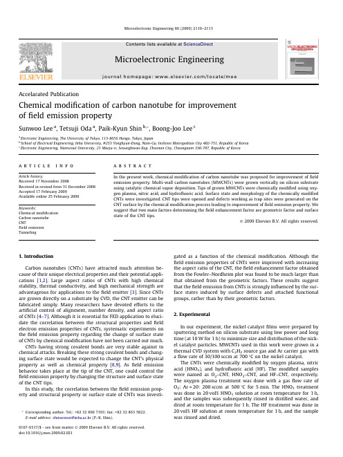
Accelarated PublicationChemical modification of carbon nanotube for improvement of field emission propertySunwoo Lee a ,Tetsuji Oda a ,Paik-Kyun Shin b,*,Boong-Joo Lee caElectronic Engineering,The University of Tokyo,113-8656Hongo,Tokyo,JapanbSchool of Electrical Engineering,Inha University,#253Yonghyun-Dong,Nam-Gu,Incheon Metropolitan City 402-751,Republic of Korea cElectronic Engineering,Namseoul University,21Maeju-ri,Seounghwan-Eup,Cheonan City,Choongnam 330-707,Republic of Koreaa r t i c l e i n f o Article history:Received 17November 2008Received in revised form 31December 2008Accepted 17February 2009Available online 25February 2009Keywords:Chemical modification Carbon nanotube CNTField emission Tunnelinga b s t r a c tIn the present work,chemical modification of carbon nanotube was proposed for improvement of field emission property.Multi-wall carbon nanotubes (MWCNTs)were grown vertically on silicon substrate using catalytic chemical vapor deposition.Tips of grown MWCNTs were chemically modified using oxy-gen plasma,nitric acid,and hydrofluoric acid.Surface state and morphology of the chemically modified CNTs were T tips were opened and defects working as trap sites were generated on the CNT surface by the chemical modification process leading to improvement of field emission property.We suggest that two main factors determining the field enhancement factor are geometric factor and surface state of the CNT tips.Ó2009Elsevier B.V.All rights reserved.1.IntroductionCarbon nanotubes (CNTs)have attracted much attention be-cause of their unique electrical properties and their potential appli-cations [1,2].Large aspect ratios of CNTs with high chemical stability,thermal conductivity,and high mechanical strength are advantageous for applications to the field emitter [3].Since CNTs are grown directly on a substrate by CVD,the CNT emitter can be fabricated simply.Many researchers have devoted efforts to the artificial control of alignment,number density,and aspect ratio of CNTs [4–7].Although it is essential for FED application to eluci-date the correlation between the structural properties and field electron emission properties of CNTs,systematic experiments on the field emission property regarding the change of surface state of CNTs by chemical modification have not been carried out Ts having strong covalent bonds are very stable against to chemical attacks.Breaking these strong covalent bonds and chang-ing surface state would be expected to change the CNT’s physical property as well as chemical property [8,9].As field emission behavior takes place at the tip of the CNT,one could control the field emission property by changing the structure and surface state of the CNT tips.In this study,the correlation between the field emission prop-erty and structural property or surface state of CNTs was investi-gated as a function of the chemical modification.Although the field emission properties of CNTs were improved with increasing the aspect ratio of the CNT,the field enhancement factor obtained from the Fowler–Nordheim plot was found to be much larger than that obtained from the geometric factors.These results suggest that the field emission from CNTs is strongly influenced by the sur-face states induced by surface defects and attached functional groups,rather than by their geometric factors.2.ExperimentalIn our experiment,the nickel catalyst films were prepared by sputtering method on silicon substrate using low power and long time (at 10W for 1h)to minimize size and distribution of the nick-el catalyst particles.MWCNTs used in this work were grown in a thermal CVD system with C 2H 2source gas and Ar carrier gas with a flow rate of 30/100sccm at 700°C on the nickel catalyst.The CNTs were chemically modified by oxygen plasma,nitric acid (HNO 3),and hydrofluoric acid (HF).The modified samples were named as O 2–CNT,HNO 3–CNT,and HF–CNT,respectively.The oxygen plasma treatment was done with a gas flow rate of O 2:Ar =20:200sccm at 500°C for 5min.The HNO 3treatment was done in 20vol%HNO 3solution at room temperature for 1h,and the samples was subsequently rinsed in distilled water,and dried at room temperature for 1h.The HF treatment was done in 20vol%HF solution at room temperature for 1h,and the sample was rinsed and dried.0167-9317/$-see front matter Ó2009Elsevier B.V.All rights reserved.doi:10.1016/j.mee.2009.02.021*Corresponding author.Tel.:+82328607393;fax:+82328635822.E-mail address:shinsensor@inha.ac.kr (P.-K.Shin).Microelectronic Engineering 86(2009)2110–2113Contents lists available at ScienceDirectMicroelectronic Engineeringjournal homepage:www.else v i e r.c o m /l o c a t e /m eeThe field emission characteristics of the grown CNT film was measured by digital multimeter in a vacuum chamber with a base pressure of 1.5Â10À8Torr.A flat parallel diode type configuration was used in the setup as shown in Fig.1.Both electrodes were glass plated with a conductive indium tin oxide (ITO)coating,and the cathode contained the grown CNT film.The distance between the anode and the CNT film surface was 100l m as separated by spacers.The surface morphology and internal structure of the CNTs were characterized by scanning electron microscopy (SEM)and trans-mission electron microscopy (TEM).3.Results and discussionsSEM images and TEM images (right side of each image)of the as-grown CNTs and the chemically modified CNTs are shown in Ts grown in this work are bamboo type multi-wall carbon nanotubes,which are vertically aligned to the substrate.The length of chemically modified CNTs is slightly shorter than that of as-grown CNTs due to the chemical etching during the chemical mod-ification processes.In case of the HNO 3–CNT,length was drastically reduced,because CNTs were partly delaminated and remained CNTs were fallen down during the chemical modification process.Tip of as-grown CNT is typically closed,while those of chemi-cally modified CNTs are opened as shown in Fig.2(right side of each image).The most parts of CNT consist of stable hexagonal car-bon structure,while the tip of CNT has pentagonal structure to close the tube end [10].The pentagonal carbon structure is easily broken by the chemical attack relative to the hexagonal structure [11].Relatively weak bonds at the CNT tip might be broken and opened by the chemical modification.Since the bond breaking might be started from the outer shell of the MWCNT used in this work and propagated into the inner shell,the shape of CNT tips be-came sharp.Furthermore,the chemical modification process might result in changing the surface state by the bond breaking as well as the structural change.In order to confirm the above mentioned surface state change,X-ray photoelectron spectroscopy (XPS)using the monochrome Al Ka X-ray was carried out.Wide scan spectra for as-grown and chemically modified CNTs are shown in Fig.3.In all cases,carbon peak (C1s,284.5eV)and oxygen peak (O1s,530eV)are observed [12].The oxygen peak stronger than that of the as-grown CNT film for the O 2–CNT,the weak nitrogen peak for HNO 3–CNT,and fluo-rine peak for HF–CNT are observed.This result correspondstoFig.1.Schematic drawing of the setup for measurement of the field emissioncurrent.Fig.2.SEM (left)and TEM (right)images of as-grown and chemically modified CNTs.S.Lee et al./Microelectronic Engineering 86(2009)2110–21132111the previous TEM results that the chemical modification processes could change the surface states of the CNT tips.The chemical modification dependence on the field emission property was investigated.Fig.4a shows emission current density as a function of applied electric field for the as-grown CNTs and the chemically modified CNTs.It is found that the chemically modified CNTs exhibit a better field emission property than that for the as-grown CNTs.If we define the threshold electric field (E th )as the ap-plied electric field that produces an emission current of 1mA/cm 2,it can be clearly seen from Fig.4b that threshold electric field is chemical modification dependent.The Fowler–Nordheim (F–N)equation can be described as,J ¼1:56Â10À6ðb E Þ2/exp À6:83Â109/3=2b E!;where J (A/cm 2)is the emission current density,E (V/l m)is theapplied electric field,b is the field enhancement factor,and /(eV)is the work function of the emitter [13].The experimental value b can be estimated on the basis of the slope of the F–N plot as shown in Fig.4c.Although there is no distinguishable difference in geo-metric factors such as diameter and length of each CNTs,the field emission property for chemically modified CNTs is better than that for as-grown CNTs.We estimated the field enhancement factors for each CNTs using geometric factors from SEM images and the FN plot of the experimental field emission data.The field enhance-ment factor estimated from the FN plot (b $1000s)was two or-ders greater than that estimated from the geometric factors (b $10s).This result implies that the field enhancement factor estimated from the F–N plot includes another factor for the improvement of field emission.Another factor affecting field emis-sion more dominantly might be correlated with the surface state of the CNT tips.TEM results and XPS results strongly imply that defects working as trap sites might be on the CNT surfaces.As shown in Fig.4c,there are two different kinds of tunneling mechanism from the slope of J /E 2vs.1/E plots.The slope at low field regime is quite dif-ferent from that at high field regime.Trap sites play a dominant role in tunneling mechanism at lower field than FN tunneling re-gime,so called trap assisted tunneling (TAT)[14].Tunneling gov-erned by TAT mechanism at low field regime affect the threshold electric field,and is related to trap sites on CNT tips.The tunneling model is based on a two-step tunneling process via traps on CNT surface which incorporates energy loss by phonon emission [15].Fig.4d shows the basic two-step process of an electron tunneling from a region with higher Fermi energy (the cathode)to a region with lower Fermi energy (the anode).Electrons could be emitted at relatively low electric field with an aid of trap sites.Finally,we suggest that two main factors determining the field enhance-ment factor are geometric factor and surface state.Therefore gen-eration of trap sites on CNT surface is strongly required to improve the field emission property,as well as the geometricfactor.Fig.3.XPS wide scan spectra of the as-grown CNTs and the chemically modified CNTs.Since some parts of CNTs are delaminated during HNO 3chemical modification process as shown in Fig.2c,strong oxygen and silicon signals are detected from the naturally oxidized Si substrate.2112S.Lee et al./Microelectronic Engineering 86(2009)2110–21134.SummaryWe have found that CNT tips were opened and defects working as trap sites were generated on the CNT surface by the chemical modification process leading to improvement of field emission property.Trap sites play a dominant role in tunneling mechanism at lower field than FN tunneling regime.We found that another factor affecting the field emission might be correlated with the sur-face state of the CNT tips.Therefore generation of trap sites on CNT surface is strongly required to improve the field emission property,as well as the geometric factor.References[1]W.A.de Heer,A.Chatelain,D.Ugarte,Science 270(1995)1179.[2]B.I.Yakobson,R.E.Smalley,Am.Sci.85(1997)324.[3]T.W.Ebbesen,Carbon Nanotubes,CRC Press,Boca Raton,FL,1997.[4]M.Chhowalla,K.B.K.Teo,C.Ducati,N.L.Rupesinghe,G.A.J.Amaratunga,A.C.Ferrari,D.Roy,J.Robertson,ne,J.Appl.Phys.90(2001)5308.[5]Y.Y.Wei,G.Eres,V.I.Merkulov,D.H.Lowndes,Appl.Phys.Lett.78(2001)1394.[6]V.I.Merkulov,D.H.Lowndes,Y.Y.Wei,G.Eres,E.Voelkl,Appl.Phys.Lett.76(2000)3555.[7]M.Katayama,K.-Y.Lee,S.Honda,T.Hirao,K.Oura,Jpn.J.Appl.Phys.43(2004)L774.[8]W.K.Hong,H.C.Shin,S.H.Tsai,et al.,Jpn.J.Appl.Phys.39(2000)L925.[9]U.D.Weglikowska,J.M.Benoit,P.W.Chiu,et al.,Curr.Appl.Phys.(2002)2.[10]G.L.Martin,P.R.Schwoebel,Surf.Sci.601(2007)1521.[11]X.Y.Zhu,S.M.Lee,Y.H.Lee,T.Frauenheim,Phys.Rev.Lett.85(2000)2757.[12]F.Moulder,W.F.Stickle,P.E.Sobol,K.D.Bomben,Handbook of X-rayPhotoelectron Spectroscopy,Physical Electronics,Inc.,Minnesota,1995.[13]R.H.Fowler,L.W.Nordheim,Proc.R.Soc.Lond.Ser.(1928)A119.[14]M.Houssa,M.Tuominen,M.Naili,V.Afanas’ev,A.Stesmans,S.Haukka,M.M.Heyns,J.Appl.Phys.87(2000)8615.[15]F.Jiménez-Molinos,A.Palma,F.Gámiz,J.Banqueri,J.A.Lopez-Villanueva,J.Appl.Phys.90(2001)3396.Fig.4.(a)J –E curves of the as-grown CNTs and the chemically modified CNTs.(b)Threshold electric field as a function of chemical modification.(c)J /E 2–1/E curves of the as-grown CNTs and the chemically modified CNTs.(d)Field emission model considering trap sites on the surface of CNT tip.S.Lee et al./Microelectronic Engineering 86(2009)2110–21132113。

碳纳米管的分类英语Carbon nanotubes are fascinating materials that come in various types. You know, there's single-walled nanotubes, which are like super-thin tubes made of a single layer of carbon atoms. They're strong and lightweight, making them great for nanoelectronics and composites.On the other hand, multi-walled nanotubes have multiple layers of carbon atoms, like a Russian nesting doll. These are more stable and can handle higher temperatures, whichis why they're often used in aerospace applications.Functionally, you've got chiral nanotubes, which have a spiral shape. They're unique in their electrical properties and can be used in sensors or as conductors in specialized electronics.But if you're looking for nanotubes that are arrangedin a specific way, there are arrayed nanotubes. Think of them like a forest of carbon nanotubes standing upright.These arrays have excellent thermal conductivity and are used in heat dissipation systems.And let's not forget about the hybrid nanotubes. These are a combination of different types, like single-walled nanotubes wrapped in another material for added properties. Hybrids are the future of carbon nanotechnology, offering endless possibilities for customization and functionality.。

碳纳米管作文二百字英文回答:Carbon nanotubes are fascinating materials that have captured the attention of scientists and engineers around the world. These nanotubes are essentially cylindrical structures made up of carbon atoms, arranged in a hexagonal pattern. They have a diameter of about one nanometer, which is incredibly small.One of the most remarkable properties of carbon nanotubes is their strength. Despite their tiny size, they are incredibly strong and can withstand a lot of pressure. This makes them ideal for applications where strength is crucial, such as in the construction of high-performance sports equipment or in the aerospace industry.Another interesting property of carbon nanotubes is their electrical conductivity. They can conduct electricity very efficiently, which makes them useful in thedevelopment of electronic devices. For example, carbon nanotubes can be used to make flexible and transparent conductive films for touchscreens or solar cells.In addition to their strength and electrical conductivity, carbon nanotubes also have unique thermal properties. They have a very high thermal conductivity, which means they can transfer heat very effectively. This makes them useful in applications where heat dissipation is important, such as in computer chips or in cooling systems for electronic devices.中文回答:碳纳米管是一种令人着迷的材料,吸引了全世界的科学家和工程师的注意。

0引言水泥是一种绝缘材料,可以通过与其它材料共混使其具有一定导电性能[1]。
碳纤维具有高强度、高模量、耐高温、耐腐蚀、抗疲劳、抗蠕变、质量轻和导电性好等特点,在水泥基体中添加短切碳纤维可以制备出碳纤维增强水泥基(CFRC )复合材料[2]。
适量碳纤维掺到水泥基体中,不仅可以提高CFRC 复合材料的拉伸塑性、粘结强度、弯曲强度和韧性,而且能够减小CFRC 的干燥收缩,从而实现在较大范围内调整CFRC 的电阻率。
其具有包括压敏性、热电效应、焦耳效应、比热容高、导热系数低、导电性好、耐蚀性好、热电性能和耐高温等优异性能[2-7]。
有研究表明[8-12],随着碳纤维掺量增加,材料的导电性能有所提高,但碳纤维掺量过高时,空隙率较大,会影响CFRC 复合材料的力学性能。
本实验采用两步法制备了碳纤维分散均匀的CFRC 复合材料。
利用扫描电镜、电阻测试仪和电子万能试验机研究了碳纤维掺量、长度和成型工艺对CFRC 复合材料力学性能和电学性能的影响。
1实验1.1原材料聚丙烯腈基短切碳纤维:上海和伍复合材料科技有限公司,长度分别为4、7、10mm ,主要性能指标见表1。
水泥:冀东水泥有限公司的P ·C32.5水泥,符合GB 175—2007要求。
分碳纤维增强水泥基复合材料的制备及其性能研究孙杰,魏树梅(内蒙古建筑职业技术学院,内蒙古呼和浩特010050)摘要:以碳纤维为增强相制备分散均匀的碳纤维增强水泥基(CFRC )复合材料,研究了碳纤维长度、掺量和成型工艺对CFRC 复合材料性能的影响。
结果表明:掺入碳纤维后,CFRC 复合材料的力学性能有所提高,电阻率明显降低;采用10mm 碳纤维、掺量为0.6%时,CFRC 复合材料的抗压强度最大提高了22.6%;碳纤维掺量相同时,碳纤维越长,电阻率越小;采用振动压实法成型试件,更有利于提高CFRC 复合材料的导电率。
关键词:碳纤维;水泥;分散;CFRC ;导电率中图分类号:TU528.58+2文献标识码:A文章编号:1001-702X (2018)10-0061-04Study on the preparation and properties of carbon fiber reinforced cement matrix compositesSUN Jie ,WEI Shumei(Inner Mongolia Technical College of Construction ,Hohhot 010050,China )Abstract :Carbon fiber reinforced cement (CFRC )composites were prepared with carbon fiber as reinforcing phase.The effectsof carbon fiber length ,content and molding process on the properties of CFRC composites were studied.The results show that compared with ordinary cement ,the mechanical properties of carbon fiber reinforced cementitious composites are improved and the resistivity decreases obviously.In CFRC composites ,when 10mm carbon fiber is used by 0.6%,the compressive strength of CFRC composites is increased by 22.6%.When the carbon fiber content is the same ,the longer the carbon fiber ,the smaller the resistivi -ty is.And the test specimen molded by vibration compaction method can improve the conductivity of CFRC composites.Key words :carbon fibre ,cement ,dispersed ,CFRC ,conductivity 收稿日期:2018-04-18;修订日期:2018-06-07作者简介:孙杰,男,1981年生,河北武安人,讲师,研究方向为土木工程、建筑工程、建筑工程管理。

碳纳米管的作文Carbon nanotubes, a remarkable material discovered in the late 20th century, have revolutionized the fields of nanotechnology and materials science. Their unique structure, consisting of carbon atoms arranged in a tubular form, confers exceptional properties such as high electrical conductivity, remarkable mechanical strength, and excellent thermal stability. These properties have made carbon nanotubes invaluable in a wide range of applications.碳纳米管,这一20世纪末发现的杰出材料,已经彻底改变了纳米技术和材料科学领域。
它们由碳原子以管状形式排列的独特结构赋予了其出色的性能,如高导电性、惊人的机械强度以及优异的热稳定性。
这些特性使得碳纳米管在众多应用中具有无可估量的价值。
In the realm of electronics, carbon nanotubes are employed as components in transistors, diodes, and other semiconductor devices. Their ability to efficiently conduct electricity makes them ideal for use in circuits, enabling faster and more efficient data transmission. Furthermore, their nanoscale dimensions allow for the creation of smaller and lighter electronic devices, paving the way for advancements in miniaturization.在电子领域,碳纳米管被用作晶体管、二极管和其他半导体器件的组成部分。

福建教育学院学报二○○三年第十期碳纳米管结构概述陈展虹(福建教育学院信息技术系,福建福州350001)摘要:本文通过对碳纳米管的分类的描述、碳纳米管的合成方法、碳纳米管结构的表征、不规则碳纳米管的结构和欧拉定律、多壁碳纳米管概述、单壁碳纳米管的管束及管束环、碳纳米管结构的稳定性以及碳纳米管结构的观察等8各方面,综述了碳纳米管的一般特点,同时提供了较详细的参考资料。
文章重点描述了碳纳米管结构的表征。
关键词:碳纳米管;结构;合成;单壁碳纳米管;多壁碳纳米管中图分类号:O6文献标识码:A陈展虹:碳纳米管结构概述前言1959年,美国著名物理学家、诺贝尔物理学奖获得者F e y nem an 曾经预言:“如果我们对物体微小规模上的排列加以某种控制的话,我们就能使物体得到大量的异乎寻常的特性,就会看到材料的性能产生丰富的变化”。
他所说的材料就是现在的纳米材料。
1990年7月在美国召开的第一届国际纳米科学技术会议,正式宣布纳米材料科学为材料科学的一个新分支。
1996年10月瑞典皇家科学院宣布,两名美国人Sm alle y 和Curl 以及一名英国人K roto 因发现C 60而荣获诺贝尔化学奖。
他们的发现发表在1985年11月份出版的《自然》杂志上[1]。
碳纳米管(Carbon nanotube )是1991年由日本电子公司(NEC )的饭岛博士(S.I i j im a )在高分子透射电镜下观察C 60结构时发现的[2]。
碳纳米管在结构上与C 60同属一类,其强度比钢高出100倍,但重量只有钢的1/6。
碳纳米管在场发射器件、电子晶体管、储氢、太阳能利用、高效催化剂以纳米生物系统等方面应用以及纳米科学与技术本身均会带来革命性的变化。
随着C 60的出现,其同族物如C 70、C 76和C 84等也先后被发现,如今又发现碳纳米管,这说明C 60及其同族物,应作为碳的第三种稳定存在的晶体结构。
因此,晶形碳有金刚石、石墨、富勒碳(巴基球以C 60为代表、碳纳米管、巴基葱)三类。


碳纳米管纤维在电化学上的应用英文回答:Carbon nanotube fibers (CNFs) have attractedsignificant interest in the field of electrochemistry due to their unique properties, including high electrical conductivity, large surface area, and excellent mechanical strength. These properties make CNFs promising candidates for a variety of electrochemical applications, such as:Electrodes for Energy Storage Devices: CNFs can be used as electrodes in supercapacitors and batteries due to their high surface area, which provides numerous active sites for electrochemical reactions. The porous structure of CNFs allows for efficient electrolyte penetration and ion transport, resulting in improved capacitance and power density.Fuel Cells: CNFs are employed as catalysts in fuelcells due to their high electrical conductivity and largesurface area. They facilitate the electrochemical reactions that occur in fuel cells, enabling efficient conversion of fuel into electricity.Biosensors: CNFs are utilized in biosensors because their large surface area can accommodate high densities of biomolecules, such as enzymes or antibodies. The electrical conductivity of CNFs allows for efficient signal transduction, making them suitable for sensitive and selective detection of analytes.Electrochemical Sensors: CNFs are used in electrochemical sensors as sensing elements due to their high sensitivity and selectivity. They can befunctionalized with specific ligands or molecules to enable selective detection of target analytes in various environments.中文回答:碳纳米管纤维在电化学上的应用:碳纳米管纤维(CNF)由于其独特的特性,如高电导率、大表面积和优异的机械强度,在电化学领域引起了广泛关注。

天津大学环境能源工程考研复习辅导资料及导师分数线信息天津大学环境能源工程考研科目包括政治、外语、数学一以及理论力学、机械原理与机械设计、内燃机原理、工程热力学、化工原理。
主要研究方向分为五个研究方向,考生可以根据自己确定的研究方向进一步了解考试科目信息。
专业代码、名称及研究方向考试科目备注0807J1环境能源工程010807J1020807J1030807J1040807J1050807J1 ①101思想政治理论②201英语一或202俄语或203日语或240德语③301数学一④801理论力学①101思想政治理论②201英语一或202俄语或203日语或240德语③301数学一④803机械原理与机械设计①101思想政治理论②201英语一或202俄语或203日语或240德语③301数学一④804内燃机原理①101思想政治理论②201英语一或202俄语或203日语或240德语③301数学一④805工程热力学①101思想政治理论②201英语一或202俄语或203日语或240德语③301数学一④826化工原理天津大学环境能源工程专业近两年考研录取情况院(系、所)专业报考人数录取人数环境能源工程无无机械工程学院(2012年)环境能源工程 2 0 机械工程学院(2013年)天津大学环境能源工程2013年报考人数为2人,录取人数0人。
由真题可以发现,现在考点涉及的广度和深度不断扩宽和加深。
由天津考研网签约的天津大学在读本硕博团队搜集整理了天津大学机械工程学院环境能源工程考研全套复习资料,帮助考生梳理知识点并构建知识框架。
真题解析部分将真题按照知识点划分,条理清晰的呈现在同学们眼前。
然后根据各个考点的近几年真题解析,让同学对热点、难点了然于胸。
只有做到了对真题规律和趋势的把握,8—10月底的提高复习才能有的放矢、事半功倍!天津大学803机械原理与机械设计考研红宝书是由天津考研网组织多名一线大学老师及过去几年在天津大学研究生初试中专业课取得高分的考生共同编写及整理的一套复习材料。


nature和science近年关于碳纳米管的文章碳纳米管是一种由碳原子构成的纳米结构,其直径约为纳米级别,长度可达微米级别。
由于其独特的结构和优异的物理化学性质,碳纳米管在材料科学、纳米技术、能源存储等领域具有广阔的应用前景。
近年来,顶级期刊Nature和Science相继发表了多篇关于碳纳米管的研究文章,本文将逐步介绍这些文章并总结其主要发现。
一、Nature上的关于碳纳米管的文章:1. “Enhanced Electrochemical Performance of Carbon Nanotube-Based Micro-Supercap acitors” (2017年)这篇文章报道了一种基于碳纳米管的微型超级电容器,通过控制碳纳米管的结构和形貌,实现了超高的电容性能。
研究者在文中详细描述了制备方法、电化学性能,以及与传统超级电容器的比较结果。
2. “Bioinspired Carbon Nanotube Transistors with Cytoskeleton-like Scaffolds”(2018年)本研究根据生物启发,通过制备具有细胞骨架类似结构的碳纳米管晶体,并将其应用于场效应晶体管中。
实验结果表明,这种生物仿生晶体管具有优异的电学性能和稳定性。
文中详细描述了合成方法、材料特性以及晶体管性能测试结果。
3. “Carbon Nanotubes as High-Performance Anode Materials for Sodium-Ion Batteries”(2019年)这篇文章探讨了碳纳米管作为钠离子电池高性能负极材料的潜力。
研究人员通过一系列实验和材料表征手段,证明了碳纳米管在钠离子电池中具有高容量、长循环寿命等优异特性。
文章中提供了详细的实验方法、电池测试结果以及相应机制的解释。
Nature上的这些文章详细描述了碳纳米管在微型超级电容器、场效应晶体管和钠离子电池等领域的应用前景和性能优势。
A Circuit Model for Carbon Nanotube Interconnects: ComparativeStudy with Cu Interconnects for Scaled TechnologiesArijit Raychowdhury and Kaushik Roy Dept of ECE, Purdue University, IN {araycho, kaushik}@Abstract: Semiconducting carbon nanotubes (CNTs) have gained immense popularity as possible successors to silicon as the channel material for ultra high performance field effect transistors. On the other hand, their metallic counterparts have often been regarded as ideal interconnects for the future technology generations. Owing to their high current densities and increased reliability, metallic-single walled CNTs (SWCNTs) have been subjects of fundamental research both in theory as well as experiments. Metallic CNTs have been modeled for RF applications in [1] using an LC model. In this paper we present an efficient circuit compatible R LC model for metallic SW CNTs, and analyze the impact of SW CNTs on the performance of ultra scaled digital VLSI design [2].I. INTRODUCTIONCarbon nanotubes [3] are sheets of graphite rolled into cylinders of diameters varying from 0.6nm to about 3nm. Depending on the direction in which they are rolled (called chirality), a CNT can be semiconducting with a distinct bandgap or it can be metallic with no bandgap. Metallic carbon nanotubes have been identified as a possible interconnect material of the future technology generations and be heir to Al and Cu interconnects. Leading theoreticians as well as experimentalists have started research in the earnest to understand the transport mechanisms and the conducting properties of the metallic CNTs [4]. Both single-walled carbon nanotubes (SWCNTs) as well as multi-walled carbon nanotubes (MWCNTs) are being investigated for performance and scalability. It has been demonstrated that MWCNTs are diffusive and have high IR drops whereas in SWCNTs, ballistic transport (drift) can be achieved and would be suitable for interconnect designs. However, in both SWCNTs and MWCNTs, very high current densities have been noted with very little performance degradation. For example, Wei et al.[5] showed that the current carrying capacity of CNTs did not degrade after 350h at current densities of ~1010 A/cm 2 at 250 °C. The thermal conductivity of CNTs [6] is about 1700–3000 W/m K. In this paper, for the first time, we envisage a realistic scenario where carbon nanotube interconnects with their intrinsic resistances and capacitances and the extrinsic (or parasitic)capacitances and inductances have been evaluated for performance. We have compared the performance of metallic SWCNTs with scaled Cu interconnects. We have used an RLC based circuit-compatible model for Cu interconnects. In the practical scenario, a damascene process is used in Cu technology to make narrow trenches and fill it up with Cu. This results in reduced interconnect dimensions and high scalability. However, it comes with the price of increased surface and grain boundary scattering. These effects have been introduced in our circuit compatible model of Cu interconnects. II. MODELING CARBON NANOTUBE INTERCONNECTSLet us consider a system of parallel carbon nanotubes, as shown in fig. 1a. Let the radius of the nanotubes be r , the separation betweennanotubes be d and let the length of a nanotube be l . We can describe the interconnect behavior of the nanotube as that of a transmission line with an RLC model as illustrated in fig. 1b and proposed in [1]. However, in [1] the diffusive component, R was not modeled and was taken to be in the ballistic limit. In such a case, the intrinsic impedance (also called the contact or quantum resistance) is given by h/ e 2 where e is the electronic charge and h is Plank's constant [7]. However, this is an optimistic assumption and under high bias or long interconnects lengths, electron-phonon interactions start to play an important role and the effects of scattering need to be incorporated.In the next three subsections, we will elaborate the R, L and C models used in our simulations.A. ResistanceRecent experiments by Ji-Yong Park et. al. [8] have measured the dc resistance of SW metallic CNTs of diameter 1.8nm (r=0.9nm). In this incoherent limit for four such channels of conduction, the differential resistance of a nanotube of length l (> Ȝ) is given by [7]: O l e h dI dV R diff ¸¹·¨©§ 24(1) where, V is the applied voltage, I is the current thorugh the CNT and Ȝ is the mean free path (mfp ). If l < Ȝ, the resistance is aconstant given by the quantum resistance for four channels (h/4e 2). The value of Ȝ is given by the scattering mechanism and isdependant on the length of the nanotube and the applied bias. For low biases (V critical <160mV), the principle scattering mechanism is due to acoustic phonons having a mfp of about 1.6µm (Ȝacc ). For higher supply biases the optical phonon (Ȝop ~ 200nm) and zone boundary phonon (Ȝzo ~30nm) scattering becomes dominant. Thus it is evident that the resistance of a CNT will be a function of thebias voltage (V bias ) as well as the length. Hence depending on the bias, the differential resistance can be expressed as:R LC Q C C(a) (b)Fig. 1: (a) Geometry of CNT (b) RLC model of parallel CNTsWe have validated this resistance model described by (2) against recently published experimental data. Fig. 2 shows how the proposed model corroborates with experimental data presented in [8] both for high as well as low voltage biases.It should be noted that eqn. (2) describes the differential resistanceof a metallic CNT. It is necessary to obtain the net (or dc)resistance of the CNT. Hence the overall dc resistance (the ratio ofthe total current, I net to the corresponding bias voltage V bias ) can bewritten as: Thus we have developed a length and bias dependant piecewise linear resistance model which has been verified with experimental data. For short lengths of the nanotube, under small bias voltages, the quantum resistance limit (or, ballistic transport) can be reached. However, for longer lengths of the current saturates to a constant value of around 25P A. We have used this resistance model forcircuit simulations using SPICE.B. InductanceTo obtain the inductance of the CNT we follow the procedure explained in reference [1,9]. Let us first consider the magnetic inductance between a CNT and the ground plane. In the presence of a ground plane, the magnetic inductance per unit length is given by [9] :This is calculated by relating the total magnetic energy and relatingit to the current flowing in the wire. For a typical situation, thenanotube is on top of an insulating (typically silicon-dioxide)substrate, with a conducting medium below. A typical oxide thickness is between 10nm and 1 P m whereas a typical nanotube radius of 1nm-2 nm. It can be noted that the magnetic inductance isa relatively weak function of the factor (h/d ) and for typical geometries it can be estimated to be around 1nH/P m.For one dimensional conductors, the kinetic inductance is as important as the magnetic inductance. The details of its derivation can be found in [1]. The kinetic inductance is given byHence, in the transmission line model (fig. 1b) we have consideredkinetic inductance only (L = L kinetic ) and have neglected magnetic inductance.C. Capacitance For CNT interconnects laid down in parallel, two distinctcapacitances would be important. One of them is the couplingelectrostatic capacitance, C C and the other is the quantum capacitance of the metallic nanotube. Equating this with the energy stored in the quantum capacitance we obtain [9]Apart from the quantum capacitance, the electrostatic capacitance is also important in parallel layout of CNT interconnects. The coupling capacitance between two CNTs each of radius r laid out at a distance d between them is given byThus we have a complete RLC model for the CNT interconnects.II. MODELING Cu INTERCONNECTSFor V< V critical: ¸¸¹·¨¨©§4¸¹·¨©§ low low diffl e h dI dV RO 24For V> V critical¸¸¹·¨¨©§4¸¹·¨©§ high highdiffl eh dI dV RO 24 where,1)( 4x for x<1=x otherwise Ȝlow = Ȝacc and Ȝhigh = (Ȝop -1+ Ȝzo -1)-1. (2a) (2b)(a) (b)Fig. 2: Differential resistance of a CNT : Validation of the proposed model with experimental data [8] : (a) for low bias (b) for high biasFor V< V critical: low diff low R RFor V> V critical 11)11( ¸¸¸¹·¨¨¨©§high diff high diff low diff bias critical highR R R V V R(3a) (3b) ¸¹·¨©§ d h L magnetic2cosh 21S P(4)F kinetic v e h L 22 ~ 16nH/µm(5) F Q hv e C 22 ~ 100 aF/µm(6) ¸¸¹·¨¨©§ ¸¹·¨©§122ln 2r d r dlC C HS(7)For the purpose of comparison, we have also modeled and simulated Cu interconnects (fig 3).A. ResistanceGrain boundary and surface scattering effects have been incorporated in a manner described in [4] to determine the resistivity of copper. The surface scattering effects can be modeled using a correction term to the intrinsic resistivity of Cu. The size dependant resistivity is given by [11]11531111)1(231 f»¼º«¬ª ¸¹·¨©§ ³dt pe e t t p k ktkt i size U U (8) where k is the ratio of the film thickness (h cu ) and the electron mean free path and p (0 p 1) is the surface scattering coefficient. Similarly the grain boundary scattering can be included in the resistivity model using13211ln 21313 »¼º«¬ª D D D D U U i grain R Rd g 1O D (9)where d g is the grain diameter, Ȝ is the electron mean free path and R (0 R 1) is the grain boundary reflection coefficient. In a manner described in [11] we have assumed p=0.6 and R=0.4. The grain boundary is also assumed to be equal to the width of the copper wire and hence d g = w cu . Hence the total resistance of each Cu wire is given byB. CapacitanceThe coupling capacitance between adjacent copper wires is given by the simple parallel plate capacitance formula)(cu cu C w d lh C H (10)C. Inductance The self inductance and mutual inductances of the Cu interconnects have been determined using the software tool MIND [12]. It involves calculation of the magnetic energy of a set of parallel wires and equating the total magnetic energy with that stored in an equivalent inductance. The details of the derivation can be found in [12] and will not be discussed here.Thus we have developed an equivalent RLC model for Cu interconnects and this has been used in comparing performance of Cu interconnects vis-à-vis CNT interconnects.III. SWITCHING DELAY USING SINGLE AND MULTIPLE CARBON NANOTUBESIn the next few sections, we will estimate the switching delay of a CNT interconnect and compare it with traditional Cu interconnect. Also the implications of scaling on CNT interconnects will bediscussed. A Single CNT interconnect First, let us consider a single CNT used as an interconnect.Consider a step input of maximum voltage 500mV to such a CNT. Fig. 4 shows the switching delay as a function of length for a single CNT interconnect. It can be noted that the switching delay for the CNT is several orders of magnitude higher than that predicted by ITRS. This is due to the large resistance of a single CNT. Even for perfect contacts and at low bias the minimum resistance of a CNT interconnect is h/(4e 2), which is approximately 6K ȍ. This resistance increases as the length of the interconnect increases and as the voltage across the CNT exceeds V critical . As a result the switching delay increases fast and far exceeds the ITRSprediction. Hence we conclude from here that a single CNT would be insufficient to act as a high speed interconnect for the future technology.B. Parallel CNT interconnectsThe next logical step would be to use CNTs in parallel that can be used to route a single signal. The corresponding layout is demonstrated in fig. 5 where N x parallel interconnects have been used as a single effective interconnect wire. It has been noted earlier that CNTs have a typical current handling capacity of 25uA/nanotube. Let us consider a current requirement of 500uA. Hence we would require 20 nanotubes in parallel (N x = 20). With a spacing of 2r (r=1.8nm) between the nanotubes, it will take a width(w = 2r(N x -1)) of 80nm. For comparison, let us consider a copper interconnect of the same width (w cu = 80nm). The maximum current handling capacity ismuch lower (J max ~ 106A/cm 2). However, the damascene process allows making deep trenches and using copper interconnects which are far deeper than they are wide. In our example, for a J maxofFig. 4: Delay vs. length of a single CNT interconnect. The ITR S prediction has been marked. Note: The length of the CNT is in meters.w cuh cuFig. 3: Layout of parallel Cu interconnects showing the interconnect dimensions. Note that h cu is the height of a Cu wire whereas h is its height from the ground plane.106A/cm2 the height, h cu needs to be 625nm in order to supply 500uA. This aspect ratio of 1:8 is easily possible in Cu technologies.Fig. 6, shows the switching delay of 20 parallel CNT interconnects and the copper interconnect (w cu = 80nm and h cu = 625nm). It can be noted that the CNT has a much higher switching delay than copper, in spite of its higher current density. This apparently counter-intuitive result can be easily understood by noting that:x Practical complementary MOS circuits are voltage driven and not current driven. In other words, the capacitors (gatecapacitance + parasistics) are charged through resistivepaths by a constant voltage source (V dd).x In voltage driven circuits the resistance of the interconnect wire and not its current density is important for performance.An ideal current source can pump a high current throughthe small cross-sectional area of the CNT. However, theresistance offered by the CNT is intrinsically high andcontrols the RLC switching delay.x The damascene process allows a high aspect ratio (ratio of h cu to w cu) of the Cu interconnects which substantiallyreduces the resistance of the Cu wire.It should thus be noted that for a voltage driven circuit the interconnect resistance and not the current density determines the switching speed.C. Oscillator frequencyIn the previous sub-sections we have considered the RLC switching delay of CNT interconnects and compared with Cu. Now let us consider a three-stage ring oscillator [13] made of scaled silicon MOSFETs. Simulations have been carried out using BPTM MOSFET models of 45nm channel length [14]. Fig. 11 shows the effect of interconnects on the frequency of oscillation.It can be observed that CNT interconnects can reduce the frequency of oscillation by orders of magnitude if the interconnect is longer than 1µm. For shorter interconnects the degradation of performance is small. If parallel CNTs are used then the effective interconnect resistance reduces. However the resistance offered by Cu interconnects is orders of magnitude smaller than CNT and it has been shown in fig. 11.IV. CONCLUSIONThis paper, for the first time, provides a realistic RLC model for CNT interconnects. Inspite of the high current density, CNT interconnects suffer from very high intrinsic resistance and kinetic inductance and severely limits high frequency of operation. Performance can be improved by routing the same signal through parallel CNTs. It has been shown that it requires a substantial increase in the number of metal layers to meet the performance of copper in the same die area. Thus CNTs provide reliable interconnect solutions but are limited in terms of performance in the high performance digital VLSI.References:[1]P. J. Burke, ‘An RF circuit model for carbon nanotubes’, IEEETrans. On Nanotech, Vol 2(1), March 2003, pp: 55-58[2]International Technology Roadmap for Semiconductors/[3]M. S. Dresselhaus et. al., Carbon nanotubes: Synthesis, structure,properties and applications, Springer, 2001.[4]Jun Li et. al., ‘Bottom-up approach for carbon nanotubeinterconnects’, Applied Physics Letters, Vol 82(15), April 2003.[5] B. Q. Wei et. al., Applied Phys. Letters. Vol 79, 1172, 2001.[6]J. Hone et. al., Physical Review. B, Vol 59, R2514, 1999.[7]S. Datta, Electronic transport in mesoscopic systems, CambridgeUniversity Press, 1995.[8]Ji-Yong, et. al., ‘Electron-Phonon scattering in metallic single-walled carbon nanotubes’ cond-mat/0309641, Sept. 28, 2003.[9]Burke, ‘Luttinger liquid theory as a model of the gigahertz electricalproperties of carbon nanotubes’, IEEE Trans. On Nanotech, Vol1(3), Sept. 2002, pp: 129-144.[10]M.W. Bockrath, “Carbon nanotubes electrons in one dimension,”Ph.D. dissertation, Univ. California, Berkeley, CA, 1999.[11]Wen Wu et. al., “Studies on size effects of copper interconnectlines’, Proc of Solid-State and Integrated-Circuit Technology, Vol. 1,Oct 2001 pp:416 – 418.[12]Zhong et. al, Proc. of Int. Conf. on Comp Design, pp. 428-433, 2002.Fig. 5: Layout of parallel CNTs. N X CNTs have been used to route the same signal. Only the 1st and the N x th CNTfeels the coupling capacitor C CFig. 6: Comparison of delay of 20 parallel CNT interconnects with copper interconnect having the same equivalent width (w=80nm). Note: The interconnect length is in meters. Fig. 7: The effect of interconnect on the oscillation frequency of a three-stage ring oscillator. Note how the CNT interconnects degrade the performance because of their high intrinsic resistance.。