半导体专业实验补充silvaco器件仿真..
- 格式:doc
- 大小:975.00 KB
- 文档页数:22
9SilvacoTCAD器件仿真模块及器件仿真流程Silvaco TCAD是一种广泛使用的集成电路(IC)设计和仿真工具,用于开发和研究半导体器件。
它提供了一套完整的器件仿真模块,可以帮助工程师设计、优化和验证各种半导体器件的性能。
本文将介绍几个常用的Silvaco TCAD器件仿真模块,并提供一个简要的器件仿真流程。
1. ATHENA模块:ATHENA是Silvaco TCAD的物理模型模拟引擎,用于模拟器件的结构和物理特性。
它可以通过解决泊松方程、电流连续性方程和能带方程等来计算电子和空穴的分布、电场和电势等物理量。
ATHENA支持多种材料模型和边界条件,可以准确地模拟各种器件结构。
2. ATLAS模块:ATLAS是Silvaco TCAD的设备模拟引擎,用于模拟半导体器件的电学和光学特性。
它可以模拟器件的电流-电压特性、载流子分布、能量带结构和光电特性等。
ATLAS支持各种器件类型,如二极管、MOSFET、BJT和太阳能电池等。
3. UTILITY模块:UTILITY是Silvaco TCAD的实用工具模块,用于处理和分析仿真结果。
它提供了各种数据可视化、数据处理和数据导出功能,帮助工程师分析和优化器件性能。
UTILITY还可以用于参数提取和模型校准,以改进模拟的准确性。
接下来是一个简要的Silvaco TCAD器件仿真流程:2. 设置模拟参数:在进行仿真之前,需要设置模拟所需的参数,如材料参数、边界条件、物理模型和仿真选项等。
可以使用Silvaco TCAD的参数设置工具来设置这些参数。
3. 运行ATHENA模拟:使用ATHENA模块进行结构模拟,通过求解泊松方程和连续性方程,计算出电子和空穴的分布、电场和电势等物理量。
可以使用Silvaco TCAD的命令行界面或图形用户界面来运行ATHENA模拟。
4. 运行ATLAS模拟:使用ATLAS模块进行设备模拟,模拟器件的电学和光学特性。
ATLAS模块可以计算器件的电流-电压特性、载流子分布、能量带结构和光电特性等。
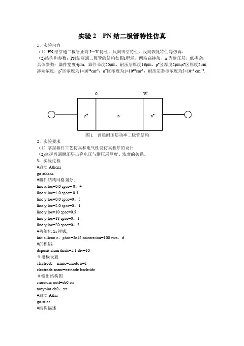
实验2 PN结二极管特性仿真1、实验内容(1)PN结穿通二极管正向I—V特性、反向击穿特性、反向恢复特性等仿真。
(2)结构和参数:PN结穿通二极管的结构如图1所示,两端高掺杂,n-为耐压层,低掺杂,具体参数:器件宽度4μm,器件长度20μm,耐压层厚度16μm,p+区厚度2μm,n+区厚度2μm.掺杂浓度:p+区浓度为1×1019cm-3,n+区浓度为1×1019cm-3,耐压层参考浓度为5×1015 cm—3.图1 普通耐压层功率二极管结构2、实验要求(1)掌握器件工艺仿真和电气性能仿真程序的设计(2)掌握普通耐压层击穿电压与耐压层厚度、浓度的关系。
3、实验过程#启动Athenago athena#器件结构网格划分;line x loc=0.0 spac= 0。
4line x loc=4.0 spac= 0.4line y loc=0.0 spac=0。
5line y loc=2.0 spac=0。
1line y loc=10 spac=0.5line y loc=18 spac=0。
1line y loc=20 spac=0。
5#初始化Si衬底;init silicon c。
phos=5e15 orientation=100 two。
d#沉积铝;deposit alum thick=1.1 div=10#电极设置electrode name=anode x=1electrode name=cathode backside#输出结构图structure outf=cb0.strtonyplot cb0。
str#启动Atlasgo atlas#结构描述doping p.type conc=1e20 x。
min=0。
0 x.max=4.0 y.min=0 y。
max=2.0 uniformdoping n.type conc=1e20 x。
min=0。
0 x。
max=4.0 y.min=18 y。


Indium Implant and Anneal1 go athena23 #TITLE: Indium Anneal45 #the x dimension definition6 line x loc = 0.0 spacing=0.17 line x loc = 0.1 spacing=0.189 #the vertical definition10 line y loc = 0 spacing = 0.0211 line y loc = 2.0 spacing = 0.201213 #initialize the mesh14 init silicon c.phos=1.0e141516 #perform uniform boron implant17 implant indium dose=1e13 energy=70 monte18 structure outfile=andfex12_0.str1920 #perform diffusion21 diffuse time=30 temperature=1000222324 extract name="xj" xj silicon mat.occno=1 x.val=0.0 junc.occno=12526 #save the structure27 structure outfile=andfex12_1.str2829 tonyplot -overlay andfex12_0.str andfex12_1.str -set andfex12.set3031 quitOxidation Enhanced Diffusion of Boron1 go athena23 # OED of Boron45 #the x dimension definition6 line x loc = 0.0 spacing=0.17 line x loc = 0.1 spacing=0.189 #the vertical definition10 line y loc = 0 spacing = 0.0211 line y loc = 2.0 spacing = 0.2012 line y loc = 25.0 spacing = 2.51314 #initialize the mesh15 init silicon c.boron=1.0e141617 #perform uniform boron implant18 implant boron dose=1e13 energy=701920 #set diffusion model for OED21 method two.dim2223 #perform diffusion24 diffuse time=30 temperature=1000 dryo225 #26 extract name="xj_two.dim" xj silicon mat.occno=1 x.val=0.0 junc.occno=12728 #save the structure29 structure outfile=andfex02_0.str3031 # repeat the simulation with default FERMI model32 go athena3334 #TITLE: Simple Boron Anneal3536 #the x dimension definition37 line x loc = 0.0 spacing=0.138 line x loc = 0.1 spacing=0.13940 #the vertical definition41 line y loc = 0 spacing = 0.0242 line y loc = 2.0 spacing = 0.2043 line y loc = 25.0 spacing = 2.54445 #initialize the mesh46 init silicon c.phos=1.0e144748 #perform uniform boron implant49 implant boron dose=1e13 energy=705051 #select diffusion model52 method fermi5354 #perform diffusion55 diffuse time=30 temperature=1000 dryo256 #57 extract name="xj_fermi" xj silicon mat.occno=1 x.val=0.0 junc.occno=1585960 #save the structure61 structure outfile=andfex02_1.str6263 # compare diffusion models64 tonyplot -overlay andfex02_0.str andfex02_1.str -set andfex02.set Emitter Push Effect1 go athena23 #TITLE: Emitter push effect example4 #5 line x loc=0.0 spac=0.26 line x loc=2.5 spac=0.87 line x loc=3.0 spac=0.28 #9 line y loc=0.00 spac=0.0410 line y loc=0.3 spac=0.0611 line y loc=2.0 spac=0.812 line y loc=10.0 spac=2.013 #14 init c.phos=1e1515 #16 implant boron dose=1e13 energy=4017 #18 deposit nitride thick=.2 div=419 #20 etch right nitride p1.x=2.521 relax y.min=1.522 #23 implant phosphor dose=1e16 energy=3024 #25 etch nitride all26 #27 method compress full.cpl28 diffuse time=30 temp=100029 #30 structure outfile=andfex07.str31 #32 tonyplot -st andfex07.str -set andfex07.set3334 quitDamage Enhanced Diffusion of ArsenicThis example demonstrates the damage enhanced diffusion effect in a heavy arsenic implant typical of MOS source/drain or bipolar emitter processing.1 go athena23 #the x dimension definition4 line x loc = 0.0 spacing=0.15 line x loc = 0.1 spacing=0.167 #the vertical definition8 line y loc = 0 spacing = 0.0059 line y loc = 2.0 spacing = 0.2010 line y loc = 25.0 spacing = 2.51112 #initialize the mesh13 init silicon c.boron=1.0e171415 #deposit screen oxide16 deposit oxide thickness=0.005 div=21718 #perform arsenic implant with damage19 implant arsenic dose=1.0e15 energy=40 tilt=7 unit.damage dam.factor=0.12021 #set diffusion model for TED22 method full.cpl2324 #perform diffusion25 diffuse time=15/60 temperature=100026 #27 extract name="xj_fullcpl" xj silicon mat.occno=1 x.val=0.0 junc.occno=12829 #save the structure30 structure outfile=andfex03_0.str3132 # repeat the simulation with FERMI model3334 #the x dimension definition35 line x loc = 0.0 spacing=0.136 line x loc = 0.1 spacing=0.13738 #the vertical definition39 line y loc = 0 spacing = 0.00540 line y loc = 2.0 spacing = 0.2041 line y loc = 25.0 spacing = 2.54243 #initialize the mesh44 init silicon c.boron=1.0e174546 #deposit screen oxide47 deposit oxide thickness=0.005 div=24849 #perform arsenic implant with damage50 implant arsenic dose=1.0e15 energy=40 tilt=7 unit.damage dam.factor=0.15152 #set default model53 method fermi5455 #perform diffusion56 diffuse time=15/60 temperature=100057 #58 extract name="xj_fermi" xj silicon mat.occno=1 x.val=0.0 junc.occno=15960 #save the structure61 structure outfile=andfex03_1.str6263 # compare diffusion models64 tonyplot -overlay andfex03_0.str andfex03_1.str -set andfex03.set。


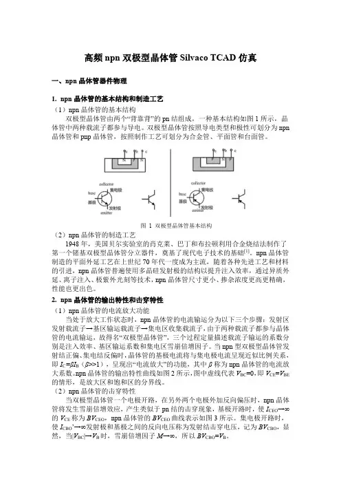
高频npn双极型晶体管Silvaco TCAD仿真一、npn晶体管器件物理1.npn晶体管的基本结构和制造工艺(1)npn晶体管的基本结构双极型晶体管由两个“背靠背”的pn结组成,一种基本结构如图1所示,晶体管中两种载流子都参与导电。
双极型晶体管按照导电类型和极性可划分为npn 晶体管和pnp晶体管,按照制作工艺可划分为合金管、平面管和台面管。
图 1 双极型晶体管基本结构(2)npn晶体管的制造工艺1948年,美国贝尔实验室的肖克莱、巴丁和布拉顿利用合金烧结法制作了第一个锗基双极型晶体管分立器件,奠基了现代电子技术的基础[1]。
npn晶体管制造的平面外延工艺在上世纪70年代一度成为主流,随着各种先进工艺和材料的引进,npn晶体管普遍使用多晶硅发射极的结构以提升注入效率,通过异质外延、离子注入、极紫外光刻等技术,npn晶体管尺寸更小、掺杂浓度更高更精确,性能也更出色。
2.npn晶体管的输出特性和击穿特性(1)npn晶体管的电流放大功能当处于放大工作状态时,npn晶体管的电流输运分为以下三个步骤:发射区发射载流子→基区输运载流子→集电区收集载流子,由于两种载流子都参与晶体管的电流输运,故得名“双极型晶体管”,三个过程定量描述载流子输运的系数分别是注入效率、基区输运系数和集电区雪崩倍增因子。
当npn型双极型晶体管发射结正偏、集电结反偏时,晶体管的基极电流将与集电极电流呈现近似比例关系,即I C=βI B(β>>1),呈现出“电流放大”的功能,其中β称为npn晶体管的电流放大系数。
npn晶体管的输出特性曲线如图2所示,图中虚线代表V BC=0,即V CE=V BE 的情形,是放大区和饱和区的分界线。
(2)npn晶体管的击穿特性当双极型晶体管一个电极开路,在另外两个电极外加反向偏压时,npn晶体管将发生雪崩倍增效应,产生类似于pn结的击穿现象,基极开路时,使I CEO→∞的V CE称为BV CEO,npn晶体管的BV CEO曲线表示如图3所示。
半导体专业实验补充silvac o器件仿真————————————————————————————————作者:————————————————————————————————日期:实验2 PN结二极管特性仿真1、实验内容(1)PN结穿通二极管正向I-V特性、反向击穿特性、反向恢复特性等仿真。
(2)结构和参数:PN结穿通二极管的结构如图1所示,两端高掺杂,n-为耐压层,低掺杂,具体参数:器件宽度4μm,器件长度20μm,耐压层厚度16μm,p+区厚度2μm,n+区厚度2μm。
掺杂浓度:p+区浓度为1×1019cm-3,n+区浓度为1×1019cm-3,耐压层参考浓度为5×1015cm-3。
0 Wp n n图1普通耐压层功率二极管结构2、实验要求(1)掌握器件工艺仿真和电气性能仿真程序的设计(2)掌握普通耐压层击穿电压与耐压层厚度、浓度的关系。
3、实验过程#启动Athenago athena#器件结构网格划分;line x loc=0.0 spac=0.4line x loc=4.0 spac= 0.4lineyloc=0.0spac=0.5line y loc=2.0 spac=0.1line y loc=10spac=0.5line y loc=18spac=0.1line y loc=20 spac=0.5#初始化Si衬底;initsilicon c.phos=5e15 orientation=100 two.d#沉积铝;deposit alum thick=1.1div=10#电极设置electrode name=anode x=1electrodename=cathode backside#输出结构图structureoutf=cb0.strtonyplotcb0.str#启动Atlasgo atlas#结构描述doping p.typeconc=1e20 x.min=0.0 x.max=4.0 y.min=0y.max=2.0 uniformdopingn.type conc=1e20x.min=0.0 x.max=4.0y.min=18y.max=20.0 uniform#选择模型和参数models cvt srh printmethod carriers=2impact selb#选择求解数值方法methodnewton#求解solve initlog outf=cb02.logsolve vanode=0.03solve vanode=0.1vstep=0.1 vfinal=5 name=anode#画出IV特性曲线tonyplot cb02.log#退出quit图2为普通耐压层功率二极管的仿真结构。
Silvaco工艺及器件仿真64.2.6 解决方案指定命令组在解决方案指定命令组中,我们需要使用Log语句来输出保存包含端口特性计算结果的记录文件,用Solving语句来对不同偏置条件进行求解,以及用Loading语句来加载结果文件。
这些语句都可以通过Deckbuild:ATLAS Test菜单来完成。
1 Vds=0.1V时,获得Id~Vgs曲线下面我们要在NMOS结构中,当Vds=0.1V时,获得简单的Id~Vgs曲线。
具体步骤如下:a.在ATLAS Commands菜单中,依次选择Solutions和Solve…项。
Deckbuild:ATLAS Test菜单将会出现,如图4.62所示;点击Prop…键以调用ATLAS Solve properties菜单;在Log file栏中将文件名改为“nmos_”,如图4.63所示。
完成以后点击OK;图4.62 Deckbuild:ATLAS Test菜单图4.63 ATLAS Solve properties菜单b.将鼠标移至Worksheet区域,右击鼠标并选择Add new row,如图4.64所示;c.一个新行被添加到了Worksheet中,如图4.65所示;d.将鼠标移至gate参数上,右击鼠标。
会出现一个电极名的列表。
选择drain,如图4.66所示;e.点击Initial Bias栏下的值并将其值改为0.1,然后点击WRITE 键;f.接下来,再将鼠标移至Worksheet区域,右击鼠标并选择Add new row;g.这样就在drain行下又添加了一个新行,如图4.67所示;h.在gate行中,将鼠标移至CONST类型上,右击鼠标并选择VAR1。
分别将Final Bias 和Delta的值改为3.3和0.1,如图4.68所示;图4.64 添加新行图4.65 添加的新行图4.66 将gate改为drain图4.67 添加另一新行图4.68 设置栅极偏置参数i.点击WRITE键,如下语句将会出现在DECKBUILD文本窗口中,如图4.69所示。
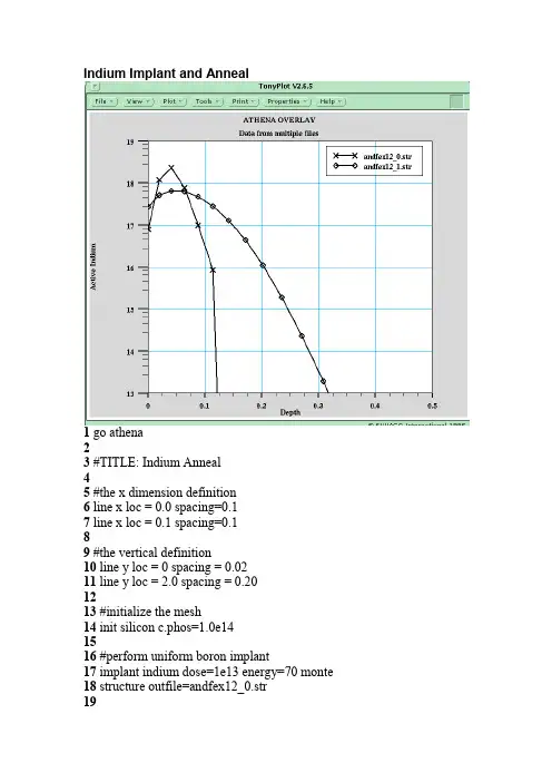
Indium Implant and Anneal1 go athena23 #TITLE: Indium Anneal45 #the x dimension definition6 line x loc = 0.0 spacing=0.17 line x loc = 0.1 spacing=0.189 #the vertical definition10 line y loc = 0 spacing = 0.0211 line y loc = 2.0 spacing = 0.201213 #initialize the mesh14 init silicon c.phos=1.0e141516 #perform uniform boron implant17 implant indium dose=1e13 energy=70 monte18 structure outfile=andfex12_0.str1920 #perform diffusion21 diffuse time=30 temperature=1000222324 extract name="xj" xj silicon mat.occno=1 x.val=0.0 junc.occno=12526 #save the structure27 structure outfile=andfex12_1.str2829 tonyplot -overlay andfex12_0.str andfex12_1.str -set andfex12.set3031 quitOxidation Enhanced Diffusion of Boron1 go athena23 # OED of Boron45 #the x dimension definition6 line x loc = 0.0 spacing=0.17 line x loc = 0.1 spacing=0.189 #the vertical definition10 line y loc = 0 spacing = 0.0211 line y loc = 2.0 spacing = 0.2012 line y loc = 25.0 spacing = 2.51314 #initialize the mesh15 init silicon c.boron=1.0e141617 #perform uniform boron implant18 implant boron dose=1e13 energy=701920 #set diffusion model for OED21 method two.dim2223 #perform diffusion24 diffuse time=30 temperature=1000 dryo225 #26 extract name="xj_two.dim" xj silicon mat.occno=1 x.val=0.0 junc.occno=12728 #save the structure29 structure outfile=andfex02_0.str3031 # repeat the simulation with default FERMI model32 go athena3334 #TITLE: Simple Boron Anneal3536 #the x dimension definition37 line x loc = 0.0 spacing=0.138 line x loc = 0.1 spacing=0.13940 #the vertical definition41 line y loc = 0 spacing = 0.0242 line y loc = 2.0 spacing = 0.2043 line y loc = 25.0 spacing = 2.54445 #initialize the mesh46 init silicon c.phos=1.0e144748 #perform uniform boron implant49 implant boron dose=1e13 energy=705051 #select diffusion model52 method fermi5354 #perform diffusion55 diffuse time=30 temperature=1000 dryo256 #57 extract name="xj_fermi" xj silicon mat.occno=1 x.val=0.0 junc.occno=1585960 #save the structure61 structure outfile=andfex02_1.str6263 # compare diffusion models64 tonyplot -overlay andfex02_0.str andfex02_1.str -set andfex02.set Emitter Push Effect1 go athena23 #TITLE: Emitter push effect example4 #5 line x loc=0.0 spac=0.26 line x loc=2.5 spac=0.87 line x loc=3.0 spac=0.28 #9 line y loc=0.00 spac=0.0410 line y loc=0.3 spac=0.0611 line y loc=2.0 spac=0.812 line y loc=10.0 spac=2.013 #14 init c.phos=1e1515 #16 implant boron dose=1e13 energy=4017 #18 deposit nitride thick=.2 div=419 #20 etch right nitride p1.x=2.521 relax y.min=1.522 #23 implant phosphor dose=1e16 energy=3024 #25 etch nitride all26 #27 method compress full.cpl28 diffuse time=30 temp=100029 #30 structure outfile=andfex07.str31 #32 tonyplot -st andfex07.str -set andfex07.set3334 quitDamage Enhanced Diffusion of ArsenicThis example demonstrates the damage enhanced diffusion effect in a heavy arsenic implant typical of MOS source/drain or bipolar emitter processing.1 go athena23 #the x dimension definition4 line x loc = 0.0 spacing=0.15 line x loc = 0.1 spacing=0.167 #the vertical definition8 line y loc = 0 spacing = 0.0059 line y loc = 2.0 spacing = 0.2010 line y loc = 25.0 spacing = 2.51112 #initialize the mesh13 init silicon c.boron=1.0e171415 #deposit screen oxide16 deposit oxide thickness=0.005 div=21718 #perform arsenic implant with damage19 implant arsenic dose=1.0e15 energy=40 tilt=7 unit.damage dam.factor=0.12021 #set diffusion model for TED22 method full.cpl2324 #perform diffusion25 diffuse time=15/60 temperature=100026 #27 extract name="xj_fullcpl" xj silicon mat.occno=1 x.val=0.0 junc.occno=12829 #save the structure30 structure outfile=andfex03_0.str3132 # repeat the simulation with FERMI model3334 #the x dimension definition35 line x loc = 0.0 spacing=0.136 line x loc = 0.1 spacing=0.13738 #the vertical definition39 line y loc = 0 spacing = 0.00540 line y loc = 2.0 spacing = 0.2041 line y loc = 25.0 spacing = 2.54243 #initialize the mesh44 init silicon c.boron=1.0e174546 #deposit screen oxide47 deposit oxide thickness=0.005 div=24849 #perform arsenic implant with damage50 implant arsenic dose=1.0e15 energy=40 tilt=7 unit.damage dam.factor=0.15152 #set default model53 method fermi5455 #perform diffusion56 diffuse time=15/60 temperature=100057 #58 extract name="xj_fermi" xj silicon mat.occno=1 x.val=0.0 junc.occno=15960 #save the structure61 structure outfile=andfex03_1.str6263 # compare diffusion models64 tonyplot -overlay andfex03_0.str andfex03_1.str -set andfex03.set。
§4 工艺及器件仿真工具SILVACO-TCAD本章将向读者介绍如何使用SILVACO公司的TCAD工具ATHENA来进行工艺仿真以及ATLAS来进行器件仿真。
假定读者已经熟悉了硅器件及电路的制造工艺以及MOSFET和BJT 的基本概念。
使用ATHENA的NMOS工艺仿真4.1.1 概述本节介绍用ATHENA创建一个典型的MOSFET输入文件所需的基本操作。
包括:a. 创建一个好的仿真网格b. 演示淀积操作c. 演示几何刻蚀操作d. 氧化、扩散、退火以及离子注入e. 结构操作f. 保存和加载结构信息4.1.2 创建一个初始结构1 定义初始直角网格a. 输入UNIX命令:deckbuild-an&,以便在deckbuild交互模式下调用ATHENA。
在短暂的延迟后,deckbuild主窗口将会出现。
如图所示,点击File目录下的Empty Document,清空DECKBUILD文本窗口;图清空文本窗口b. 在如图所示的文本窗口中键入语句go Athena ;图以“go athena”开始接下来要明确网格。
网格中的结点数对仿真的精确度和所需时间有着直接的影响。
仿真结构中存在离子注入或者形成PN结的区域应该划分更加细致的网格。
c. 为了定义网格,选择Mesh Define菜单项,如图所示。
下面将以在μm×μm的方形区域内创建非均匀网格为例介绍网格定义的方法。
图调用ATHENA网格定义菜单2 在μm×μm的方形区域内创建非均匀网格a. 在网格定义菜单中,Direction(方向)栏缺省为X;点击Location(位置)栏并输入值0;点击Spacing(间隔)栏并输入值;b. 在Comment(注释)栏,键入“Non-Uniform Grid x ”,如图所示;c. 点击insert键,参数将会出现在滚动条菜单中;图定义网格参数图点击Insert键后d. 继续插入X方向的网格线,将第二和第三条X方向的网格线分别设为和,间距均为。
实验2 PN结二极管特性仿真1、实验内容(1)PN结穿通二极管正向I-V特性、反向击穿特性、反向恢复特性等仿真。
(2)结构和参数:PN结穿通二极管的结构如图1所示,两端高掺杂,n-为耐压层,低掺杂,具体参数:器件宽度4μm,器件长度20μm,耐压层厚度16μm,p+区厚度2μm,n+区厚度2μm。
掺杂浓度:p+区浓度为1×1019cm-3,n+区浓度为1×1019cm-3,耐压层参考浓度为5×1015 cm-3。
图1 普通耐压层功率二极管结构2、实验要求(1)掌握器件工艺仿真和电气性能仿真程序的设计(2)掌握普通耐压层击穿电压与耐压层厚度、浓度的关系。
3、实验过程#启动Athenago athena#器件结构网格划分;line x loc=0.0 spac= 0.4line x loc=4.0 spac= 0.4line y loc=0.0 spac=0.5line y loc=2.0 spac=0.1line y loc=10 spac=0.5line y loc=18 spac=0.1line y loc=20 spac=0.5#初始化Si衬底;init silicon c.phos=5e15 orientation=100 two.d#沉积铝;deposit alum thick=1.1 div=10#电极设置electrode name=anode x=1electrode name=cathode backside#输出结构图structure outf=cb0.strtonyplot cb0.str#启动Atlasgo atlas#结构描述doping p.type conc=1e20 x.min=0.0 x.max=4.0 y.min=0 y.max=2.0 uniformdoping n.type conc=1e20 x.min=0.0 x.max=4.0 y.min=18 y.max=20.0 uniform#选择模型和参数models cvt srh printmethod carriers=2impact selb#选择求解数值方法method newton#求解solve initlog outf=cb02.logsolve vanode=0.03solve vanode=0.1 vstep=0.1 vfinal=5 name=anode#画出IV特性曲线tonyplot cb02.log#退出quit图2为普通耐压层功率二极管的仿真结构。
正向I-V特性曲线如图3所示,导通电压接近0.8V。
图2 普通耐压层功率二极管的仿真结构图3 普通耐压层功率二极管的正向I-V特性曲线运用雪崩击穿的碰撞电离模型,加反向偏压,刚开始步长小一点,然后逐渐加大步长。
solve vanode=-0.1 vstep=-0.1 vfinal=-5 name=anodesolve vanode=-5.5 vstep=-0.5 vfinal=-20 name=anodesolve vanode=-22 vstep=-2 vfinal=-40 name=anodesolve vanode=-45 vstep=-5 vfinal=-240 name=anode求解二极管反向IV特性,图4为该二极管的反向I-V特性曲线。
击穿时的纵向电场分布如图5所示,最大电场在结界面处,约为2.5×10⁵V•cm-1,在耐压层中线性减小到80000 V•cm-1。
图4 普通耐压层功率二极管的反向I-V特性曲线图5 普通耐压层功率二极管击穿时的电场分布导通的二极管突加反向电压, 需要经过一段时间才能恢复反向阻断能力。
电路图如图6所示。
设t= 0 前电路已处于稳态,I d= I f0。
t= 0 时,开关K 闭合,二极管从导通向截止过渡。
在一段时间内,电流I d以d i0/ d t = - Ur/ L 的速率下降。
在一段时间内电流I d会变成负值再逐渐恢复到零。
仿真时先对器件施加一个1V的正向偏压,然后迅速改变电压给它施加一个反向电压增大到2V。
solve vanode=1log outf=cj2_1.logsolve vcathode=2.0 ramptime=2.0e-8 tstop=5.0e-7 tstep=1.0e-10反向恢复特性仿真时,也可以采用如图7的基本电路,其基本原理为:在初始时刻,电阻R1的值很小,电阻R2的值很大,例如可设R1为1×10⁻³Ω,R2为1×10⁶Ω;电感L1可设为3nH;电压源及电流源也分别给定一个初始定值v1,i1;那么由于R2远大于R1,则根据KCL可知,电流i1主要经过R1支路,即i1的绝大部分电流稳定的流过二极管,二极管正向导通,而R2支路几乎断路,没有电路流过。
然后,在短暂的时间内,使电阻R2的阻值骤降。
此时,电阻器R2作为一个阻源,其阻值在极短的时间间隔内以指数形式从1×10⁶Ω下降到1×10⁻³Ω。
这一过程本质上是使与其并联的连在二极管阳极的电流源i1短路,这样电流i1几乎全部从R2支路流过,而二极管支路就没有i1的分流,此刻电压源v1开始起作用,二极管两端就被施加了反偏电压,由于这些过程都在很短的时间内完成,因而能够很好的实现二极管反向恢复特性的模拟。
反向恢复特性仿真图如图8所示,PN结功率二极管的反向恢复时间约为50ns。
图6 反向恢复特性测试原理电路图R1R2L1二极管独立电流源i1独立电压源V1+-+-图7 二极管反向恢复特性模拟电路图图8 器件反向恢复特性曲线实验3 PN结终端技术仿真1、实验内容由于PN结在表面的曲率效应,使表面的最大电场常大于体内的最大电场,器件的表面易击穿,采用终端技术可使表面最大电场减小,提高表面击穿电压。
场限环和场板是功率器件中常用的两种终端技术。
场限环技术是目前功率器件中被大量使用的一种终端技术。
其基本原理是在主结表面和衬底之间加反偏电压后,主结的PN结在反向偏压下形成耗尽层,并随着反向偏置电压的增加而增加。
当偏置电压增加到一定值是,主结的耗尽层达到环上,如图1所示,这样就会使得有一部分电压有场环分担,将主结的电场的值限制在临界击穿电压以内,这将显著的减小主结耗尽区的曲率,从而增加击穿电压。
图1 场限环场板结构在功率器件中被广泛应用。
场板结构与普通PN结的区别在于场板结构中PN 区引线电极横向延伸到PN区外适当的距离。
而普通PN结的P区引线电极的横向宽度一般不超过P扩散区的横向尺寸。
PN结反向工作时,P区相对于N型衬底加负电位。
如果场板下边的二氧化硅层足够厚,则这个电场将半导体表面的载流子排斥到体内,使之表面呈现出载流子的耗尽状态,如图2所示,就使得在同样电压作用下,表面耗尽层展宽,电场减小,击穿电压得到提高。
2、实验要求(1)场限环特性仿真场限环:击穿电压200V,设计3个环,环的宽度依次为6、5、5、5μm,间距为4、5、6μm, 外延层浓度为1×1015 cm-3,观察表面电场。
(2)场板特性仿真场板:氧化层厚度1μm,结深1μm,场板长度分别为0μm、2μm、4μm、6μm、8μm、10μm,外延层浓度为1×1015 cm-3,观察表面电场。
图2 场板3、场板的应用实例:场板对大功率GaN HEMT击穿电压的影响(1)内容(a)GaN HEMT的工作机理、击穿特性刻画以及对场板结构的GaN HEMT击穿特性的进行仿真分析。
(b)结构和参数:场板结构的GaN HEMT的结构尺寸及掺杂浓度如图3所示。
图3 场板结构的大功率GaN HEMT(2) 要求(a)掌握定义一个完整半导体器件结构的步骤,并能对其电性能进行仿真研究。
(b)理解场板技术对器件击穿电压提高的作用原理并能结合仿真结果给出初步分析。
(3)实验过程#启动internal,定义结构参数# 场板长度从1um增大到2.25um,步长为0.25um,通过改变l 取值来改变场板长度set l= 1.0# drain-gate distanceset Ldg=5.1# field plate thicknessset t=1.77355# AlGaN composition fractionset xc=0.295# set trap lifetimeset lt=1e-7set light=1e-5# mesh locations based on field plate geometryset xl=0.9 + $lset xd=0.9 + $Ldgset y1= 0.3 + $tset y2= $y1 + 0.02set y3= $y2 + 0.04set y4= $y2 + 0.18# 启动二维器件仿真器go atlasmesh width=1000# 网格结构x.m l=0.0 s=0.1x.m l=0.05 s=0.05x.m l=0.5 s=0.05x.m l=0.9 s=0.025x.m l=(0.9+$xl)/2 s=0.05x.m l=$xl s=0.025x.m l=($xl+$xd)/2 s=0.25x.m l=$xd-0.05 s=0.05x.m l=$xd s=0.05#y.m l=0.0 s=0.1000y.m l=0.3 s=0.1000y.m l=$y1 s=0.0020y.m l=$y2 s=0.0020y.m l=$y3 s=0.0100y.m l=$y4 s=0.0500# device structure# POLAR.SCALE is chosen to match calibrated values# of 2DEG charge concentrationregion num=1 mat=SiN y.min=0 y.max=$y1region num=2 mat=AlGaN y.min=$y1 y.max=$y2 donors=1e16 p=$xc polar calc.strain polar.scale=-0.5region num=3 mat=GaN y.min=$y2 y.max=$y4 donors=1e15 polar calc.strain polar.scale=-0.5#elect name=source x.max=0 y.min=$y1 y.max=$y3elect name=drain x.min=6.0 y.min=$y1 y.max=$y3elect name=gate x.min=0.5 x.max=0.9 y.min=0.3 y.max=$y1elect name=gate x.min=0.5 x.max=$xl y.min=0.3 y.max=0.3#doping gaussian characteristic=0.01 conc=1e18 n.type x.left=0.0 \x.right=0.05 y.top=$y1 y.bottom=$y3 teral=0.01 direction=y doping gaussian characteristic=0.01 conc=1e18 n.type x.left=$xd-0.05 \x.right=$xd y.top=$y1 y.bottom=$y3 teral=0.01 direction=y#################################################################### KM parameter set###################################################################material material=GaN eg300=3.4 align=0.8 permitt=9.5 \mun=900 mup=10 vsatn=2e7 nc300=1.07e18 nv300=1.16e19 \real.index=2.67 imag.index=0.001 \taun0=$lt taup0=$ltmaterial material=AlGaN affinity=3.82 eg300=3.96 align=0.8 permitt=9.5 \mun=600 mup=10 nc300=2.07e18 nv300=1.16e19 \real.index=2.5 imag.index=0.001 \taun0=$lt taup0=$lt###################################################################model print fermi fldmob srhimpact material=GaN selb an1=2.9e8 an2=2.9e8 bn1=3.4e7 bn2=3.4e7 \ap1=2.9e8 ap2=2.9e8 bp1=3.4e7 bp2=3.4e7#contact name=gate work=5.23# 人为引进光照以利于实现阻断状态下仿真收敛,这是仿真研究击穿的常用手段beam number=1 x.o=0 y.o=$y4+0.1 angle=270 wavelength=0.3#output con.band val.band band.param charge e.mob h.mob flowlines qss# IdVg特性求解solvelog outf=ganfetex02_0.logsolve vdrain=0.05solve vstep=-0.2 vfinal=-2 name=gatesolve vstep=-0.1 vfinal=-4 name=gatelog offsave outfile=ganfetex02_0.strextract init infile="ganfetex02_0.log"extract name="Vpinchoff" xintercept(maxslope(curve(v."gate",i."drain")))# IdVd击穿曲线method autonr gcarr.itlimit=10 clim.dd=1e3 clim.eb=1e3 nblockit=25solve init# turn on optical source to help initiate breakdown# # 人为引进光照以利于实现阻断状态下仿真收敛solve b1=$light index.check#solve nsteps=10 vfinal=$Vpinchoff name=gate b1=$lightlog outf=ganfetex02_$'index'.logsolve vstep=0.1 vfinal=1 name=drain b1=$lightsolve vstep=1 vfinal=10 name=drain b1=$lightsolve vstep=2 vfinal=20 name=drain b1=$lightsolve vstep=5 vfinal=1200 name=drain b1=$light cname=drain compl=0.5# change to current contact to resolve breakdowncontact name=drain currentsolvesolve imult istep=1.1 ifinal=1 name=drain#save outfile=ganfetex02_$'index'.str#extract init infile="ganfetex02_1$'index'.log"extract name="a" slope(maxslope(curve(i."drain",v."drain")))extract name="b" xintercept(maxslope(curve(i."drain",v."drain")))extract name="Vdmax" max(curve(i."drain",v."drain"))extract name="Idmax" x.val from curve(i."drain",v."drain") where y.val=$Vdmaxextract name="Vd1" $Vdmax - 20extract name="Id1" y.val from curve(v."drain",i."drain") where x.val=$Vd1extract name="c" grad from curve(v."drain",i."drain") where x.val=$Vdmaxextract name="d" $Idmax - $c*$Vdmaxextract name="Vbr" ($b - $d)/($c - (1/$a))extract name="Is" $b + $Vbr/$atonyplot ganfetex02_1.str ganfetex02_2.str ganfetex02_3.str ganfetex02_4.str ganfetex02_5.str ganfetex02_6.str -set ganfetex02_1.settonyplot -overlay ganfetex02_1.log ganfetex02_2.log ganfetex02_3.log ganfetex02_4.log ganfetex02_5.log ganfetex02_6.log -set ganfetex02_0.setquit图4-9为不同场板长度下半导体层中碰撞离化率的分布图。