CMOS Detector Technology
- 格式:ppt
- 大小:3.07 MB
- 文档页数:17

键鼠产品专业术语全面解析前言:键盘鼠标是大家每天接触最多的电脑配件之一,作为最主要的输入工具,键鼠早已是每部电脑不可或缺的一部分。
另外,还有为数不少的外设爱好者,喜欢各种精美的键鼠,常常活跃在外设论坛。
于是,我们经常听到DPI、FPS等等关于键鼠的术语,到底它们代表什么意思呢?今天我们就一起来次大充电吧!一、各类鼠标引擎工作原理传统光学鼠标的工作原理传统光学鼠标工作原理示意图光学跟踪引擎部分横界面示意图光学鼠标主要由四部分的核心组件构成,分别是发光二极管、透镜组件、光学引擎(Optical Engine)以及控制芯片组成。
光学鼠标通过底部的LED灯,灯光以30度角射向桌面,照射出粗糙的表面所产生的阴影,然后再通过平面的折射透过另外一块透镜反馈到传感器上。
什么是激光鼠标?学过物理学的朋友都知道,光具有波粒二象性,干涉和衍射特性就是激光鼠标产生的灵感和起源。
激光鼠标其实也是光电鼠标,只不过是用激光代替了普通的LED光.好处是可以通过更多的表面,因为激光是Coherent Light(相干光),几乎单一的波长,即使经过长距离的传播依然能保持其强度和波形;而LED光则是Incoherent Light(非相干光)。
激光鼠标传感器获得影像的过程是根据,激光照射在物体表面所产生的干涉条纹而形成的光斑点反射到传感器上获得的,而传统的光学鼠标是通过照射粗糙的表面所产生的阴影来获得。
因此激光能对表面的图像产生更大的反差,从而使得“CMOS成像传感器”得到的图像更容易辨别,提高鼠标的定位精准性。
罗技“DARK FIELDFIELD””无界激光引擎罗技“DARK FIELD”无界激光引擎罗技Darkfield无界技术采用暗视野显微来探测表面上的微观颗粒和微小的划痕,而不是追踪表面本身。
与我们的眼睛能够看清夜晚的天空一样,鼠标的传感器将洁净的玻璃视为有着许多亮点的黑色背景,而这些亮点就是灰尘。
然后,传感器能够通过这些点的运动精确追踪鼠标的移动。


基于CMOS工艺SPAD的单光子探测技术研究重庆大学硕士学位论文(学术学位)学生姓名:***指导教师:孟丽娅副教授专业:仪器科学与技术学科门类:工学重庆大学光电工程学院二O一五年五月中央高校科研基本业务费资助项目(CDJZR12120001)Study on single-photon detector Based on CMOS Technology Single-Photon AvalancheDiodeA Thesis Submitted to Chongqing UniversityIn Partial Fulfillment of the Requirement for theMaster’s Degree of EngineeringByYan XuliangSupervised by Associate Prof. Meng LiyaSpecialty: Instrument Science and TechnologyCollege of Optoelectronic Engineering of ChongqingUniversity, Chongqing, ChinaMay, 2015Supported by CDJZR(No.12120001)中文摘要摘要光在极其微弱时会离散成一个个的光子,称为单光子。
单光子信号由于强度微弱且粒子性显著,常规技术难以对其检测,被认为是光电探测技术的极限。
同时单光子信号又是一种普遍存在的信息载体,在日常生活、工业生产、科学研究以及国防军事等各方面都有着广泛应用,因而近年来受到研究人员重视。
单光子探测技术主要体现在以下几方面:有极高增益的单光子探测器件,控制单光子探测器件并对信号进行处理的快速电路,器件和电路的集成技术,大规模像元阵列的制作及拼接。
目前在单光子探测方面亟待解决的问题有:单光子探测器工艺复杂、工作电压高、价格昂贵、重复性差,外围电路响应速度慢、版图面积大,对单光子探测器和相关电路的混合拼接易导致性能下降、噪声变大。

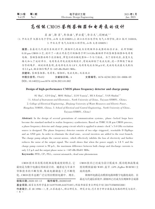
应用于脉冲TOF成像LADAR系统的高性能CMOS全差分放大器设计蒋衍;刘汝卿;朱精果;王宇【摘要】本文设计了一种应用于脉冲飞行时间(TOF)成像激光雷达探测系统的高带宽、低噪声全差分放大器(FDMA).该芯片采用多级级联结构和有源电感技术,增大电路带宽和减少芯片面积,并且通过使用失调隔离技术,增强了各增益级对工艺偏差的鲁棒性.在输出级电路中,为使全差分放大器具有更强的驱动能力,采用了宽带放大器和输出缓冲器级联结构做为输出.同时,为了满足激光雷达系统的实际需求,采用复用失调隔离电路的方式,实现了级间带通滤波来限制放大器的适用带宽.采用CMSC 的CMOS工艺进行了FDMA流片.测试结果表明,该芯片具有730.6 MHz的-3 dB 带宽,在使用带通滤波器优化后的开环增益为23.5 dB,等效输入噪声密度为2.7 nV/sqrt(Hz),有效地降低了系统噪声.芯片采用3.3 V电源供电,功耗为102.3 mW,整体面积为0.25 mm×0.25 mm.作为激光雷达全系统集成芯片中的一部分,较好地满足系统指标要求.【期刊名称】《光电工程》【年(卷),期】2019(046)007【总页数】8页(P61-68)【关键词】激光雷达接收器;全差分放大器;级联式增益级;有源电感【作者】蒋衍;刘汝卿;朱精果;王宇【作者单位】中国科学院微电子研究所,北京 100029;中国科学院大学,北京100049;中国科学院微电子研究所,北京 100029;中国科学院微电子研究所,北京100029;中国科学院微电子研究所,北京 100029【正文语种】中文【中图分类】TB872As an optical remote sensing technology, the laser detection and ranging (LADAR) system has been used in many fields[1-3], including the auxiliary driving, intelligent robot for target identification, and the 3D imaging. The pulsed time-of-flight (TOF) LADAR system that measures the distances to targets by emitting and detecting laser echoes accurately has the unique advantage of long detection range compared to other measurement methods such as the continuous-wave optical phase method[4-5].A block diagram of a typical TOF LADAR system is shown in Fig. 1. As shown in the figure, the LADAR system is composed of a pulsed laser transmitter, an amplifier receiver, a time-to-digital converter (TDC), an analog-digital converter (ADC), and a micro-processor. The pulsed laser transmitter generates a start signal and simultaneously emits an optical pulse signal. After focused by some optical components, the laser pulse signal launches towards the target, and an echo signal will be produced and reflected back when the optical pulse encounters the target. The amplifier receiver, on which this paper focuses, amplify the reflection signal f rom the target by receiver’s optical component to the analog-digital converter, and generates the arrival timing signal (stop) of the echo signalto the time-to-digital converter[6]. In the signal processor, according to the flight time, the distance between the target and the receiver can be calculated through the LADAR formulas by using the micro-processor. The amplifier receiver which mainly includes a photoelectric detector and analog front-end circuits converts the optical pulse echo signal into an electrical pulse. The photoelectric detector usually employs an avalanche photodiode (APD) because of the high sensitivity. The analog front-end circuits, which mainly consist a trans-impedance amplifier (TIA) and a main amplifier, are used to convert a current signal to a voltage signal for the analog-digital converter and time-to-digital converter to discriminate. However, only by using TIA it cannot satisfy the demand for the remote detection applications. Since the transmit power of the pulse laser are limited, in active imaging system, the performance of the main amplifier becomes a critical issue. Therefore, a high-performance main amplifier is a key component to the LADAR system.In this paper, a fully differential main amplifier chip has been implemented in a CSMC CMOS process. The proposed amplifier applied active inductor, which is used to reduce the chip area and enlarge the bandwidth of the circuit. In order to apply for LADAR system, this work achieves an inter-stage bandpass filter by reusing the DC offset isolation circuit. Section 2 describes the LADAR system and proposed amplifier receiver. Section 3 introduces the details of fully differential main amplifier. The measurement results of the chip are shown in Section 4, and Section 5 summarizes the design.The amplifier receiver is mainly to amplify the moment of the weak optical echo signal which is come from the target. The input current signal of the photoelectric detector produced can be acquired by the well-known radar principle and responsibility of APD.where is the responsibility of APD, is the peak power of the laser transmitted pulse, is the transmission of the optical system, means the reflection coefficient of the target, is the active area of the receiver lens. Last, and is the distance between the target and receiver.Usually, an avalanche PD (APD) is used as the photodetector because of the high responsivity. The gain of a Si APD can be 50 A/W, but the InGaAs APD has the typical gain of only 10 A/W. Therefore, the minimum detectable echo signal for the receiver will be only few tens of nW by using InGaAs APD.The signal-to-noise ratio (SNR) can be calculated by the radar formula[7]. In order to suitable the practical applications, the requirement of the SNR is over 5 in the general hundreds of meter detection LADAR system. Further, the SNR over 10 would be advantageous for mm-level accuracy. Figure 2 shows the block diagram of the proposed amplifier receiver. In Fig. 2, the proposed amplifier receiver consists of two parts: trans impedance amplifier (TIA) and main amplifier. The TIA is an analog circuit that converts the input current pulse signal from the APD into voltage. And the main amplifier’s task is to further amplify the small voltage signal to an appropriate level so that the voltage can be process by the followed circuit such as the TDC and ADC. However, only by using TIA it cannot satisfy thedemand of the voltage for the remote detection system. Therefore, the performance of the main amplifier influences the optical pulse receiver largely.The main amplifier circuit should have enough wide bandwidth to keep the pulse waveform linearly magnified. However, excessive bandwidth would lead to additional noise entering the receiver, due to the signal-to-noise ratio (SNR) of the receiver deteriorated. The bandwidth (BW) as a critical limit can be approximately expressed as follows[8]:where tr is the rise edge of the time signal. For general applications, the pulsed laser with a peak power of 20 W ~75 W and a width of 3 ns~20 ns is needed[9]. This means that a narrower pulsed echo requires about 100 MHz ~200 MHz BW of the whole receiver channel. In the design, BW of the fully differential main amplifier (FDMA) is demanded over the 500 MHz. At the same time, in order to meet the LADAR system application, this work designs an inter-stage bandpass filter by reusing the DC offset isolation circuit to limit system noise.The structure of the fully differential main amplifier (FDMA) is presented in Fig. 3. In the diagram, the circuit includes four identical gain stages to provide enough voltage gain, a large bandwidth amplifier (LBA) and an output buffer (OB) stage to enhance the deriver ability, and the bandpass filter to limit noise. In order to keep the walk error of the LADAR system small, the bandwidth of amplifier stages must be sufficiently wide frequency range. The stages need to operate linearly and resume rapidly enough after the signal inputting. This circuit is achieved by using severalamplifiers chain with a high slew rate and a large bandwidth. However, excessive bandwidth would cause additional noise entering the receiver, which degrades the receiver’s signal-to-noise ratio (SNR). Therefore, the bandwidth of the whole amplifier chains should be confined. Meanwhile, the inter-stage bandpass filter which reuses the DC offset isolation circuit to limit system noise and mitigates the problem that the coupled capacitances occupy a large area in CMOS process and lead to attenuate the signal should be carefully designed. In addition, the cascaded gain stage (CGS) that realized by four identical gain stages would deteriorate the amplifiers bandwidth. Therefore, this work adopts the active inductor technology instead of traditional spiral inductor architecture to extend bandwidth. By using the method, the bandwidth of single stage is extend up to 70% without deteriorating the frequency response[10].In conventional integrated amplifier systems, the cascaded gain stage (CGS) is widely used to achieve optimum results for both high gain and wide bandwidth. Assuming that the circuit consists ofnidenticalgain stages with one pole frequency response, for the multilevel cascaded gain stages, the total bandwidth can be calculated as following (3):where BWs is the bandwidth of each gain stage, and BWtol is the whole bandwidth of CGS. Therefore, the gain bandwidth product of each gain stage given by (4):where Atol is the total gain of CGS, and GBWs is the gain bandwidth product of each gain stage.According to above formulas, there are shown that the increasing numberof the gain stages can directly achieve higher gain. Consequently, the simplest way to enlarge the cascaded gain bandwidth product is to make the number of stages as larger as possible. However, this approach will not only result in a significant increase in the power consumption and area, but also make a rapid accumulation of noise from the gain stage, which has a significant impact on the amplifier circuit stability. In the practical design, the maximum number of stages is usually limited to below five[11]. In the designed pulsed TOF imaging LADAR system, the proposed FDMA needs to meet the requirements as following:, . For n=4, it can be calculated that the BWsshould exceed 1.4 GHz and each stage should have a gain of approximately 5.25 dB. Therefore, considering the gain bandwidth and noise figure, the CGS which contains four the same gain stages is designed in the paper.The element structure of the main amplifier is the fully differential cascaded stage. However, it is hard to achieve such a wide bandwidth based on CMSC 0.5 μm CMOS process. The active inductor technique is adopted to alleviate the bandwidth degradation, because the spiral inductor with a high inductance will occupy a lot of area and it is difficult to implement in CMOS process[12]. Fig. 4 shows the structure of the proposed CGS with an active inductor load.The simplified small-signal analysis model of the active inductor load, which consists of a MOS transistor M4 and a resistor Rg, is shown in Fig. 5. Usually, there are , and , so that the Cgd4, Cds4, gds4 can be neglected. The equivalent impedance of the active inductor can be given asfollowing[13]:where Zin is the output impedance. Cgs4 is the gate-source capacitance of MOS transistor, and gm4 is the trans-conductance of MOS transistor. Therefore, the equivalent inductance L and resistance R can be calculated as following[14]:The ωT is the unity current gain angular frequency. In order to avoid undesirable peaking on the frequency response, the resistance Rg should be designed carefully according to the capacitive load of the following stage. The active inductors perform an impedance of Rg at low frequency. When the frequency is sufficiently high, the inductor L is formed by Rg and Cgs4 so that the impedance of the gain stage is increased. The impedance change is similar to the inductor and the frequency within a certain range[15]. The gain of the common source amplifier that has a structure of the active inductor load can be expressed as following (7):The for mula reveals that the stage’s gain only has received the influences on the dimension of the input and load transistors. Consequently, the circuit that uses the active inductor structure has stronger capacity against to the alteration of temperature and process. Besides, the formula can be obtained as (8):Through choosing the appropriate value of the L and R, the bandwidth can be extended largely while maintaining a suppressed gain peak over the frequency range. In summary, based on the above formula, the CGS that consists of four identical gain stages and active inductive load is the optimized choice for this design.During chip fabrication, many non-ideal elements such as the asymmetry layout design and slight deviations in MOS transistor will result in DC offset, especially for cascaded differential gain structure. Since the amplifier that uses the multi-stage cascade structure as a high gain, the DC offset voltage which generated by the preamplifier unit is amplified, resulting in a large shift of the operating point of the post amplifier[16]. Even if the input deviation is small, the amplification of the stages may cause the output buffer to reach the saturation.In order to stabilize the operating point and DC gain, the structure of offset voltage compensation loop is required. This circuit employs capacitive coupling to eliminate DC offset. As shown in Fig. 6, C1 and C2 are DC blocking capacitors for eliminating DC offset. Ma1~Ma8(Mb1~Mb8) are NMOS transistors with the same substrate and source terminals to provide a self-bias voltage for the amplifier.Excessive bandwidth can cause additional noise to enter the receiver, which degrades the receiver's signal-to-noise ratio (SNR). Therefore, the bandwidth of the whole amplifier chains should be limited to a certain range. In order to meet the needs of the LADAR system, this work achieves an inter-stage bandpass filter by reusing the DC offset isolation circuit to mitigate the problem that the coupled capacitances occupy a lot of area in the CMOS process and lead to attenuate the signal. The simplified equivalent formula can be calculated as (9):where is the bandwidth of bandpass filter, is the equivalent resistance of the NMOS transistors and is C1 and the parasitic capacitors of the NMOStransistors.The output stage circuit is used to enhance the drive capability of the FDMA circuit, which includes two parts of modules. The large bandwidth amplifier (LBA) stage was employed before the output buffer (OB) to solve the problem that the parasitic capacitance causing by the large input transistors of OB results a reduction in bandwidth[17-18]. The architecture of the CGS circuit was adopted in the large bandwidth amplifier. It works as the former driver stage to eliminate the side effect of the output buffer. At last, the output buffer (OB) was designed to drive the PCB transmission lines and the load capacitance of the followed external circuit. As shown in Fig. 7, based on actual experience, the load resistors of the output buffer (OB) should be designed according to the actual situation and specific package.The proposed FDMA is fabricated in a CSMC 0.5 μm 2P3M Mixed CMOS technology. Fig. 8 shows the photograph of the fully differential main amplifier chip with an active area of 0.25 mm´0.25 mm, a core area of 0.16 mm´0.16 mm, and several extra pads were added for measurement. This chip consumes a power dissipation of 102.3 mW from 3.3 V voltage supply, in which the output buffer (OB) circuit consumes 73.2 mW. As shown in Fig. 9, the proposed chip was packaged in QFN40 and mounted on the test printed circuit board (PCB) and Fig. 10 displays the test apparatus and the environment.The open loop gain and bandwidth of the proposed chip were measured by the Agilent vector network analyzer (E5071C)(Fig. 11).From Fig. 11, it can be seen that the open loop gain of the chip is about 23.5 dB at 100 MHz, the -3 dB bandwidth is 730.6 MHz. The -3 dB bandwidth is limited to a certain range, in order to adapt the demand of the LADAR system.Figure 12 shows the measured noise spectrum from the Agilent spectrum analyzer (N9020MAX). The input-referred noise voltage of the amplifier is 2.7 nV/sqrt(Hz) at 100 MHz with the 50 Ω input.As shown in the Fig. 13, the measured response of the FDMA with the power 1 mW and 3 ns pulse width input in the system from the Tektronix Oscilloscope 5104B. The Fig. 14 illustrates the measured frequency response of the FDMA with the laser pulse frequency 10 kHz.An integrated a fully differential main amplifier for pulsed TOF imaging LADAR system with high bandwidth and low noise has been proposed and fabricated in CSMC 0.5 μm CMOS technology. The FDMA includes proposed cascaded gain stages, which enhance wide bandwidth performance, a large bandwidth amplifier (LBA) and an output buffer (OB) and the bandpass filter. The four levels cascaded architecture and active inductor technology are used to overcome the inadequate bandwidth problem and reduce the chip area under conventional process. By using the inter-stage bandpass filter, the -3 dB bandwidth is limited to improve the SNR, in order to meet the demand of the LADAR system. The measurement results have confirmed that the proposed FDMA chip achieves the -3 dB bandwidth of 730.6 MHz, and an open loop gain of 23.5 dB with the bandpass filter worked. The input-referred noise voltage is 2.7nV/sqrt(Hz), which effectively reduces the system noise. This chip that occupies 0.25 mm´0.25 mm area consumes a power dissipation of 102.3 mW from the 3.3 V power supply. As a part of the integrated chip of the laser radar system, it can better meet the requirements of system.Overview:As an active optical remote imaging technology, the laser detection and ranging (LADAR) system shows an enormous potential in industrial and civil applications with the rapid development of unmanned aerial vehicle (UAV),and so on. Recently, LADAR are constantly developing towards integration, miniaturization and arraying in order to achieve higher detection and wider range of application. For the whole detection system, the performance height of the receiver circuit can directly determine the application height of the system. The amplifier receiver of the LADAR system which converts the small optical pulse signal into an electrical pulse mainly includes two parts: a photoelectric detector and the analog front-end circuits. Since the transmit power of the pulse laser are limited and considering the safety of human eyes, in active imaging systems the performance of the amplifier receiver becomes a critical issue. Therefore, a high-performance main amplifier is a key component to the LADAR system. This paper presents a high bandwidth and low noise fully differential main amplifier (FDMA) for the pulsed time-of-flight (TOF) imaging laser detection and ranging application, which is used to amplify the small pulse echo signal. To meet the entire system bandwidth requirements, the four levels cascaded architecture and active inductortechnology are designed to enlarge the bandwidth of the circuit and reduce the chip area. The cascaded gain stages, which adopted DC offset isolation circuit, are more robust to the alteration of process and temperature compared to the traditional structure. A large bandwidth amplifier (LBA) and an output buffer (OB) structure has been designed to enhance the drive capabilities. Besides, in order to adapt the demand of the LADAR system, the amplifier receiver’s bandwidth has been limited to improve the SNR by use of the inter-stage bandpass filter which reuses the DC offset isolation circuit. For the temperature variation of -40 ℃ to 85 ℃, the simulated results have confirmed the performances of the high bandwidth and low noise fully differential main amplifier. The proposed design was implemented and fabricated in CSMC CMOS technology. The measurement results show that the chip realizes the -3 dB bandwidth of 730.6 MHz, and an open loop gain of 23.5 dB with the bandpass filter worked. The input-referred noise voltage is 2.7 nV/sqrt(Hz), which effectively reduces the system noise. This chip that occupies 0.25 mm´0.25 mm in area consumes a power dissipation of 102.3 mW from the 3.3 V power supply. As a part of the integrated chip of the laser radar system, it can better meet the requirements of system and it shows good performance.Citation: Jiang Y, Liu R Q, Zhu J G, et al. A high-performance CMOS FDMA for pulsed TOF imaging LADAR system[J]. Opto-Electronic Engineering, 2019, 46(7): 190194Supported by the National Science Foundation of Youth Fund (61605216) *E-mail:****************.cn【相关文献】[1] Williams G M. Optimization of eyesafe avalanche photodiode lidar for automobile safety and autonomous navigation systems[J]. Optical Engineering, 2017, 56(3): 031224.[2] Zheng H, Ma R, Zhu Z M. A linear and wide dynamic range transimpedanceamplifier with adaptive gain control technique[J]. Analog Integrated Circuits and Signal Processing, 2017, 90(1): 217–226.[3] Behroozpour B, Sandborn P A M, Wu M C, et al. Lidar system architectures and circuits[J]. IEEE Communications Magazine, 2017, 55(10): 135–142.[4] Cho H S, Kim C H, Lee S G. A high-sensitivity and low-walk error LADAR receiver for military application[J]. IEEE Transactions on Circuits and Systems I: Regular Papers, 2014, 61(10): 3007–3015.[5] Zheng H, Ma R, Liu M L, et al. High sensitivity and wide dynamic range analog front-end circuits for pulsed TOF 4-D imaging LADAR receiver[J]. IEEE Sensors Journal, 2018, 18(8): 3114–3124.[6] Ngo T H, Kim C H, Kwon Y J, et al. Wideband receiver for a three-dimensional ranging LADAR system[J]. IEEE Transactions on Circuits and Systems I: Regular Papers, 2013, 60(2): 448–456.[7] McDonough R N, Whalen A D. Detection of Signals in Noise[M]. 2nd ed. San Diego, CA, USA: Academic, 1995.[8] Ruotsalainen T, Palojarvi P, Kostamovaara J. A wide dynamic range receiver channel for a pulsed time-of-flight laser radar[J]. IEEE Journal of Solid-State Circuits, 2001, 36(8): 1228–1238.[9] Zheng H, Ma R, Liu M L, et al. A linear dynamic range receiver with timing discrimination for pulsed TOF imaging LADAR application[J]. IEEE Transactions on Instrumentation and Measurement, 2018, 67(11): 2684–2691.[10] Liu J B, Gu M, Chen H D, et al. A CMOS front-end circuit for sonet oc-96receiver[C]//2006 International Conference on Communications, Circuits and Systems, Guilin, China, 2006, 3: 1961–1965.[11] Huang H Y, Chien J C, Lu L H. A 10-Gb/s inductorless CMOS limiting amplifier with third-order interleaving active feedback[J]. IEEE Journal of Solid-State Circuits, 2007, 42(5): 1111–1120.[12] Hu Y, Wang Z G, Feng J, et al. 5Gb/s 0.25μm CMOS limiting amplifier[J]. ChineseJournal of Semiconductors, 2003, 24(12): 1250–1254.[13] Xue Z F, Li Z Q, Wang Z G, et al. A low noise, 1.25Gb/s front-end amplifier for optical receivers[J]. Chinese Journal of Semiconductors, 2006, 27(8): 1373–1377.[14] Wang Y J, Khan M Z, Raut R. A fully differential CMOS limiting amplifier with active Inductor for optical receiver[C]//Canadian Conference on Electrical and Computer Engineering, Saskatoon, Canada, 2005: 1751–1754.[15] Zheng R. 15 Gb/s CMOS monolithic parallel front-end amplifier for optical receiver design[D]. Nanjing: Southeast University, 2005.[16] Liang B L, Kwasniewski T, Wang Z G, et al. A monolithic 10-Gb/s CMOS limiting amplifier for low cost optical communication systems[C]//Proceedings of APCC2008, Tokyo, Japan, 2008.[17] Kurtti S, Kostamovaara J. Laser radar receiver channel with timing detector based on front end unipolar-to-bipolar pulse shaping[J]. IEEE Journal of Solid-State Circuits, 2009, 44(3): 835–847.[18] Ahmed M G, Talegaonkar M, Elkholy A, et al. A 12-Gb/s -16.8-dBm OMA sensitivity 23-mW optical receiver in 65-nm CMOS[J]. IEEE Journal of Solid-State Circuits, 2018, 53(2): 445–457.。

真空兼容度叠层衍射成像,高次谐波辐射等。
-50°C@20°C深度制冷鑫图Dhyana XF95 产品介绍Dhyana XF95(简称:XF95)新一代软X射线背照式sCMOS相机,不仅具有超高灵敏度,大面阵、高速、高动态等性能优势,还特别针对高能射线应用特点进行了全新性能升级和技术改造:①采用新一代无抗反射镀膜背照式sCMOS芯片,在对应80eV-1000eV光子能量范围内量子效率大幅提升,整体超过了90%,部分波段达到了近乎100%的超高水平,具有更专业的软X射线、极紫外成像性能和抗辐射损伤能力。
[1]②采用鑫图全新真空制冷结构,可以兼容10-7Pa的真空腔体环境应用,制冷深度可低于环境温度70℃,最高可达-50℃的深度制冷水平,大幅降低相机本底噪声和热噪声,提升相机的长时曝光工作时间。
参考:[1]Harada, Tetsuo , et al. "High-exposure-durability, high-quantum-efficiency (>90%) backside-illuminated soft-X-ray CMOS sensor." Applied Physics Express 13.1(2020):016502 (4pp).[2]Desjardins, K. , et al. "Characterization of a back-illuminated CMOS camera for soft x-ray coherent scattering." PROCEEDINGS OF THE 13TH INTERNATIONAL CONFERENCE ON SYNCHROTRON RADIATION INSTRUMENTATION ‒ SRI2018 2019.[3]Backside-illuminated scientific CMOS detector for soft X-ray resonant scattering and ptychography[J]. Journal of Synchrotron Radiation, 2020.结构尺寸* 备注:① QE值来源芯片出厂报告,详细性能评估请参考专业论文;② 真空密封度数据来源第三方专业测评机构;③ 相机其他光电参数评估严格执行EMVA1288测试标准。
chain 电路 chain code 链式码 chain command flag 命令链特栈 chain data 链式数据 chain data flag 数据链特栈 chain database 链式数据库 chain job 链式椎 chain printer 链式打印机 chained command 连接命令 chained file 链接⽂件 chained list 链表 chained program 连接程序 chained scheduling 链式等 chained search 连接检索 chaining 链接 chaining file 连接⽂件 chaining of commands 命令的链接 chaining of data 数据链接 chaining search 链接检索 chance machine 概率计算机 change 变更 change bit 更换位 change dump 改后转储 change file 变更⽂件 change mode key 改变⽅式键 change over contact 转换接点 change record 变更记录 change tape 变更带 changeable storage 可换存储器 changed data dump 变更数据转储 channel 通道 channel adapter 通道适配器通道转接器 channel address 通道地址 channel address word 通道地址字 channel bank 信道组合器 channel capacity 通道传输能⼒ channel check handler 通道检验处理程序 channel command 通道命令 channel command code 通道命令代码 channel command register 通道命令寄存器 channel command word 通道命令字 channel control check 通道控制检查 channel control unit 通道控制器 channel controller 通道控制器 channel coupled multiprocessor 通道耦合多处理机 channel data check 通道数据检验 channel director 通道管理机 channel distributor 通道分配器 channel encoder 信道编码器 channel end 通道传输结束 channel interface 通道接⼝ channel interrupt 通道中断 channel mask 通道屏蔽 channel multiplexer 通道多路转换器 channel number 信道号 channel processor 通道处理机 channel program 通道程序 channel program block 通道程序块 channel program translation 通道程序转换 channel retry 通道重试 channel scheduler 通道等程序 channel status word 通道状态字 channel switch 通道开关 channel switching 通道转换 channel to channel adapter 通道通道适配器通道通道选择器 channel type 通道类型 channel waiting queue 通道等待队列 channeling 沟道酌 channelizing 通道化 character 符号 character assembly 字符装配 character at a time printer 单字符打印机 character attribute 字符属性 character blanking 字符消隐 character boundary 字符界 character code 字符码 character code translation 字符代码转换 character constant 字符常数 character counter 字符计数器 character crowding 字符拥挤 character deletion 字符删除 character deletion character 字符删除字符 character density 字符密度 character design 字符设计 character disassembly 字符拆卸 character display 字数显⽰器 character edge 字符边缘 character emitter 字符发⽣器 character erase 擦除字符 character expression 字符表达式 character field 字符段 character fill 字符填充 character font 字体 character generator 字符发⽣器 character graphics 字符图形 character identification 字符识别 character image 字符映像 character literal 字符⽂字 character manipulation 字符外理 character mode 字符⽅式 character oriented communication 字符式通信 character oriented machine 字符式计算机 character oriented representation ⾯向字符的表⽰ character outline 字符外形 character pattern 字形 character printer 字符打印机 character rate 字符传输率 character reader 字符输⼊机 character recognition 字符识别 character recognition device 字符识别设备 character recognition system 字符识别系统 character relation 字符关系 character representation 字符表⽰ character row 字符⾏ character screen 字符屏⾯ character selection 字符选择 character sensing 字符读出 character set 字符集 character signal 字符信号 character skew 字符歪斜 character spacing 字符间距 character string 字符串 character string constant 字符串常数 character string data 字符串数据 character stroke 字符笔划 character subset 字符⼦集 character terminal 字符终端 character type 字符类型 character type file 字符⽂件 character value 字符值 characteristic 阶 characteristic admittance 特性导纳 characteristic distortion 特性失真 characteristic frequency 特盏率 characteristic impedance 特砧抗 characteristic of action 动棕性 characteristic overflow 阶码溢出 characteristic polynomial 特锗项式 characters per inch 字符/英⼨ characters per second 每秒字符数 charactron 字码管 charge 充电 charge carrier 电荷载劣 charge coupled cell 电荷耦合元件 charge coupled device 电荷耦合掐 charge transfer device 电荷传送掐 chargeable time indicator 时间计数器计时器 chart 图表 chassis 底板 check 检查 check bit 校验位 check bus 检验总线 check byte 检验字节 check character 检验字符 check code 检验码 check digit 校验数字 check digit check 检验位检验 check indicator 校验指⽰器 check lamp 监视灯 check number 检验数 check point 检验点 check position 检验位置 check problem 校验问题 check read 校验读 check register 校验寄存器检验寄存器 check reset 校验复位 check row 检验⾏ check solution 检验解 check symbol 检验符号 check total 检查和 check word 校验字 checked operation 检验操作 checker 测试程序 checking code time 代码检验时间 checking feature 检验特性 checking routine 检查程序 checking the calibration 刻度校准 checkout 检验 checkout compiler 检验编译程序 checkout routine 校检程序 checkpoint 检验点 checkpoint data set 检验点数据集 checkpoint entry 检验点⼊⼝ checkpoint label 检验点标号 checkpoint record 检验点记录 checkpoint restart 检查点再启动 checkpoint routine 检查点程序 checkpoint space 检查点空间 checkpointing 检验指⽰ checksum 检查和 chi square criterion 判定 chi square distribution 分布 chief programmer 痔序员 chief programmer team 痔序员组 child ⼦⼥ child node ⼦节点 child process ⼦⼥进程 chinese binary 中国式⼆进制数 chinese binary code 坚式⼆进制代码 chip 芯⽚ chip card 芯⽚卡 chip carrier 芯⽚外壳 chip carrier socket 芯⽚插座 chip diode 芯⽚⼆极管 chip enable 芯⽚启动 chip manufacturer 元件制造者 chip microprocessor 单⽚微处理器 chip select 芯⽚选择 chip set 芯⽚集 choice 迭择 choice structure 选择结构 chord keyboard 弦键盘 cim 计算机⼀体化制造 cims 计算机⼀体化制造系统 cipher 密码 cipher control technology 暗号控制技术 ciphony 密码电话学 circuit 电路 circuit analysis 电路分析 circuit analyzer 电路分析机 circuit breaker 断路器电路保护器 circuit description 电路说明 circuit grade 电路等级 circuit load 电路负载 circuit logic 电路逻辑 circuit noise level 电路噪声电平 circuit simulation 电路模拟 circuit switching 线路交换 circuit switching system 线路交换系统 circuit time 电路⼯妆间 circuitry 电路 circular buffer 环形缓冲器 circular list 循环表 circular reference 循环引⽤ circulating memory 循环存储器 circulating register 循环寄存器 circulating storage 循环存储器 circumvention 绕过 cisc 复杂指令集计算机 citation index 引证她 cket interleaving 包交替 cl 互补恒吝辑 clamp 钳位 clamp on 得等待 clamping circuit 钳位电路 clamping diode 钳位⼆极管 clamping roller 压轮 clanying roller 压轮 class condition 类别条件 class interruption 分级中断 class of accuracy 准确度等级 class test 分类测试 classified data 分类数据 classifier 分类机 clause ⼦句 clean up editing 最终编辑 clear 清除 clear area 空⽩区 clear band 清除区 clear data 未加密数据 clear disk 清除盘 clear instruction 清除指令 clear key 清除键 clear screen 清除屏⾯ clear statement 清除语句 clear text 媚 clear text dialog 秒通信对话 clearing 清除 clearing device 清除装置 clic 按 click 按 client 顾客 client of window 窗⽤户 clipboard 剪贴板 clipped corner 切⾓ clipping 裁剪 clock 计时器定时器 clock channel 时标信道 clock driver 时钟脉冲驱动器 clock edge 时钟脉冲边沿 clock frequency 时钟脉冲频率 clock generation 时钟脉冲振荡 clock generator 时钟脉冲发⽣器 clock input 时钟输⼊ clock interrupt 时钟中断 clock pulse 时钟脉冲 clock pulse generator 时钟脉冲发⽣器同步脉冲发⽣器 clock rate 时钟步率 clock signal 时钟信号 clock track 时钟脉冲道 clock unit 时钟部件 clocked flip flop 时标触发器定时触发器 clocking 同步 clone 兼容产品 close coupling 紧密耦合 close down 停机 closed circuit 闭合电路 closed circuit television 闭路电视 closed loop 闭环 closed loop circuit 闭环电路 closed loop control 闭环控制 closed loop control system 闭环控制系统 closed loop system 闭环系统 closed routine 闭型例⾏程序 closed shop 不开放式计算站 closed subroutine 闭型⼦程序 closed system 封闭系统 closed user group 封闭⽤户组 closely coupled interface 密耦合接⼝ closing 关闭 closing of a file 封闭⽂件 closure 闭包 cluster 群集 cluster analysis 群集分析 cluster control 群控 cluster controller 群控 cluster sampling 分组取样 clustered access 群集存取 clustering 群集 clusters topology 群集拓扑学 cml 电镣逻辑电路 cmos 互补⾦属氧化物半导体 cmos structure 互补⾦氧半导体结构 cmos technology cmos 技术 coaxial antenna 同轴天线 coaxial cable 同轴电缆 coaxial transmission line 同轴传输线 cobol ⾯向商业的语⾔ cobol character cobol字符 cobol library processor cobol 程序库处理程序 cobol word cobol 字 codasyl 数据系统语⾔协会 code 码 code and go 快速编译和运⾏ code audit 代码审计 code block 代码块 code book 电码本 code character 编码字符 code check 代码检验 code checking time 代码检验时间 code combination 代码组合 code compare 代码⽐较 code conversion 代码转换 code converter 代码转换器 code data 编码数据 code dependent system 代码相关系统 code dictionary 电码本 code distance 码距离 code division multiple access 分码多址访问 code element 代码单值 code extension character 代码扩充字符 code for code compatibility 代码兼容性 code generation 代码⽣成 code generator 代码⽣成程序 code hole 代码孔 code holes 代码孔 code independent system 代码⽆关系统 code insensitive system 代码⽆关系统 code inspection 代码检查 code length 码长 code line 代码⾏ code modulation 编码灯 code position 代码位置 code reader 代码阅读器 code register 代码寄存器 code removal 代码除去 code scanner 代码阅读器 code set 代码集 code sheet 程序纸 code signal 编码信号 code track 代码道 code transformation 代码变换 code translator 代码转换器译码器 code transparent transmission 代码透⽑输 code type 代码类型 code walkthrough 代码⾛查 code word 代码字 codec 编码译码器 coded data 编码数据 coded decimal 编码的⼗进制 coded decimal digit 编码的⼗进制数字 coded decimal notation 编码的⼗进制记数法 coded image 编码图象 coded program 编码程序 coder 编码器 coder decoder 编码译码器 coding 编码 coding convention 编码约定 coding form 编码形式 coding line 指令字 coding matrix 编码矩阵 coding scheme 编码⽅案 coding sheet 程序纸 coding system 编码系统 coding theory 编码理沦 coefficient 系数 coercion 强制转换 coherent radar 相⼲雷达 coherent signal 相⼲信号 cohesion 内聚性 coincidence 重合 coincidence detector 重合检测器 coincidence element 重合元件 coincidence error 重合误差 coincidence gate 与门 coincidence type adder 重合型加法器 coincident current selection 电霖合选取法 cold cathod gaseous laser 冷阴极⽓体激光器 cold restart 冷重启动 cold standby 冷备⽤ cold type system 冷排系统 collating sequence 整理顺序 collation 校对 collection 采集 collector 集电极 collector characteristic 集电极特性 collector current 集极电流 collision 冲突 collision detection 冲突检出 colon 冒号 colon equal symbol 赋值符号 color bar code 彩⾊条形码 color code 颜⾊代码 color display 彩⾊显⽰器 color gamut 颜⾊范围 color graphic mode 彩⾊图形模式 color graphics 彩⾊图形 color image 彩⾊图象 color mode 彩⾊模式 color monitor 彩⾊监视器 color plane 彩⾊⾯ color television 彩⾊电视 color tv 彩⾊电视 column 列 column binary card 竖式⼆进制卡⽚ column binary code 坚式⼆进制代码 column binary representation 坚式⼆进制代码 column diagram 直⽅图 column indicator 列指⽰器 column split 列分割 column splitting 列分割 combination 组合 combination automatic controller 组合⾃动控制器 combination circuit 组合电路 combination scale 组合刻度 combinational logic element 组合逻辑元件 combinational logic gate 组合逻辑门 combinatorial circuit 组合电路 combinatorial logic 组合逻辑 combined code 组合代码 combined error 总合误差 combined head 读写兼⽤头 combined station 复合站 comma 逗号 command 命令 command character 命令字符 command code 命令码 command control block 命令控制块 command control program 命令控制程序 command decoder 指令译码器 command driven interface 命令驱动接⼝ command environment 命令环境 command file 命令⽂件 command interpreter 命令解释程序 command interrupt 命令中断 command language 命令语⾔ command level 命令⽔平 command library 命令库 command line 命令⾏ command line parameter 命令⾏参数 command mode 命令⽅式 command name 命令名字 command procedure 命令过程 command processing 命令处理 command processor 命令处理程序 command pulse 指令脉冲 command qualifier 命令限定词 command register 命令寄存器 command scan 命令扫描 command scan program 命令扫描程序 command statement 命令语句 command system 命令系统 command word 命令字 comment field 注解栏 comment statement 注解语句。

CMOS平板探测器与⾮晶硅平板探测器前⾔在C形臂X射线机中,早期的探测器都是影像增强器。
在2000年,⾮晶硅平板探测器最早在⼤C上开始应有,很快就完全取代了增强器。
但直到2006年才出现在移动C形臂上,直到2012年,全球⼀共才卖出去2百台平板移动C形臂,在全球移动C形臂的装机中只占0.4%。
主要还是因为⾮晶硅平板的低剂量DQE差,在脊柱成像上和影像增强器相⽐差很多。
在2010年前后,CMOS平板探测器开始在Mini C形臂上得到应⽤。
CMOS探测器的低剂量DQE⽐影像增强器⾼,在图像质量上⾼于⾮晶硅平板和影像增强器。
但是由于价格昂贵,由⼀⽚8英⼨晶圆制作的⼩尺⼨(13cmx13cm、15cmx12cm)的CMOS探测器最早是⽤在⼯业探伤、⽛科成像以及mini C形臂领域。
随着技术的进步,⼤约在2016年,20cm和30cm⼤尺⼨CMOS探测器才由GE OEC开始⽤到移动C形臂上。
现在⼀块20cm的⾮晶硅平板探测器价格已经⾮常接近⼀个影像增强器配上⼀个主流的百万像素CCD相机价格。
⾮晶硅平板探测器尽管低剂量DQE差,在脊柱成像上不如增强器。
⼀台⾮晶硅平板C臂的成本和⼀台影像增强器C臂成本差不多,但是售价⾮常⾼。
在2019年,两⼤影像增强器供商之⼀的法国泰雷兹公司宣布停产影像增强器,吹响了⽤平板探测器全⾯取代影像增强器的号⾓;同时,在利益驱动下,许多公司⼀起推动,⾮晶硅平板C形臂在国内开始普及。
CMOS平板探测器价钱昂贵,相同尺⼨的CMOS平板探测器价格是⾮晶硅平板探测器的3-4倍,⼀开始只有少部分⼚家使⽤,最近越来越多的⼤⼚采⽤CMOS探测器,例如GE的晶智和晶锐、西门⼦的Spin和Cios Alpha、奇⽬的多款C臂、还有联影的C形臂等等。
CMOS平板探测器和⾮晶硅平板探测器相⽐,具有低剂量DQE⾼(⽂献1、⽂献4)、可以全分辨率下获得全帧率图像(⽂献3)、拖尾⼩(⽂献2)。
由西门⼦公司和霍普⾦斯医学院合作的研究(⽂献6),对⽐了30cm的CMOS探测器和⾮晶硅探测器在透视成像和3D成像上的性能:CMOS探测器的噪声⽐⾮晶硅探测器低2-3倍;单帧剂量低于50nGy时,CMOS的DQE更⾼。

四种鼠标类型的优缺点第一种:普通光电鼠标定位原理:红光侧面照射,棱镜正面捕捉图像变化。
优缺点:成本低,足以应付日常用途,对反射表面要求较高,所以购买使用还是要配个合适的鼠标垫(偏深色、非单色、勿镜面较为理想),缺点是分辨率相对较低。
分辨率典型值:1000dpi,正常范围800-2500dpi。
光电鼠标器是通过红外线或激光检测鼠标器的位移,将位移信号转换为电脉冲信号,再通过程序的处理和转换来控制屏幕上的光标箭头的移动的一种硬件设备。
光电鼠标的光电传感器取代了传统的滚球。
这类传感器需要与特制的、带有条纹或点状图案的垫板配合使用。
第二种:激光鼠标定位原理:激光侧面照射,棱镜侧面接收优缺点:成本高,虽然激光鼠标分辨率相当的高,对反射表面要求低,也就是对激光鼠标垫的要求很低,但是也并非传说中的无所不能,还是配个合适的鼠标垫为好。
激光鼠标具有很高的分辨率,实际上价格并非贵的离谱,主要是因为这个东西可以山寨,而且鼠标真正的成本是花费在无线收发器和模具上,缺点暂时没发现。
分辨率典型值:5000dpi,也有小于2000分辨率的低端产品激光鼠标其实也是光电鼠标,只不过是用激光代替了普通的LED光。
好处是可以通过更多的表面,因为激光是 Coherent Light(相干光),几乎单一的波长,即使经过长距离的传播依然能保持其强点击此处添加图片说明度和波形;而LED 光则是Incoherent Light(非相干光)。
第三种:蓝光鼠标定位原理:蓝光侧面照射,棱镜正面捕捉图像变化。
优缺点:成本低,日常用途,蓝光鼠标看起来比较醒目,实际上个人感觉LED蓝色对眼睛并不友好,反而没红色更耐看一些,蓝光鼠标对反射表面的适应性比传统的红色似乎要好一些,但并不明显。
缺点分辨率较低。
分辨率典型值:1000dpi,正常范围800-2500dpi。
蓝光机理跟普通光电(红光)机理类似。
蓝光鼠标特点是采用“Blue Track”技术使用蓝光光束传感器,光束尺寸为传统光电鼠的四倍,集成了跟踪传感器,利用蓝色的LED配合着特殊的镜头来捕捉位移,可在地毯和花岗石板等一系列材料表面上使用。

CYIS1SM0250-AACYIS1SM0250-AA STAR250 250K PixelRadiation Hard CMOS Image Sensor FeaturesThe STAR250 sensor is a CMOS Active Pixel Sensor,designed for application in Optical Inter-Satellite Link beamtrackers. The STAR250 is part of broader range of applicationssuch as space-borne systems like sun sensing and startracking. It features 512 by 512 pixels on a 25 µm pitch, on chipFixed Pattern Noise (FPN) correction, a programmable gainamplifier, and a 10bit ADC. Flexible operating (multiplewindowing, subsampling) is possible by direct addressable X-and Y- register.The sensor has an outstanding radiation tolerance that isobserved by using proprietary technology modifications anddesign techniques. Two versions of sensors are available, STAR250 and STAR250BK7. STAR250 has a quartz glass lid and air in the cavity. The STAR250BK7 has a BK7G18 glass lid with anti reflective coating. The cavity is filled with N2 increasing the temperature operating range.Applications•Satellites •Spacecraft monitoring •Nuclear inspectionKey FeaturesParameter Typical Value Optical Format 1 InchActive Pixels512 x 512Pixel Size25 µmShutter Type Electronic Maximum Data Rate /Master Clock8 MHzFrame Rate Up to 30 full frames/s ADC Resolution10 bitSensitivity3340 V.m2/W.s Dynamic Range74dB (5000:1)kTC Noise76 e-Dark Current4750 e-/s at RT Supply Voltage5VOperating Temperature0°C - +65°C (STAR250)-40°C - +85°C (STAR250BK7)Gamma Total Dose Radiation tolerance Increase in average dark current< 1 nA/cm2 after 3 MRadImage operation with dark signal< 1V/s after 10 Mraddemonstrated (Co60)Proton RadiationTolerance1% of pixels has an increase indark current > 1 nA/cm2 after3*10^10 protons at 11.7 MeVSEL Threshold> 80 MeV cm3 mg-1Color Filter Array MonoPackaging84 pin JLCCPower Consumption< 350 mWKey Features (continued)Parameter Typical ValueSpecificationsGeneral SpecificationsElectro-optical Specifications OverviewTable 1.General SpecificationsParameterSpecification RemarksPixel Architecture 3-transistor active pixel 4 diodes per pixelRadiation-tolerant pixel design 4 photodiodes for improved MTFPixel Size 25 x 25 µm 2Resolution 512 by 512 pixelsPixel Rate 8 Mps Shutter Type Electronic Integration time is variable in time, steps equal to the row readout timeFrame Rate29 full frames/secondExtended dynamic range Double slopeProgrammable gain Programmable between x1, x2, x4, x8Selectable through pins G0 and G1Supply voltage VDD 5V Operational temperature range 0°C - +65°C STAR250 (Quartz glass lid, air in cavity)-40°C - +85°C STAR250BK7 (BK7G18 glass lid, N 2 in cavity)Package84 pins JLCCTable 2.Electro-optical SpecificationsParameterSpecification (all typical)CommentDetector Technology CMOS Active Pixel Sensor Pixel Structure 3-transistor active pixel 4 diodes per pixel Radiation-tolerant pixel design 4 Photodiodes for improved MTFPhotodiodeHigh fill factor photodiodeSensitive Area Format 512 by 512 pixels Pixel Size 25 x 25 µm 2 Spectral Range200 - 1000 nm See curvesQuantum Efficiency x Fill FactorMax. 35%Above 20% between 450 and 750 nm (Note: Metal FillFactor (MFF) is 63%) Full Well Capacity 311K electrons When output amplifier gain = 1Linear Range within + 1%128K electronsWhen output amplifier gain = 1Output Signal Swing 1.68 V When output amplifier gain = 1Conversion Gain 5.7 µV/e -When output amplifier gain = 1 near dark Temporal Noise 76 e -Dominated by kTC Dynamic Range74 dB (5000:1)At the analog outputFPN (Fixed Pattern Noise) 1 < 0.1% of full well(typical)Measured local, on central image area 50% of pixels, in the darkPRNU (Photo Response Non-uniformity)Local: 1 = 0.39% of response Global: 1 = 1.3% of responseMeasured in central image area 50% of pixels, at Qsat/2Average Dark Current Signal4750 e -/s At RT DSNU (Dark Signal Non Uniformity)3805 e -/s RMS At RT, scale linearly with integration time MTFHorizontal: 0.36Vertical: 0.39at 600 nm.Optical Cross Talk 5% (TBC) to nearest neighbor if central pixel is homogeneously illuminatedAnti-blooming Capacity x 1000 to x 100 000Output Amplifier Gain 1, 2, 4 or 8Controlled by 2 bitsWindowingX and Y 9-bit programmable shiftregistersIndicate upper left pixel of each windowElectronic Shutter Range 1: 512Integration time is variable in time steps equal to the row readout timeADC10 bit ADC Linearity ± 3.5 countsINLMissing Codes none ADC Setup Time 310 ns To reach 99% of final value ADC Delay Time 125 ns Power Dissipation< 350 mWAverage at 8 MHz pixel rate Table 2.Electro-optical Specifications (continued)ParameterSpecification (all typical)CommentSpectral Response CurvePixel ProfileThe pixel profile is measured using the 'knife edge' method: the image of a target containing a black to white transition is scanned over a certain pixel with subpixel resolution steps.The image sensors settings and the illumination conditions are adjusted such that the transition covers 50% of the output range. The scan is performed both horizontal and vertical.Electrical Specifications Absolute Maximum RatingsRadiation ToleranceFigure 4. shows the increase in dark current under total dose irradiation. This curve is measured when the radiation is at high dose rate. Annealing results in a significant dark current decrease.Table 3.Absolute Maximum Ratings STAR250Characteristics Limits Units RemarksMin MaxAny Supply Voltage-0.5+7VVoltage on any Input Terminal-0.5Vdd + 0.5VOperating Temperature0+60°CStorage Temperature-10+60°CSensor soldering Temperature NA125°C Hand soldering only. Thesensor’s temperatureduring soldering should notexceed this limit.Table 4.Absolute Maximum Ratings STAR250BK7Characteristics Limits Units RemarksMin MaxAny Supply Voltage-0.5+7VVoltage on any Input Terminal-0.5Vdd + 0.5VOperating Temperature-40+85°CStorage Temperature-40+85°C-40+120°C Maximum 1 hourSensor soldering Temperature NA125°C Hand soldering only. Thesensor’s temperatureduring soldering should notexceed this limit.Table 5.Radiation ToleranceParameter Criterion Qualification levelGamma Total Dose Radiation tolerance Increase in average dark current< 1 nA/cm2 after 3 MRadSee graphImage operation with dark signal< 1V/s10 Mrad demonstrated (Co60)Single (test) pixel operation withdark signal < 1V/s24 Mrad demonstrated (Co60)Proton Radiation Tolerance1% of pixels has an increase indark current > 1 nA/cm2 after3*10^10 protons at 11.7 MeVsee graphSEL Threshold> 80 MeV cm3 mg-1To be confirmedFigure 5. shows the percentage of pixels with a dark current increase under 11.7 Mev radiation with protons.Absolute Ratings are those values beyond that damage to the device may occur.Figure 5. Percentage of Pixels with Dark Current IncreaseNotes1.All parameters are characterized for DC conditions after establishing thermal equilibrium.2.Unused inputs must always be tied to an appropriate logic level, e.g. either VDD or GND.3.This device contains circuitry to protect the inputs against damage due to high static voltages or electric fields. Take, normal precautions to avoid applying anyvoltages higher than the maximum rated voltages to this high-impedance circuit.DC Operating ConditionsTable 6.DC operating conditionsSymbol Parameter Min Typ Max Units VDD_ANA Analogue supply voltage to imager part5V VDD_DIG Digital supply voltage to imager part5V VDD_ADC_ANA Analogue supply voltage to ADC5V VDD_ADC_DIG Digital supply voltage to ADC5V VDD_ADC_DIG_3.3/5Supply voltage of ADC output stage 3.3 to 5V VIH Logical '1' input voltage 2.3Vdd V VIL Logical '0' input voltage01V VOH Logical '1' output voltage 4.25 4.5V VOL Logical '0' output voltage0.11V5V VDD_PIX Pixel array power supply (default 5V, the device isthen in "soft reset". In order to avoid the image lagassociated with soft reset, reduce this voltage to3…3.5V "hard reset")VDD_RESL Reset power supply5VSensor ArchitectureThe base line of the STAR250 sensor design consists of an imager with a 512 by 512 array of active pixels at 25 µm pitch. The detector contains on-chip correction for Fixed Pattern Noise (FPN) in the column amplifiers, a programmable gain output amplifier and a 10-bit Analog-to-Digital Converter (ADC). Through additional preset registers the start position of a window can be programmed to enable fast read out of only part of the detector array.Pixel StructureThe image sensor consists of several building blocks as outlined in Figure 6. The central element is a 512 by 512 pixel array with square pixels at 25 µm pitch. Unlike classical designs, the pixels of this sensor contain four photodiodes. This configuration enhances the MTF and reduces the PRNU. Figure 7. shows an electrical diagram of the pixel structure. The four photodiodes are connected in parallel to the reset transistor (T1). Transistor T2 converts the charge, collected on the photo diode node, to a voltage signal that is connected to the column bus by T3. The Reset and the Read entrance of the pixel are connected to one of the Y shift registers.Shift RegistersThe shift registers are located next to the pixel array and contain as many outputs as the number of rows in the pixel array. They are designed as "1-hot" registers, (YL and YR shift register) each allowing selection of one row of pixels at a time.A clock pulse moves the pointer one position down the register resulting in the selection of every individual row for either reset or for readout. The spatial offset between the two selected rows determines the integration time. A synchronization pulse to the shift registers loads the value from a preset register into the shift register forcing the pointer to a predetermined position. Windowing in the vertical (Y) direction is achieved by presetting the registers to a row that is not the first row and by clocking out only the required number of rows.Column AmplifiersAll outputs from the pixels in a column are connected in parallel to a column amplifier. This amplifier samples the output voltage and the reset level of the pixel whose row is selected at that moment and presents these voltage levels to the output amplifier. As a result, the pixels are always reset immediately after readout as part of the sample procedure and the maximum integration time of a pixel is the time between two read cycles.Electronic ShutterIn a linescan integrating imager with electronic shutter, there are two continuous processes of image gathering.The first process resets lines in a progressive scan. At line reset, all the pixels in a line are drained from any photo charges collected since their last reset or readout. After reset, a new exposure cycle starts for that particular line.The second process is the actual readout, which also happens in an equally fast linewise progressive scan.During readout, the photo charges collected since the previous reset are converted into an output voltage. This is then passed on pixel by pixel to the imager's pixel serial output and ADC. Readout is destructive, meaning the accumulation of charges from successive exposure phases is not possible in the present architecture.The STAR250 has two Y- shift registers; YL and YR. One is used for readout of a line (YL) and the other is used to reset a line (YR). The integration time is equal to the time between the last reset and the readout of that line, see Figure 8. The integration time is thus equal to:Integration time = (Nr. Lines * (RBT + pixel period * Nr. Pixels)) with:•Nr. Lines: Number of Lines between readout and reset (Y).•Nr. Pixels: Number of pixels read out each line (X).•RBT: Row Blanking Time = 3.2 µs (typical).•Pixel period: 1/8 MHz = 125 ns (typical).Programmable Gain AmplifierThe signal from the column amplifiers is fed to an output amplifier with four presettable gains (adjustable with pins G0 and G1). The offset correction of this amplifier is done through a black reference procedure. The signal from the output amplifier is externally available on the analog output terminator of the device.Analog-to-Digital ConverterThe on-chip 10-bit ADC is electrically separated from the other circuits of the device. The ADC conversion range is set by the voltages on VLOW_ADC (pin 47) and VHIGH_ADC (pin 70). Make voltages on these pins equal to about 2V on VLOW_ADC and 4V on VHIGH_ADC. The voltages are set by connecting VLOW with 1.2kΩ to GND and VHIGH_ADC with 560Ω to VDD. This way, a resistor ladder is created as shown in Figure 9.The internal ADC resistance varies according to temperature. The resistance value increases approximately 4.4 Ω/°C with increasing temperature. If the ADC range is set externally with resistors, the conversion range may vary with temperature. This effect is cancelled out by not making use of resistors but directly applying voltages on VLOW_ADC and VHIGH_ADC. Timing and Readout of the Image Sensor Image Readout ProcedureA preamble or initialization phase is irrelevant. The sensor is read out continuously. The first frame is generally saturated and useless because there is no preceding reset of each pixel.Image ReadoutIn an infinite uninterrupted loop, follow these steps line-by-line: 1.Synchronize the read (YL) and/or reset (YR) registers, inthis cases:•SYNC_YL - to reinitiate the readout sequence to rowposition Y1•SYNC_YR - to reinitiate the reset pointer to row position Y1For all other lines do not pulse one of these SYNC_Y signals.2.Operate the double sampling column amplifiers with twoRESETs. Apply one to reset the line that is currentlyselected to produce the reset reference level for the double sampling column amplifiers. Apply the other reset toanother line depending on the required integration time reduction.3.Perform a Line Readout:Reset the X read address shift register to the value in its shadow register (X1).Perform a pixel readout operation, operating the track/hold and the ADC.Shift the X read address shift register one position further. Shift the Y read and reset address shift registers one position further. If either of Y read or reset address shift register comes to the end of the pixel array (or the ROI), wrap it around to the start position by pulsing SYNC_YL.Readout TimingThe actual line readout process starts with addressing the line to read. This is done either by initializing the YL pointer with a new value, or by shifting it one position beyond its previous value. (Addressing the line has reset, YR is done in an analogous fashion). During the "blanking time", after the new line is addressed on the sensor, the built-in column-parallel double sampling amplifiers are operated. This renders offset-corrected values of the line under readout.After the blanking time the pixels of the row addressed by YL are read by multiplexing all the pixels one by one to the serial output chain. The pixel is selected by the X pointer, and that pointer is either initialized with a new value or an increment of the previous position.The time between row resets and their corresponding row readouts is the effective exposure time (or integration time). This time is proportional to the number of lines (DelayLines) between the line currently under reset and the line currently under readout: DelayLines = (YR - YL+1). This time is also equal to the delay between the SYNC_YR pulse and the subsequent SYNC_YR.The effective integration time tint is calculated as delaylines * line time. The line time itself is a function of four terms: the time to output the desired number of pixels in the line (Wframe), and the overhead ("blanking") time that is needed to select an new line and perform the double sampling and reset operations.SYNC_YR is not identical to as SYNC_YL. SYNC_YR is used in case of electronic shutter operation. The CLK_YR is driven identically as CLK_YL, but the SYNC_YR pulse leads the SYNC_YL pulse by a certain number of rows. This lead time is the effective integration (electronic shutter ~) time. Relative to the row timing, both SYNC pulses are given at the same time position, once for each frame, but during different rows. SYNC_YL is pulsed when the first row is read out and SYNC_YR is pulsed for the electronic shutter to start for this first row. CAL is pulsed on the first row too, 2 µs later than SYNC_YL.The minimal idle time is 1.4 µs (before starting reading pixels). However, do not read out pixels during the complete row initial-ization process (in between the rising edge on S and the falling edge on L/R). In this case, the total idle time is minimal. This timing assumes that the Y start register was loaded in advance, which can occur at any time but before the pulse on SYNC_YL or SYNC_YR.Table 7.Readout Timing SpecificationsSymbol Min Typ DescriptionT1 1.8 µs Delay between selection of new row by falling edge on CLK_YL and falling edge on S.Minimal value. Normally, CLK_YR is low already at the end of the previous sequence.T2 1.8 µs Delay between selection of new a row by SYNC_YL and falling edge on S.T30.4 µs Duration of S and R pulse.T40.1 µs Duration of RESET pulse.T5T4 + 40 ns0.3 µs L/R pulse must overlap second RESET pulse at both sides.Loading the X- and Y- Start PositionsThe start positions (start addresses) for "ROI" (Region Of Interest) are preloaded in the X or Y start register. They become effective by the application of the SYNC_X,SYNC_YL and/or SYNC_YR. The start X- or Y address must be applied to their common address bus, and the corresponding LD_X or LD_Y pin must be pulsed.On each falling edge of CLK_X, a new pixel of the same row (line) is accessed. The output stage is in hold when CLK_X is low and starts generating a new output after a rising edge on CLK_X.The following timing constraints apply:Load the X or Y start addresses in advance, before the X or Y shift registers are preset by a SYNC pulse. However, if necessary, they can be load just before the SYNC_X or SYNC_Y pulse as shown in the Figure 11.E.g. the X start register can be loaded during the row idle time.The Y start register can be loaded during readout of the last row of the previous frame.If the X or Y start address does not change for later frames, it does not need to be reloaded in the register.T60.8 µs Delay between falling edge on RESET and falling edge on R.T720 ns 0.1 µs Delay between falling edge on S and rising edge on RESET. T80 1 µs Delay between falling edge on L/R and falling edge on CLK_Y .T9100 ns 1 µs Duration of cal pulse. The CAL pulse is given once each frame.T100 2 µs Delay between falling edge of SYNC_YL and rising edge of CAL pulse.T1140 ns 0.1 µs Delay between falling edge on R and rising edge on L/R. T120.1 µs1 µs Delay between rising edge of CLK_Y and falling edge on S. T130.5 µs Pulse width SYNC_YL / YR T140.5 µs Pulse width CLK_YL / YR T1510 ns Address set-up timeT1620 ns Load X / Y start register value T1710 ns Address stable after loadT1810 ns T1920 ns SYNC_X pulse width. SYNC_X while CLK_X is high.T2010 nsT2140 ns Analogue output is stable during CLK_X low.T2240 ns CLK_X pulse width: During this clock phase the analogue output ramps to the next pixel level.T23125 nsADC digital output stable after falling edge of CLK_ADCTable 7.Readout Timing Specifications (continued)Symbol Min TypDescriptionOther SignalsTie SELECT signal to VDD for normal operation. This signal was added for diagnostic reasons and inhibits the pixel array operation when held low.The CAL signal sets the output amplifier DC offset level. When this signal is active (high) the pixel array is internally disconnected from the output amplifier, its gain is set to unity and its input signal is connected to the BLACK_REF input. Perform this action at least once for each frame.EOS_X, EOS_YL and EOS_YR produce a pulse when the respective shift register comes at its end. These outputs are used mainly during testing to verify proper operation of the shift registers.TEST DIODE and TESTPIXEL ARRAY are connections to optical test structures that are used for electro optical evaluation. TESTDIODE is a plain photodiode with an area of 14x5 pixels. TESTPIXEL_ARRAY is an array (14x5) of pixels where the photodiodes are connected in parallel. These structures measure the photocurrent of the diodes directly. TESTPIXEL_RESET and TESTPIXEL-OUT are connections to a single pixel that are used for testing.PinlistTable 8.Power Supply ConnectionsPin Pin Name Pin Description10VDD_ANA Analog power supply 5V.11VDD_DIG Digital power supply 5V.31VDD_AMP Power supply of output amplifier 5V.33VDD_DIG Digital power supply 5V.34VDD_ANA Analogue power supply 5V.49VDD_RESR Reset power supply 5V.50VDD_DIG Digital power supply 5V.53VDD_ADC_ANA ADC analogue power supply 5V.66VDD_ADC_ANA ADC analogue power supply 5V.67VDD_ADC_DIG ADC digital power supply 5V.69VDD_ADC_DIG_3.3/5ADC 3.3V power supply for digital output of ADC.For interface with 5V external system: connect to VDD_ADC_DIG.For interface with 3.3 V external system: connect to 3.3V power supply.52 76VDD_PIX Pixel array power supply [default: 5V, the device is then in "soft reset". In order to avoid the image lag associated with soft reset, reduce this voltage to 3…3.5 V "hard reset"].78VDD_DIG Digital power supply 5V.79VDD_RESL Reset power supply 5V.Table 9.Ground ConnectionsPin Pin Name Pin Description 9GND_ANA Analog ground.12GND_DIG Digital ground.30GND_AMP Ground of output amplifier.32GND_DIG Digital ground.35GND_ANA Analog ground.51GND_DIG Digital ground.54GND_ADC_ANA ADC analog ground.65GND_ADC_ANA ADC analog ground.68GND_ADC_DIG ADC digital ground.77GND_DIG Digital ground.Table 10.Digital Input SignalsPin Pin Name Pin Description 1S Control signal for column amplifier.Apply pulse pattern - see sensor timing diagram.2R Control signal for column amplifier.Apply pulse pattern - see sensor timing diagram.Table 10.Digital Input Signals (continued)Pin Pin Name Pin Description3RESET Resets row indicated by left/right shift register.high active (1= reset row).Apply pulse pattern - see sensor timing diagram.4SELECT Selects row indicated by left/right shift register.high active (1=select row).Apply 5 V DC for normal operation.5L/R Use left or right shift register for SELECT and RESET.1 = left / 0 = right - see sensor timing diagram.6A0Start address for X- and Y- pointers (LSB).7A1Start address for X- and Y- pointers.8A2Start address for X- and Y- pointers.13A3Start address for X- and Y- pointers.14A4Start address for X- and Y- pointers.15A5Start address for X- and Y- pointers.16A6Start address for X- and Y- pointers.17A7Start address for X- and Y- pointers.18A8Start address for X- and Y- pointers (MSB).19LD_Y Latch address (A0…A8) to Y start register (0 = track, 1 = hold).20LD_X Latch address (A0…A8) to X start register(0 = track, 1 = hold).21CLK_YL Clock YL shift register (shifts on falling edge).22SYNC_YL Sets YL shift register to location preloaded in Y start register.Low active (0=sync).Apply SYNC_YL when CLK_YL is high.24CLK_X Clock X shift register (output valid & s when CLK_X is low).25SYNC_X Sets X shift register to location preloaded in X start register.Low active (0=sync).Apply SYNC_X when CLK_X is high.After SYNC_X, apply falling edge on CLK_X, and rising edge on CLK_X.27CLK_YR Clock YR shift register (shifts on falling edge).28SYNC_YR Sets YR shift register to location preloaded in Y start register.Low active (0=sync).Apply SYNC_YR when CLK_YR is high.36CAL Initialize output amplifier.Output amplifier will output BLACKREF in unity gain mode when CAL is high (1).Apply pulse pattern (one pulse per frame) - see sensor timing diagram.37G0Select output amplifier gain value: G0 = LSB; G1 = MSB.00 = unity gain; 01 = x2; 10= x4; 11=x8.38G1idem.71CLK_ADC ADC clock.ADC converts on falling edge.75BITINVERT 1 = invert output bits.0 = no inversion of output bits.80TRI_ADC Tri-state control of digital ADC outputs1 = tri-state; 0 = outputTable 11.Digital Output SignalsPin Pin Name Pin Description23EOS_YL End-of-scan of YL shift register.Low first clock period after last row (low active).26EOS_X End-of-scan of X shift register.Low first clock period after last active column (low active).29EOS_YR End-of-scan of YR shift register.Low first clock period after last row (low active).55D0ADC output bit (LSB).56D1ADC output bit.57D2ADC output bit.58D3ADC output bit.59D4ADC output bit.60D5ADC output bit.61D6ADC output bit.62D7ADC output bit.63D8ADC output bit.64D9ADC output bit (MSB).Table 12.Analog Input SignalsPin Pin Name Pin Description39NBIASARR Connect with 470 k to Vdd and decouple to ground with a 100 nF capacitor.40PBIAS Connect with 39 k to ground and decouple to Vdd with a 100 nF capacitor for 8 MHzpixel rate. (Lower resistor values yield higher maximal pixel rates at the cost of extrapower dissipation).41NBIAS_AMP Output amplifier speed/power control.Connect with 51kΩ to VDD and decouple with 100 nF to GND for 8 MHz output rate(Lower resistor values yield higher maximal pixel rates at the cost of extra powerdissipation).42BLACKREF Control voltage for output signal offset level.Buffered on-chip, the reference level can be generated by a 100kΩ resistive divider.Connect to +/- 2 V DC for use with on-chip ADC.44IN_ADC Input, connect to sensor's output.Input range is between 2 & 4 V (VLOW_ADC & VHIGH_ADC).45NBIASANA2Connect with 100 k to VDD and decouple to GND.46NBIASANA Connect with 100 k to VDD and decouple to GND.47 70VLOW_ADCVHIGH_ADCLow reference and high reference voltages of ADC should be about 2 and 4V.The required voltage settings on VLOW_ADC and VHIGH_ADC can be approximatedby tying VLOW_ADC with 1.2kΩ to GND and VHIGH_ADC with 560Ω to VDD.Table 10.Digital Input Signals (continued)Pin Pin Name Pin Description48G_ABAnti-blooming drain control voltage:Default: connect to ground. The anti-blooming is operational but not maximal.Apply 1V DC for improved anti-blooming.72PBIASDIG2Connect with 100K to GND and decouple to VDD.73PBIASENCLOAD Connect with 100K to GND and decouple to VDD.74PBIASDIG1Connect with 47K to GND and decouple to VDD.Table 13.Analog Output SignalsPin Pin Name Pin Description43OUTAnalogue output signal are connected to the analogue input of the ADC.Table 14.Test StructuresPin Pin Name Pin Description81TESTDIODE Plain photo diode, size: 14 x 25 pixels.Must be left open for normal operation.82TESTPIX ARRAY Array of test pixels, connected in parallel (14 x 25 pixels).Must be left open for normal operation.83TESTPIXEL_RESET Reset input of single test pixel.Must be tied to GND for normal operation.84TESTPIXEL_OUTOutput of single test pixel.Must be left open for normal operation.Table 12.Analog Input Signals (continued)Pin Pin Name Pin Description。

前言:键盘鼠标是大家每天接触最多的电脑配件之一,作为最主要的输入工具,键鼠早已是每部电脑不可或缺的一部分。
另外,还有为数不少的外设爱好者,喜欢各种精美的键鼠,常常活跃在外设论坛。
于是,我们经常听到DPI、FPS等等关于键鼠的术语,到底它们代表什么意思呢?今天我们就一起来次大充电吧!一、各类鼠标引擎工作原理传统光学鼠标的工作原理传统光学鼠标工作原理示意图光学跟踪引擎部分横界面示意图光学鼠标主要由四部分的核心组件构成,分别是发光二极管、透镜组件、光学引擎(Optical Engine)以及控制芯片组成。
光学鼠标通过底部的LED灯,灯光以30度角射向桌面,照射出粗糙的表面所产生的阴影,然后再通过帄面的折射透过另外一块透镜反馈到传感器上。
什么是激光鼠标?学过物理学的朋友都知道,光具有波粒二象性,干涉和衍射特性就是激光鼠标产生的灵感和起源。
激光鼠标其实也是光电鼠标,只不过是用激光代替了普通的LED光〃好处是可以通过更多的表面,因为激光是Coherent Light(相干光),几乎单一的波长,即使经过长距离的传播依然能保持其强度和波形;而LED 光则是Incoherent Light(非相干光)。
激光鼠标传感器获得影像的过程是根据,激光照射在物体表面所产生的干涉条纹而形成的光斑点反射到传感器上获得的,而传统的光学鼠标是通过照射粗糙的表面所产生的阴影来获得。
因此激光能对表面的图像产生更大的反差,从而使得“CMOS成像传感器”得到的图像更容易辨别,提高鼠标的定位精准性。
罗技“DARK FIELD”无界激光引擎罗技“DARK FIELD”无界激光引擎罗技Darkfield无界技术采用暗视野显微来探测表面上的微观颗粒和微小的划痕,而不是追踪表面本身。
与我们的眼睛能够看清夜晚的天空一样,鼠标的传感器将洁净的玻璃视为有着许多亮点的黑色背景,而这些亮点就是灰尘。
然后,传感器能够通过这些点的运动精确追踪鼠标的移动。
(《真正征服玻璃!罗技09新旗舰鼠标视频评测》)微软蓝影引擎的技术原理:蓝影引擎的技术原理Blue Track蓝影技术是微软独有的。

光电探测器综述摘要:近年来,围绕着光电系统开展了各种关键技术研究,以实现具有高集成度、高性能、低功耗和低成本的光电探测器(Photodetector)及光电集成电路(OEIC)已成为新的重大挑战。
尤其是具有高响应速度,高量子效率和低暗电流的高性能光电探测器,不仅是光通信技术发展的需要,也是实现硅基光电集成的需要,具有很高的研究价值。
本文综述了近十年来光电探测器在不同特性方向的研究进展及未来几年的发展方向,对其的结构、相关工艺和制造的研究具有很重要的现实意义。
关键词:光电探测器,Si ,CMOSAbstrac t: In recent years, around the photoelectric system to carry out the study of all kinds of key technologies, in order to realize high integration, highperformance, low power consumption and low cost of photoelectricdetector (Photodetector) and optoelectronic integrated circuit (OEIC) hasbecome a major new challenge. Especially high response speed ,highquantum efficiency, and low dark current high-performance photodetector,is not only the needs for development of optical communication technology,but also realize the needs for silicon-based optoelectronic integrated,has thevery high research value.This paper reviews the development of differentcharacteristics and results of photodetector for the past decade, and discusses thephotodetector development direction in the next few years,the study of highperformance photoelectric detector, the structure, and related technology,manufacturing, has very important practical significance.Key Word: photodetector, Si ,CMOS一、光电探测器1.1概念光电探测器在光通信系统中实现将光转变成电的作用,这主要是基于半导体材料的光生伏特效应,所谓的光生伏特效应是指光照使不均匀半导体或半导体与金属结合的不同部位之间产生电位差的现象。

基于CMOS集成温度传感器的电路设计与仿真吴梦维;王振铎【摘要】为提高温度传感器的测量精度,同时缩小其面积和功耗,文中设计了一种使用NPN晶体管进行温度测量的完全集成互补型金属氧化物半导体传感器.该传感器主要由偏置电路,运算放大器和热传感器电路组成.偏置电路为传感器提供偏置条件,其由启动电路和B乘法器电路组成.文中采用LTspice and Matlab进行电路设计,并在50 nm工艺下对传感器电路进行仿真,得到所设计的温度传感器在-30~125℃范围内,温度系数为5.9 mV/℃.【期刊名称】《电子科技》【年(卷),期】2018(031)008【总页数】3页(P86-88)【关键词】CMOS技术;集成温度传感器;50 nm工艺;温度系数【作者】吴梦维;王振铎【作者单位】哈尔滨理工大学软件与微电子学院,黑龙江哈尔滨150000;哈尔滨理工大学软件与微电子学院,黑龙江哈尔滨150000【正文语种】中文【中图分类】TN342近年来,互补金属氧化物半导体(CMOS)已广泛用于传感器电路设计。
2016年,Mansoor等人[1]设计了一种硅绝缘体CMOS多传感器微机电系统芯片,其可以同时测量温度、压力和流量。
2017年,Wen-Sheng等人[2]提出了一种用于变温系统中光探测器的暗电流抑制技术。
CMOS温度传感器的优点包括体积小、成本低、性能高,且易于批量生产。
在众多工业应用中,温度传感器可在-30~125 ℃的宽温度范围内工作[3]。
通常使用双极型和金属氧化物半导体(MOS)晶体管来实现片上传感器,例如温度传感器[4]。
在双极型晶体管中,基极-发射极电压与饱和电流用于提取基本信号。
而在MOS晶体管的情况下,基本信号来源于阈值电压和迁移率。
然而,温度传感器的大部分电路均是由双极晶体管使用的,因双极晶体管的温度特性比MOS晶体管更好[5]。
本文设计基于CMOS的集成温度传感器,其主要由偏置电路、运算放大器以及热传感器组成。

光电探测器综述摘要:近年来,围绕着光电系统开展了各种关键技术研究,以实现具有高集成度、高性能、低功耗和低成本的光电探测器(Photodetector)及光电集成电路(OEIC)已成为新的重大挑战。
尤其是具有高响应速度,高量子效率和低暗电流的高性能光电探测器,不仅是光通信技术发展的需要,也是实现硅基光电集成的需要,具有很高的研究价值。
本文综述了近十年来光电探测器在不同特性方向的研究进展及未来几年的发展方向,对其的结构、相关工艺和制造的研究具有很重要的现实意义。
关键词:光电探测器,Si ,CMOSAbstrac t: In recent years, around the photoelectric system to carry out the study of all kinds of key technologies, in order to realize high integration, highperformance, low power consumption and low cost of photoelectricdetector (Photodetector) and optoelectronic integrated circuit (OEIC) hasbecome a major new challenge. Especially high response speed ,highquantum efficiency, and low dark current high-performance photodetector,is not only the needs for development of optical communication technology,but also realize the needs for silicon-based optoelectronic integrated,has thevery high research value.This paper reviews the development of differentcharacteristics and results of photodetector for the past decade, and discusses thephotodetector development direction in the next few years,the study of highperformance photoelectric detector, the structure, and related technology,manufacturing, has very important practical significance.Key Word: photodetector, Si ,CMOS一、光电探测器1.1概念光电探测器在光通信系统中实现将光转变成电的作用,这主要是基于半导体材料的光生伏特效应,所谓的光生伏特效应是指光照使不均匀半导体或半导体与金属结合的不同部位之间产生电位差的现象。

Full HD 1080p30Digital Video CameraMCPSTK4580Data Sheets Version 1.0 July 29, 2014Contact: PhilE-mail: PHILFAN@ Q : 2772 38268 / WeChat: VsystoShenzhen OfficeWebsite: TABLE OF CONTENTS1 Introductions (3)2 Product Features (3)H.264 Codec (3)JPEG Codec (3)Image Processing (4)Sensor Interface (4)Audio Interface (4)32-bit Core (4)Memory Sub-System (4)Storage DMA Control (4)USB Interface (4)Serial Interface (5)Display interface (5)General Purpose Interface (5)Miscellaneous Circuit (5)Power Management (5)Package (5)3 Block Diagram (6)4 Ball Map (7)5 Ball List (8)6 Characteristics (12)Absolute Maximum Rating (12)Electrical Characteristics (V dd = 3.3v, T A = -40 to 85°C) (12)USB VP/VM Pins Electrical Characteristics (V dd = 3.3v, T A = -40 to 85°C) (12)7 Package Drawing (14)1 IntroductionsSTK4580 is a high integration Digital Video Recorder and Digital Still Camera controller.The STK4580 features high quality image processor coupled with high-speed bus and video compression engine delivering excellent quality video recording and playback (1080p size 1920x1080 at 30 fps). Innovative image processing architecture reduces memory size requirements in both DVR and DSC mode allowing operation with embedded single 32MB DDR SDRAM.Sensor interface module accepts 10 bit data delivered by modern CMOS CCD sensors preserving details in shadows and delivering perfect images even for high dynamic range scenes.Syntek proprietary auto white balance and auto exposure algorithms utilize the statistical data analysis to deliver the precise and pleasing colors.Integrated microphone amplifier, AGC and audio codec reduce system component count and deliver clear audio recordings at all sound levels.The STK4580 is also capable of storing H.264 videos and JPEG compressed pictures on most popular non-volatile/volatile memory or mini-storage cards.Storage interface utilizing fast DMA allows direct recording to the storage media and supports all major industry standards.Other auxiliary features such as TFT LCD panel interface, TV display, audio annotation, recording and playback, programmable user interface logic and power management are all integrated into a single chip.2 Product FeaturesH.264 CodecSupport H.264 main/high profile with maximum 1920x1080 image resolutionProvide bit rate control to improve quality or reduce storage sizeJPEG CodecSupport baseline JPEG with 4:1:1 and 4:2:2 YCrCb sampling in three component imagesProvide loadable quantization table to control picture quality and compression ratioImage ProcessingSupport multiple windowed auto focus (AF), auto white balance (AWB) and auto exposure (AE) statistics collectionAssist face, facial expression (smile etc.) detectionGeneral object detection is possible with training data changeProprietary color interpolation filterProgrammable filter to perform brightness/contrast/hue/saturation adjustment andgamma correctionAdvanced edge enhancement and noise removal processingSkin tone transformationPrecise digital zoomingOverlay support (alpha blending, UV keying for special effects)Sensor InterfaceSupport 5MP image sensors at capture modeSupport 1920x1080 (1080p) 30fps H.264 video recordingSeamless interface with most CMOS and CCD image sensor chipsAudio InterfaceInternal microphone amplifier, AGC and audio codecSupport MS ADPCM audio compressionStereo I2S output interface32-bit Core32-bit micro-controller core16KB code cache and 16KB data cache4KB code scratch memory and 4KB data scratch memoryMemory Sub-SystemInternal 16 x 16 bit DDR SDRAMStorage DMA ControlSupport 2x SD or SDIO card interfaceUSB InterfaceBuilt in USB 2.0 high speed transceiverProvide 2x bulk IN, 2x bulk OUT, 2x ISO IN, 2x interrupt IN endpoints in addition to 1xdefault control endpointSerial InterfaceSupport I2C, UART, SPI interfacesSupport SPI flash with DMADisplay interface256-color overlay with 4-bit alpha blendingSupport 8, 16-bit LCD panels interfaceBuilt in TV encoder (NTSC/PAL) and DACGeneral Purpose Interface31 General purpose input/output ports for user interface and system controlPWM channelsOne pin keypad control (max 16-key)Miscellaneous CircuitAutomatic TV detection comparatorBattery-low voltage detectorReal time clockPower ManagementDynamic power management by independent module clock frequency setting and gatingPackage184BGA3 Block DiagramSTK4580 System Block DiagramSTK4580USB 2.0Serial PortMicrophone SpeakerLCD Display4 Ball Map5 Ball ListBallNo.Pad Name I/O Attribute Main Function Multiplexed Function A1 NCA2 NCA3 VDDIO DP I/O power (3.3V)A4 NCA5 NCA6 NCA7 NCA8 NCA9 VDDIO DP I/O power (3.3V)A10 CCLK DI Image sensor clock inA11 CVREF DIO Image sensor vref in (vsync out)A12 CD9 DIO PD Image sensor data 9A13 CD7 DIO PD Image sensor data 7A14 CD2 DIO PD Image sensor data 2 GPIO14[2]A15 CD5 DIO PD Image sensor data 5A16 CD3 DIO PD Image sensor data 3 GPIO14[3]A17 MD_11 DIO SDRAM data 11A18 MD_8 DIO SDRAM data 8B1 NCB2 NCB4 NCB5 NCB6 NCB7 NCB8 NCB9 GND DG GroundB10 GND DG GroundB11 CHREF DIO Image sensor href in (hsync out)B12 CD8 DIO PD Image sensor data 8B13 CD6 DIO PD Image sensor data 6B14 CD4 DIO PD Image sensor data 4B15 CD1 DIO PD Image sensor data 1 GPIO14[1]B17 MD_10 DIO SDRAM data 10B18 MDQS_1 DIO DDR/DDR2 data strobe 1C1 I2S_SCK DIO I2S bclk GPIO6[5]C18 MVREF DI 1.25/0.9V reference for DDR/DDR2D1 I2S_WS DIO I2S lrck (playback) GPIO6[4]D2 I2S_SDO DIO I2S dout (playback) GPIO6[1]D17 MD_13 DIO SDRAM data 13D18 MD_9 DIO SDRAM data 9E1 NCE2 TV_AVSS AG TV DAC groundE5 LCD_D5 DIO PD LCD panel data 5 GPIO5[5]; CCIR656 data 5E6 LCD_CLK DIO LCD panel clock out GPIO7[0]; CCIR656 clock outE7 LCD_HSYNC DIO PU LCD panel hsync out GPIO7[1] E8 VDDIO DP I/O power (3.3V)E9 VDDIO DP I/O power (3.3V)E10 VDD DP Core power (1.25V)E11 VDD DP Core power (1.25V)E12 VDD DP Core power (1.25V)E13 VDD DP Core power (1.25V)E14 VDD DP Core power (1.25V)E17 MD_14 DIO SDRAM data 14E18 MD_12 DIO SDRAM data 12F1 BATT_IN AI Battery low detect inF2 TV_VOUT AO TV DAC outF5 LCD_D8 DIO PD LCD panel data 8 GPIO10[0]; CCIR656 data 8 F6 LCD_D2 DIO PD LCD panel data 2 GPIO5[2]; CCIR656 data 2 F7 LCD_DATA_EN DIO PU LCD panel data enable out GPIO5[1]; CCIR656 data 1 F8 LCD_VSYNC DIO PU LCD panel vsync out GPIO5[0]; CCIR656 data 0 F9 VDDIO DP I/O power (3.3V)F10 VDD DP Core power (1.25V)F11 GND DG GroundF12 VDD DP Core power (1.25V)F13 VDD DP Core power (1.25V)F14 VDD DP Core power (1.25V)F17 MBE_0 DO SDRAM byte qualifier 0F18 MD_15 DIO SDRAM data 15G1 TV_AVDD AP TV DAC power (3.3V)G2 TV_VRSET AO TV DAC out current adjust Resistor to groundG5 LCD_D9 DIO PD LCD panel data 9 GPIO10[1]; CCIR656 data 9 G6 LCD_D3 DIO PD LCD panel data 3 GPIO5[3]; CCIR656 data 3 G13 MEM_VDDD DP SDRAM power (2.5/1.8V for DDR/DDR2)G14 MEM_VDDD DP SDRAM power (2.5/1.8V for DDR/DDR2)G17 MWE_B DO SDRAM write enableG18 MCAS_B DO SDRAM column address selectH1 TV_VCOMM AO TV DAC reference Capacitor to groundH2 MIC_P AI Audio codec microphone in (positive end of differential in)H5 LCD_D10 DIO PD LCD panel data 10 GPIO10[2]; CCIR656 data 10 H6 LCD_D4 DIO PD LCD panel data 4 GPIO5[4]; CCIR656 data 4 H13 MEM_VDDD DP SDRAM power (2.5/1.8V for DDR/DDR2)H14 MEM_VDDD DP SDRAM power (2.5/1.8V for DDR/DDR2)H17 MRAS_B DO SDRAM row address selectH18 MBA_0 DO SDRAM bank address 0J1 MICBIAS AO Audio codec microphone bias outJ2 VMID AO Audio codec reference Capacitor to groundJ5 LCD_D11 DIO PD LCD panel data 11 GPIO10[3]; CCIR656 data 11 J6 LCD_D6 DIO PD LCD panel data 6 GPIO5[6]; CCIR656 data 6 J13 MEM_VDDD DP SDRAM power (2.5/1.8V for DDR/DDR2)J14 MEM_VDDD DP SDRAM power (2.5/1.8V for DDR/DDR2)J17 MBA_1 DO SDRAM bank address 1J18 MA_10 DO SDRAM address 10K1 MIC_N AI Audio codec microphone in (negative end of differential in)K2 CODEC_AVDD AP Audio codec power (3.3V)K5 LCD_D12 DIO PD LCD panel data 12 GPIO10[4]; CCIR656 data 12 K6 LCD_D7 DIO PD LCD panel data 7 GPIO5[7]; CCIR656 data 7 K13 MEM_VDDD DP SDRAM power (2.5/1.8V for DDR/DDR2)K14 MEM_VSSD DG SDRAM groundK17 MA_0 DO SDRAM address 0K18 MA_1 DO SDRAM address 1L1 HPOUT AO Audio codec headphone outL2 CODEC_AVSS AG Audio codec groundL5 LCD_D13 DIO PD LCD panel data 13 GPIO10[5]; CCIR656 data 13 L6 GPIO0_2 DIO GPIO0[2]L13MEM_VSSD DG SDRAM ground L14 MEM_VSSD DG SDRAM ground L17 MA_3 DO SDRAM address 3 L18 MA_2 DO SDRAM address 2 M1 USB_DP AIO USB PHY D+ M2 USB_RES AO USB PHY current adjust Resistor to ground M5 LCD_D14 DIO PD LCD panel data 14 GPIO10[6]; CCIR656 data 14 M6 GPIO0_3 DIO GPIO0[3] M13 MEM_VSSD DG SDRAM groundM14 MEM_VSSD DG SDRAM ground M17 MEM_VSSD DG SDRAM ground M18 MBE_1 DO SDRAM byte qualifier 1 N1 USB_DM AIO USB PHY D ‐ N2 USB_AVDD33 AP USB PHY power (3.3V) N5 LCD_D15 DIO PD LCD panel data 15 GPIO10[7]; CCIR656 data 15 N6 GPIO2_4 DIO GPIO2[4] UART1 Rx N7 GPIO2_5 DIO GPIO2[5] UART1 Tx N8 GPIO2_6 DIO GPIO2[6] LCD panel data 0; UART0 Rx N9 GPIO14_5 DIO GPIO14[5] Key inN10 GPIO0_6 DIO GPIO0[6]N11 GPIO0_4 DIO GPIO0[4] SD card detect N12 GND DG Ground N13 GND DG Ground N14 MEM_VSSD DG SDRAM ground N17 MCLK DO SDRAM clock N18MCLK_BDODifferential clock for DDR/DDR2(with MCLK)P1 USB_XTALIN AIUSB PHY crystal (oscillator in) P2 USB_AVSS AG USB PHY ground P5 RTC_AVDD12 AP Real time clock power (1.2V) P6 RTC_OSCI AI Real time clock crystal (oscillatorin)P7RTC_OSCOAOReal time clock crystal (oscillatorout)P8 GPIO2_7 DIO PU GPIO2[7] LCD panel data 1; UART0 Tx P9 GPIO0_7 DIO GPIO0[7] Digital MIC data in P10 GPIO0_5 DIO GPIO0[5] SD2 card detect P11 GND DG Ground P12 GND DG Ground P13 GND DG Ground P14 GND DG Ground P17 MODTE DO DDR2 on ‐die termination enable P18 MCKE DO SDRAM clock enable R1 USB_XTALOUT AO USB PHY crystal (oscillator out) R2 USB_AVDD12 AP USB PHY power (1.25V) R17 MA_8 DO SDRAM address 8 R18 MA_9 DO SDRAM address 9T1 GPIO4_0 DIO PU GPIO4[0]Mass storage function (SD2data 0)T18 MA_12 DO SDRAM address 12 U1 GPIO0_0 DIO GPIO0[0] U2 GPIO2_0 DIO PU GPIO2[0] Digital MIC clock out U4 RST_B DI System resetU5 GPIO4_2 DIO PU GPIO4[2]Mass storage function (SD2data 2)U6GPIO2_2DIOPUGPIO2[2] I 2C clockU7 GPIO7_4 DIO PU GPIO7[4] Mass storage functionU8 GPIO7_6 DIO PU GPIO7[6] Mass storage function (SD2 data 10U9 GPIO8_0 DIO PU GPIO8[0] Mass storage function (SPI flash data in; SD data 0) U10 GPIO8_2 DIO PU GPIO8[2]Mass storage function (SD data 2) U11MD_0 DIO SDRAM data 0 U12 MD_2 DIO SDRAM data 2U13 MD_4 DIO SDRAM data 4 U14 MD_6 DIO SDRAM data 6U15 MDQS_0 DIO DDR/DDR2 data strobe 0 U17 MA_7 DO SDRAM address 7 U18 MA_11 DO SDRAM address 11V1 GPIO7_2 DIO PU GPIO7[2] Mass storage function (SPI flash clock; SD command) V2 GPIO0_1 DIO GPIO0[1] CCIR656 clock outV3 GPIO7_3 DIO PU GPIO7[3] Mass storage function (SPI flash chip select)V4 GPIO2_1 DIO PU GPIO2[1] Image sensor clock outV5 GPIO4_3 DIO PU GPIO4[3] Mass storage function (SD2 data 3)V6 GPIO4_1 DIO PU GPIO4[1] Mass storage function (SD2 command) V7 GPIO2_3 DIO PU GPIO2[3] I 2C dataV8 GPIO7_5 DIO PU GPIO7[5] Mass storage function (SD clock)V9 GPIO7_7 DIO PU GPIO7[7] Mass storage function (SD2 clock)V10 GPIO8_1 DIO PU GPIO8[1] Mass storage function (SPI flash data out; SD data 1) V11 GPIO8_3 DIO PU GPIO8[3] Mass storage function (SD data 3) V12 MD_1 DIO SDRAM data 1 V13 MD_3 DIO SDRAM data 3 V14 MD_5 DIO SDRAM data 5 V15 MD_7 DIO SDRAM data 7 V16 MA_4 DO SDRAM address 4 V17 MA_5 DO SDRAM address 5 V18MA_6DOSDRAM address6Note: The balls in light gray are for test only. Keep them not connected for normal operation.6 CharacteristicsAbsolute Maximum RatingVALUEUNIT RATING SYMBOLDC supply voltage (IO) V dd ‐0.3 to +4.0 VVoltage, any pin to ground V ‐0.3 to VDD+0.3 VDC current drain per pin (excluding VDD, VSS) I ±10 mAOperating temperature range T A ‐40 to +85 °CStorage temperature range T stg ‐65 to +150 °CElectrical Characteristics (V dd = 3.3v, T A = -40 to 85°C)UNITCHARACTERISTIC SYMBOL MIN TYPMAX DC supply voltage IO (V dd to GND V dd 3.00 3.3 3.6 VDC supply current (@V dd=3.3v) I dd TBD mADC supply voltage core (V dd to GND) V dd core 1.2 1.25 1.32 VDC supply current core (@V dd_core=1.2v) I dd core TBD mASuspend mode current (@V dd=3.3v) I Suspend TBD μAHigh level input voltage V IH 2.0 V dd+0.3 VLow level input voltage V IL ‐0.3 0.8 VInput current (V I=V dd + 0.3v or GND) I IN ‐10 1 10 μAInput capacitance C IN 10 PF3‐state output leakage current ((V0=V dd + 0.3vI OZ ‐10 1 10 μAor GND)Output capacitance C OUT 10 PFHigh level output voltage (@I out=‐2mA) V OH 2.4 V dd VLow level output voltage (@I out=2mA) V OL 0 0.4 VCrystal frequency (at XIN and XOUT pins) F XLT 5.88 12 24.012 MHzUSB VP/VM Pins Electrical Characteristics (V dd = 3.3v, T A = -40 to 85°C)UNITCHARACTERISTIC SYMBOL MIN TYPMAX Differential input sensitivity V DI 0.2 VDifferential common mode range V CM 0.8 2.5 VOutput signal crossover voltage V CRS 1.3 2.0 VSingle ended receiver threshold V SE 2.0 2.0 VStatic output low (@1.5kΩ pull up to 3.6v) V OL 0.0 0.3 VStatic output high (@1.5kΩ pull down to GND) V OH 2.8 3.6 VRise time T FR 4 20 ns Fall time T FF 4 20 ns Output resistance Z DRV 28 43 Ω External D+, D‐ serial resistor R S 24 Ω7 Package Drawing。
《电子信息工程专业英语教程(第5版)》题库Section A 术语互译 (1)Section B 段落翻译 (5)Section C阅读理解素材 (12)C.1 History of Tablets (12)C.2 A Brief History of satellite communication (13)C.3 Smartphones (14)C.4 Analog, Digital and HDTV (14)C.5 SoC (15)Section A 术语互译Section B 段落翻译Section C阅读理解素材C.1 History of TabletsThe idea of the tablet computer isn't new. Back in 1968, a computer scientist named Alan Kay proposed that with advances in flat-panel display technology, user interfaces, miniaturization of computer components and some experimental work in WiFi technology, you could develop an all-in-one computing device. He developed the idea further, suggesting that such a device would be perfect as an educational tool for schoolchildren. In 1972, he published a paper about the device and called it the Dynabook.The sketches of the Dynabook show a device very similar to the tablet computers we have today, with a couple of exceptions. The Dynabook had both a screen and a keyboard all on the same plane. But Key's vision went even further. He predicted that with the right touch-screen technology, you could do away with the physical keyboard and display a virtual keyboard in any configuration on the screen itself.Key was ahead of his time. It would take nearly four decades before a tablet similar to the one he imagined took the public by storm. But that doesn't mean there were no tablet computers on the market between the Dynabook concept and Apple's famed iPad.One early tablet was the GRiDPad. First produced in 1989, the GRiDPad included a monochromatic capacitance touch screen and a wired stylus. It weighed just under 5 pounds (2.26 kilograms). Compared to today's tablets, the GRiDPad was bulky and heavy, with a short battery life of only three hours. The man behind the GRiDPad was Jeff Hawkins, who later founded Palm.Other pen-based tablet computers followed but none received much support from the public. Apple first entered the tablet battlefield with the Newton, a device that's received equal amounts of love and ridicule over the years. Much of the criticism for the Newton focuses on its handwriting-recognition software.It really wasn't until Steve Jobs revealed the first iPad to an eager crowd that tablet computers became a viable consumer product. Today, companies like Apple, Google, Microsoft and HP are trying to predict consumer needs while designing the next generation of tablet devices.C.2 A Brief History of satellite communicationIn an article in Wireless World in 1945, Arthur C. Clarke proposed the idea of placing satellites in geostationary orbit around Earth such that three equally spaced satellites could provide worldwide coverage. However, it was not until 1957 that the Soviet Union launched the first satellite Sputnik 1, which was followed in early 1958 by the U.S. Army’s Explorer 1. Both Sputnik and Explorer transmitted telemetry information.The first communications satellite, the Signal Communicating Orbit Repeater Experiment (SCORE), was launched in 1958 by the U.S. Air Force. SCORE was a delayed-repeater satellite, which received signals from Earth at 150 MHz and stored them on tape for later retransmission. A further experimental communication satellite, Echo 1, was launched on August 12, 1960 and placed into inclined orbit at about 1500 km above Earth. Echo 1 was an aluminized plastic balloon with a diameter of 30 m and a weight of 75.3 kg. Echo 1 successfully demonstrated the first two-way voice communications by satellite.On October 4, 1960, the U.S. Department of Defense launched Courier into an elliptical orbit between 956 and 1240 km, with a period of 107 min. Although Courier lasted only 17 days, it was used for real-time voice, data, and facsimile transmission. The satellite also had five tape recorders onboard; four were used for delayed repetition of digital information, and the other for delayed repetition of analog messages.Direct-repeated satellite transmission began with the launch of Telstar I on July 10, 1962. Telstar I was an 87-cm, 80-kg sphere placed in low-Earth orbit between 960 and 6140 km, with an orbital period of 158 min. Telstar I was the first satellite to be able to transmit and receive simultaneously and was used for experimental telephone, image, and television transmission. However, on February 21, 1963, Telstar I suffered damage caused by the newly discovered Van Allen belts.Telstar II was made more radiation resistant and was launched on May 7, 1963. Telstar II was a straight repeater with a 6.5-GHz uplink and a 4.1-GHz downlink. The satellite power amplifier used a specially developed 2-W traveling wave tube. Along with its other capabilities, the broadband amplifier was able to relay color TV transmissions. The first successful trans-Atlantic transmission of video was accomplished with Telstar II , which also incorporated radiation measurements and experiments that exposed semiconductor components to space radiation.The first satellites placed in geostationary orbit were the synchronous communication (SYNCOM ) satellites launched by NASA in 1963. SYNCOM I failed on injection into orbit. However, SYNCOM II was successfully launched on July 26, 1964 and provided telephone, teletype, and facsimile transmission. SYNCOM III was launched on August 19, 1964 and transmitted TV pictures from the Tokyo Olympics. The International Telecommunications by Satellite (INTELSAT) consortium was founded in July 1964 with the charter to design, construct, establish, and maintain the operation of a global commercial communications system on a nondiscriminatory basis. The INTELSAT network started with the launch on April 6, 1965, of INTELSAT I, also called Early Bird. On June 28, 1965, INTELSAT I began providing 240 commercial international telephone channels as well as TV transmission between the United States and Europe.In 1979, INMARSAT established a third global system. In 1995, the INMARSAT name was changed to the International Mobile Satellite Organization to reflect the fact that the organization had evolved to become the only provider of global mobile satellite communications at sea, in the air, and on the land.Early telecommunication satellites were mainly used for long-distance continental and intercontinental broadband, narrowband, and TV transmission. With the advent of broadband optical fiber transmission, satellite services shifted focus to TV distribution, and to point-to-multipoint and very small aperture terminal (VSAT) applications. Satellite transmission is currently undergoing further significant growth with the introduction of mobile satellite systems for personal communications and fixed satellite systems for broadband data transmission.C.3 SmartphonesThink of a daily task, any daily task, and it's likely there's a specialized, pocket-sized device designed to help you accomplish it. You can get a separate, tiny and powerful machine to make phone calls, keep your calendar and address book, entertain you, play your music, give directions, take pictures, check your e-mail, and do countless other things. But how many pockets do you have? Handheld devices become as clunky as a room-sized supercomputer when you have to carry four of them around with you every day.A smartphone is one device that can take care of all of your handheld computing and communication needs in a single, small package. It's not so much a distinct class of products as it is a different set of standards for cell phones to live up to.Unlike many traditional cell phones, smartphones allow individual users to install, configure and run applications of their choosing. A smartphone offers the ability to conform the device to your particular way of doing things. Most standard cell-phone software offers only limited choices for re-configuration, forcing you to adapt to the way it's set up. On a standard phone, whether or not you like the built-in calendar application, you are stuck with it except for a few minor tweaks. If that phone were a smartphone, you could install any compatible calendar application you like.Here's a list of some of the things smartphones can do:•Send and receive mobile phone calls•Personal Information Management (PIM) including notes, calendar and to-do list•Communication with laptop or desktop computers•Data synchronization with applications like Microsoft Outlook•E-mail•Instant messaging•Applications such as word processing programs or video games•Play audio and video files in some standard formatsC.4 Analog, Digital and HDTVFor years, watching TV has involved analog signals and cathode ray tube (CRT) sets. The signal is made of continually varying radio waves that the TV translates into a picture and sound. An analog signal can reach a person's TV over the air, through a cable or via satellite. Digital signals, like the ones from DVD players, are converted to analog when played on traditional TVs.This system has worked pretty well for a long time, but it has some limitations:•Conventional CRT sets display around 480 visible lines of pixels. Broadcasters have been sending signals that work well with this resolution for years, and they can't fit enough resolution to fill a huge television into the analog signal.•Analog pictures are interlaced - a CRT's electron gun paints only half the lines for each pass down the screen. On some TVs, interlacing makes the picture flicker.•Converting video to analog format lowers its quality.United States broadcasting is currently changing to digital television (DTV). A digital signal transmits the information for video and sound as ones and zeros instead of as a wave. For over-the-air broadcasting, DTV will generally use the UHF portion of the radio spectrum with a 6 MHz bandwidth, just like analog TV signals do.DTV has several advantages:•The picture, even when displayed on a small TV, is better quality.• A digital signal can support a higher resolution, so the picture will still look good when shown on a larger TV screen.•The video can be progressive rather than interlaced - the screen shows the entire picture for every frame instead of every other line of pixels.•TV stations can broadcast several signals using the same bandwidth. This is called multicasting.•If broadcasters choose to, they can include interactive content or additional information with the DTV signal.•It can support high-definition (HDTV) broadcasts.DTV also has one really big disadvantage: Analog TVs can't decode and display digital signals. When analog broadcasting ends, you'll only be able to watch TV on your trusty old set if you have cable or satellite service transmitting analog signals or if you have a set-top digital converter.C.5 SoCThe semiconductor industry has continued to make impressive improvements in the achievable density of very large-scale integrated (VLSI) circuits. In order to keep pace with the levels of integration available, design engineers have developed new methodologies and techniques to manage the increased complexity inherent in these large chips. One such emerging methodology is system-on-chip (SoC) design, wherein predesigned and pre-verified blocks often called intellectual property (IP) blocks, IP cores, or virtual components are obtained from internal sources, or third parties, and combined on a single chip.These reusable IP cores may include embedded processors, memory blocks, interface blocks, analog blocks, and components that handle application specific processing functions. Corresponding software components are also provided in a reusable form and may include real-time operating systems and kernels, library functions, and device drivers.Large productivity gains can be achieved using this SoC/IP approach. In fact, rather than implementing each of these components separately, the role of the SoC designer is to integrate them onto a chip to implement complex functions in a relatively short amount of time.The integration process involves connecting the IP blocks to the communication network, implementing design-for-test (DFT) techniques and using methodologies to verify and validate the overall system-level design. Even larger productivity gains are possible if the system is architected as a platform in such as way that derivative designs can be generated quickly.In the past, the concept of SoC simply implied higher and higher levels of integration. That is, it was viewed as migrating a multichip system-on-board (SoB) to a single chip containing digital logic, memory, analog/mixed signal, and RF blocks. The primary drivers for this direction were the reduction of power, smaller form factor, and lower overall cost. It is important to recognize that integrating more and more functionality on a chip has always existed as a trend by virtue of Moore’s Law, which predicts that the number of transistors on a chip will double every 18-24 months. The challenge is to increase designer productivity to keep pace with Moore’s Law. Therefore, today’s notion of SoC is defined in terms of overall productivity gains through reusable design and integration of components.。
