MEMORY存储芯片ADM232AARWZ-REEL中文规格书
- 格式:pdf
- 大小:300.36 KB
- 文档页数:5
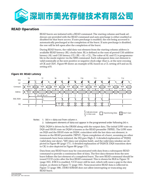
READ OperationREAD bursts are initiated with a READ command. The starting column and bank ad-dresses are provided with the READ command and auto precharge is either enabled or disabled for that burst access. If auto precharge is enabled, the row being accessed is automatically precharged at the completion of the burst. If auto precharge is disabled,the row will be left open after the completion of the burst.During READ bursts, the valid data-out element from the starting column address is available READ latency (RL) clocks later. RL is defined as the sum of posted CAS additive latency (AL) and CAS latency (CL) (RL = AL + CL). The value of AL and CL is programma-ble in the mode register via the MRS command. Each subsequent data-out element is valid nominally at the next positive or negative clock edge (that is, at the next crossing of CK and CK#). Figure 69 shows an example of RL based on a CL setting of 8 and an AL setting of 0.Figure 69: READ LatencyCKCK#CommandAddressDQDQS, DQS#Don’t CareTransitioning Data Indicates break in time scaleNotes:1.DO n = data-out from column n .2.Subsequent elements of data-out appear in the programmed order following DO n .DQS, DQS# is driven by the DRAM along with the output data. The initial LOW state on DQS and HIGH state on DQS# is known as the READ preamble (t RPRE). The LOW state on DQS and the HIGH state on DQS#, coincident with the last data-out element, isknown as the READ postamble (t RPST). Upon completion of a burst, assuming no other commands have been initiated, the DQ goes High-Z. A detailed explanation of t DQSQ (valid data-out skew), t QH (data-out window hold), and the valid data window are de-picted in Figure 80 (page 171). A detailed explanation of t DQSCK (DQS transition skew to CK) is also depicted in Figure 80 (page 171).Data from any READ burst may be concatenated with data from a subsequent READ command to provide a continuous flow of data. The first data element from the new burst follows the last element of a completed burst. The new READ command should be issued t CCD cycles after the first READ command. This is shown for BL8 in Figure 70(page 165). If BC4 is enabled, t CCD must still be met, which will cause a gap in the data output, as shown in Figure 71 (page 165). Nonconsecutive READ data is reflected in Figure 72 (page 166). DDR3 SDRAM does not allow interrupting or truncating any READ burst.Figure 100: Precharge Power-Down (Slow-Exit Mode) Entry and ExitCKCK#CommandCKEEnter power-downmode Exit power-downmodeDon’t CareIndicates break in time scaleNotes:1.Any valid command not requiring a locked DLL.2.Any valid command requiring a locked DLL.Figure 101: Power-Down Entry After READ or READ with Auto Precharge (RDAP)Don’t CareTransitioning Data CKCK#Command DQ BL8DQ BC4DQS, DQS#Address CKEPower-down or self refresh entryIndicates break in time scaleFigure 102: Power-Down Entry After WRITECKCK#Command DQ BL8DQ BC4DQS, DQS#AddressCKEself refresh entry1Don’t CareTransitioning Data Indicates break in time scaleNote:1.CKE can go LOW 2t CK earlier if BC4MRS.Figure 103: Power-Down Entry After WRITE with Auto Precharge (WRAP)Don’t CareTransitioning Data CKCK#CommandDQ BL8DQ BC4DQS, DQS#Address A10CKEPower-down or self refresh entry 2Start internal precharge Indicates break in time scaleNotes:1.t WR is programmed through MR0[11:9] and represents t WRmin (ns)/t CK rounded up tothe next integer t CK.2.CKE can go LOW 2t CK earlier if BC4MRS.Figure 104: REFRESH to Power-Down EntryCKCK#CommandCKET0T1T2T3Ta0Ta1Ta2Tb0Don’t CareIndicates break in time scaleNote:1.After CKE goes HIGH during t RFC, CKE must remain HIGH until t RFC is satisfied.Figure 105: ACTIVATE to Power-Down EntryCKCK#Command Address CKET0T1T2T3T4T5T6T7Figure 108: Power-Down Exit to Refresh to Power-Down EntryCKCK#CKET0T1T2T3T4Ta0Ta1Tb0Command。

Data SheetADuM1410/ADuM1411/ADuM1412FEATURESLow power operation 5 V operation1.3 mA per channel maximum at 0 Mbps to 2 Mbps 4.0 mA per channel maximum at 10 Mbps 3 V operation0.8 mA per channel maximum at 0 Mbps to 2 Mbps 1.8 mA per channel maximum at 10 Mbps Bidirectional communication 3 V/5 V level translationHigh temperature operation: 105°C Up to 10 Mbps data rate (NRZ)Programmable default output stateHigh common-mode transient immunity: >25 kV/µs 16-lead, RoHS compliant, SOIC wide body package Safety and regulatory approvalsUL recognition: 3750 V rms for 1 minute per UL 1577 CSA Component Acceptance Notice 5A VDE certificate of conformityDIN V VDE V 0884-10 (VDE V 0884-10): 2006-12 V IORM = 560 V peakTÜV approval: IEC/EN 60950-1V GND V V V V GND DD22OA OB OC OD2206580-001Figure 1. ADuM1410V GND V V V V CTRL GND DD22OA OB OC ID2206580-002Figure 2. ADuM1411V GND V V V V CTRL GNDDD22OA OB IC ID 2206580-003APPLICATIONSGeneral-purpose multichannel isolation SPI interface/data converter isolation RS-232/RS-422/RS-485 transceivers Industrial field bus isolationGENERAL DESCRIPTIONThe ADuM1410/ADuM1411/ADuM14121 are four-channel digital isolators based on Analog Devices, Inc., i Coupler® technology. Combining high speed CMOS and monolithic air core transformer technologies, these isolation components provide outstanding performance characteristics superior to alternatives such as optocoupler devices.By avoiding the use of LEDs and photodiodes, i Coupler devices remove the design difficulties commonly associated with opto-couplers. The usual concerns that arise with optocouplers, such as uncertain current transfer ratios, nonlinear transfer functions, and temperature and lifetime effects, are eliminated with the simple i Coupler digital interfaces and stable performance characteristics. The need for external drivers and other discrete components is eliminated with these i Coupler products. Furthermore, i Coupler1Protected by U.S. Patents 5,952,849; 6,873,065; 6,903,578; and 7,075,329.Figure 3. ADuM1412devices consume one-tenth to one-sixth the power of optocou-plers at comparable signal data rates.The ADuM1410/ADuM1411/ADuM1412 isolators provide four independent isolation channels in a variety of channel configu-rations and data rates (see the Ordering Guide) up to 10 Mbps. All models operate with the supply voltage on either side ranging from 2.7 V to 5.5 V , providing compatibility with lower voltage systems as well as enabling voltage translation functionality across the isolation barrier. All products also have a default output control pin. This allows the user to define the logic state the outputs are to adopt in the absence of the input power. Unlike other optocoupler alternatives, the ADuM1410/ADuM1411/ ADuM1412 isolators have a patented refresh feature that ensures dc correctness in the absence of input logic transitions and during power-up/power-down conditions.Data Sheet ADuM1410/ADuM1411/ADuM1412 SPECIFICATIONSELECTRICAL CHARACTERISTICS—5 V OPERATION4.5 V ≤ V DD1 ≤5.5 V, 4.5 V ≤ V DD2 ≤ 5.5 V; all minimum/maximum specifications apply over the entire recommended operation range, unless otherwise noted; all typical specifications are at T A = 25°C, V DD1 = V DD2 = 5 V. All voltages are relative to their respective ground. Table 1.Parameter Symbol Min Typ Max Unit Test Conditions/CommentsDC SPECIFICATIONSInput Supply Current per Channel,QuiescentI DDI (Q)0.50 0.73 mAOutput Supply Current per Channel,QuiescentI DDO (Q)0.38 0.53 mAADuM1410, Total Supply Current,Four Channels1DC to 2 MbpsV DD1 Supply Current I DD1 (Q) 2.4 3.2 mA DC to 1 MHz logic signal frequency V DD2 Supply Current I DD2 (Q) 1.2 1.6 mA DC to 1 MHz logic signal frequency10 Mbps (BRWZ Version Only)V DD1 Supply Current I DD1 (10)8.8 12 mA 5 MHz logic signal frequency V DD2 Supply Current I DD2 (10) 2.8 4.0 mA 5 MHz logic signal frequency ADuM1411, Total Supply Current,Four Channels1DC to 2 MbpsV DD1 Supply Current I DD1 (Q) 2.2 2.8 mA DC to 1 MHz logic signal frequency V DD2 Supply Current I DD2 (Q) 1.8 2.4 mA DC to 1 MHz logic signal frequency10 Mbps (BRWZ Version Only)V DD1 Supply Current I DD1 (10) 5.4 7.6 mA 5 MHz logic signal frequency V DD2 Supply Current I DD2 (10) 3.8 5.3 mA 5 MHz logic signal frequency ADuM1412, Total Supply Current,Four Channels1DC to 2 MbpsV DD1 or V DD2 Supply Current I DD1 (Q), I DD2(Q)2.0 2.6 mA DC to 1 MHz logic signal frequency10 Mbps (BRWZ Version Only)V DD1 or V DD2 Supply Current I DD1 (10), I DD2 (10) 4.6 6.5 mA 5 MHz logic signal frequencyAll ModelsInput Currents I IA, I IB, I IC,I ID, I CTRL1,I CTRL2, I DISABLE −10 +0.01 +10µA 0 V ≤ V IA, V IB, V IC, V ID ≤ V DD1 or V DD2,0 V ≤ V CTRL1, V CTRL2 ≤ V DD1 or V DD2,0 V ≤ V DISABLE ≤ V DD1Logic High Input Threshold V IH 2.0 V Logic Low Input Threshold V IL 0.8 VLogic High Output Voltages V OAH, V OBH,V OCH, V ODH (V DD1 or V DD2) − 0.1 5.0 V I Ox = −20 µA, V Ix = V IxH (V DD1 or V DD2) − 0.4 4.8 V I Ox = −4 mA, V Ix = V IxHLogic Low Output Voltages V OAL, V OBL,V OCL, V ODL0.0 0.1 V I Ox = 20 µA, V Ix = V IxL0.04 0.1 V I Ox = 400 µA, V Ix = V IxL0.2 0.4 V I Ox = 4 mA, V Ix = V IxL Rev. M | Page of 22ADuM1410/ADuM1411/ADuM1412 Data Sheet Parameter Symbol Min Typ Max Unit Test Conditions/Comments SWITCHING SPECIFICATIONSADuM1410ARWZ/ADuM1411ARWZ/ADuM1412ARWZMinimum Pulse Width2PW 1000 ns C L = 15 pF, CMOS signal levels Maximum Data Rate3 1 Mbps C L = 15 pF, CMOS signal levels Propagation Delay4t PHL, t PLH20 65 100 ns C L = 15 pF, CMOS signal levels Pulse Width Distortion, |t PLH − t PHL|4 PWD 40 ns C L = 15 pF, CMOS signal levels Propagation Delay Skew5t PSK50 ns C L = 15 pF, CMOS signal levels Channel-to-Channel Matching6t PSKCD/OD50 ns C L = 15 pF, CMOS signal levels ADuM1410BRWZ/ADuM1411BRWZ/ADuM1412BRWZMinimum Pulse Width2PW 100 ns C L = 15 pF, CMOS signal levels Maximum Data Rate310 Mbps C L = 15 pF, CMOS signal levels Propagation Delay4t PHL, t PLH20 30 50 ns C L = 15 pF, CMOS signal levels Pulse Width Distortion, |t PLH − t PHL|4 PWD 5 ns C L = 15 pF, CMOS signal levels Change vs. Temperature 5 ps/°C C L = 15 pF, CMOS signal levels Propagation Delay Skew5t PSK30 ns C L = 15 pF, CMOS signal levels Channel-to-Channel Matching,Codirectional Channels6t PSKCD 5 ns C L = 15 pF, CMOS signal levelsChannel-to-Channel Matching,Opposing-Directional Channels6t PSKOD 6 ns C L = 15 pF, CMOS signal levelsAll ModelsOutput Rise/Fall Time (10% to 90%) t R/t F 2.5 ns C L = 15 pF, CMOS signal levelsCommon-Mode Transient Immunity at Logic High Output7|CM H| 25 35 kV/µs V Ix = V DD1 or V DD2, V CM = 1000 V,transient magnitude = 800 VCommon-Mode Transient Immunity at Logic Low Output7 |CM L| 25 35 kV/µs V Ix = 0 V, V CM = 1000 V,transient magnitude = 800 VRefresh Rate f r 1.2 MbpsInput Enable Time8t ENABLE 2.0 µs V IA, V IB, V IC, V ID = 0 V or V DD1 Input Disable Time8t DISABLE 5.0 µs V IA, V IB, V IC, V ID = 0 V or V DD1Input Dynamic Supply Current per Channel9I DDI (D)0.12 mA/MbpsOutput Dynamic Supply Current per Channel9I DDO (D)0.04 mA/Mbps1 The supply current values for all four channels are combined when running at identical data rates. Output supply current values are specified with no output load present. The supply current associated with an individual channel operating at a given data rate can be calculated as described in the Power Consumption section. See Figure 8 through Figure 10 for information on per-channel supply current as a function of data rate for unloaded and loaded conditions. See Figure 11 through Figure 15 for total V DD1 and V DD2 supply currents as a function of data rate for ADuM1410/ADuM1411/ADuM1412 channel configurations.2 The minimum pulse width is the shortest pulse width at which the specified pulse width distortion is guaranteed.3 The maximum data rate is the fastest data rate at which the specified pulse width distortion is guaranteed.4 t PHL propagation delay is measured from the 50% level of the falling edge of the V Ix signal to the 50% level of the falling edge of the V Ox signal. t PLH propagation delay is measured from the 50% level of the rising edge of the V Ix signal to the 50% level of the rising edge of the V Ox signal.5 t PSK is the magnitude of the worst-case difference in t PHL or t PLH that is measured between units at the same operating temperature, supply voltages, and output load within the recommended operating conditions.6 Codirectional channel-to-channel matching is the absolute value of the difference in propagation delays between any two channels with inputs on the same side of the isolation barrier. Opposing-directional channel-to-channel matching is the absolute value of the difference in propagation delays between any two channels with inputs on opposing sides of the isolation barrier.7 |CM H| is the maximum common-mode voltage slew rate that can be sustained while maintaining V O > 0.8 V DD2. |CM L| is the maximum common-mode voltage slew rate that can be sustained while maintaining V O < 0.8 V. The common-mode voltage slew rates apply to both rising and falling common-mode voltage edges. The transient magnitude is the range over which the common mode is slewed.8 Input enable time is the duration from when V DISABLE is set low until the output states are guaranteed to match the input states in the absence of any input data logic transitions. If an input data logic transition within a given channel does occur within this time interval, the output of that channel reaches the correct state within the much shorter duration as determined by the propagation delay specifications within this data sheet. Input disable time is the duration from when V DISABLE is set high until the output states are guaranteed to reach their programmed output levels, as determined by the CTRL2 logic state (see Table 14).9 Dynamic supply current is the incremental amount of supply current required for a 1 Mbps increase in signal data rate. See Figure 8 through Figure 10 for information on per-channel supply current for unloaded and loaded conditions. See the Power Consumption section for guidance on calculating the per-channel supply current for a given data rate.Rev. M | Page of 22Data Sheet ADuM1410/ADuM1411/ADuM1412ELECTRICAL CHARACTERISTICS—3 V OPERATION2.7 V ≤ V DD1 ≤3.6 V, 2.7 V ≤ V DD2 ≤ 3.6 V; all minimum/maximum specifications apply over the entire recommended operation range, unless otherwise noted; all typical specifications are at T A = 25°C, V DD1 = V DD2 = 3.0 V. All voltages are relative to their respective ground. Table 2.Parameter Symbol Min Typ Max Unit Test Conditions/CommentsDC SPECIFICATIONSInput Supply Current per Channel,QuiescentI DDI (Q)0.25 0.38 mAOutput Supply Current per Channel,QuiescentI DDO (Q)0.19 0.33 mAADuM1410, Total Supply Current,Four Channels1DC to 2 MbpsV DD1 Supply Current I DD1 (Q) 1.2 1.6 mA DC to 1 MHz logic signalfrequency V DD2 Supply Current I DD2 (Q)0.8 1.0 mA DC to 1 MHz logic signalfrequency10 Mbps (BRWZ Version Only)V DD1 Supply Current I DD1 (10) 4.5 6.5 mA 5 MHz logic signal frequency V DD2 Supply Current I DD2 (10) 1.4 1.8 mA 5 MHz logic signal frequency ADuM1411, Total Supply Current,Four Channels1DC to 2 MbpsV DD1 Supply Current I DD1 (Q) 1.0 1.9 mA DC to 1 MHz logic signal frequency V DD2 Supply Current I DD2 (Q)0.9 1.7 mA DC to 1 MHz logic signal frequency10 Mbps (BRWZ Version Only)V DD1 Supply Current I DD1 (10) 3.1 4.5 mA 5 MHz logic signal frequency V DD2 Supply Current I DD2 (10) 2.1 3.0 mA 5 MHz logic signal frequency ADuM1412, Total Supply Current,Four Channels1DC to 2 MbpsV DD1 or V DD2 Supply Current I DD1 (Q), I DD2 (Q) 1.0 1.8 mA DC to 1 MHz logic signal frequency10 Mbps (BRWZ Version Only)V DD1 or V DD2 Supply Current I DD1 (10), I DD2 (10) 2.6 3.8 mA 5 MHz logic signal frequencyAll ModelsInput Currents I IA, I IB, I IC, I ID,I CTRL1,I CTRL2, I DISABLE −10 +0.01 +10µA 0 V ≤ V IA, V IB, V IC, V ID ≤ V DD1 or V DD2,0 V ≤ V CTRL1, V CTRL2 ≤ V DD1 or V DD2,0 V ≤ V DISABLE ≤ V DD1Logic High Input Threshold V IH 1.6 V Logic Low Input Threshold V IL 0.4 VLogic High Output Voltages V OAH, V OBH,V OCH, V ODH (V DD1 or V DD2) − 0.1 3.0 V I Ox = −20 µA, V Ix = V IxH (V DD1 or V DD2) − 0.4 2.8 V I Ox = −4 mA, V Ix = V IxHLogic Low Output Voltages V OAL, V OBL,V OCL, V ODL0.0 0.1 V I Ox = 20 µA, V Ix = V IxL0.04 0.1 V I Ox = 400 µA, V Ix = V IxL0.2 0.4 V I Ox = 4 mA, V Ix = V IxL Rev. M | Page of 22ADuM1410/ADuM1411/ADuM1412 Data Sheet。

6.5Write ProtectionApplications that use non-volatile memory must take into consideration the possibility of noise and other adverse system conditions that may compromise data integrity. To address this concern, the W25Q32JV provides several means to protect the data from inadvertent writes.Write Protect Features∙Device resets when VCC is below threshold∙Time delay write disable after Power-up∙Write enable/disable instructions and automatic write disable after erase or program∙Software and Hardware (/WP pin) write protection using Status Registers∙Additional Individual Block/Sector Locks for array protection∙Write Protection using Power-down instruction∙Lock Down write protection for Status Register until the next power-up∙One Time Program (OTP) write protection for array and Security Registers using Status Register* *Note:This feature is available upon special order. Please contact Winbond for details.Upon power-up or at power-down, the W25Q32JV will maintain a reset condition while VCC is below the threshold value of V WI, (See Power-up Timing and Voltage Levels and Figure 43). While reset, all operations are disabled and no instructions are recognized. During power-up and after the VCC voltage exceeds V WI, all program and erase related instructions are further disabled for a time delay of t PUW. This includes the Write Enable, Page Program, Sector Erase, Block Erase, Chip Erase and the Write Status Register instructions. Note that the chip select pin (/CS) must track the VCC supply level at power-up until the VCC-min level and t VSL time delay is reached, and it must also track the VCC supply level at power-down to prevent adverse command sequence. If needed a pull-up resister on /CS can be used to accomplish this.After power-up the device is automatically placed in a write-disabled state with the Status Register Write Enable Latch (WEL) set to a 0. A Write Enable instruction must be issued before a Page Program, Sector Erase, Block Erase, Chip Erase or Write Status Register instruction will be accepted. After completing a program, erase or write instruction the Write Enable Latch (WEL) is automatically cleared to a write-disabled state of 0.Software controlled write protection is facilitated using the Write Status Register instruction and setting the Status Register Protect (SRP, SRL) and Block Protect (CMP, TB, BP[2:0]) bits. These settings allow a portion or the entire memory array to be configured as read only. Used in conjunction with the Write Protect (/WP) pin, changes to the Status Register can be enabled or disabled under hardware control. See Status Register section for further information. Additionally, the Power-down instruction offers an extra level of write protection as all instructions are ignored except for the Release Power-down instruction.The W25Q32JV also provides another Write Protect method using the Individual Block Locks. Each 64KB block (except the top and bottom blocks, total of 62 blocks) and each 4KB sector within the top/bottom blocks (total of 32 sectors) are equipped with an Individual Block Lock bit. When the lock bit is 0, the corresponding sector or block can be erased or programmed; when the lock bit is set to 1, Erase or Program commands issued to the corresponding sector or block will be ignored. When the device is powered on, all Individual Block Lock bits will be 1, so the entire memory array is protected from Erase/Program. An “Individual Block Unlock (39h)” instruction must be issued to unlock any specific sector or block.The WPS bit in Status Register-3 is used to decide which Write Protect scheme should be used. When WPS=0 (factory default), the device will only utilize CMP, SEC, TB, BP[2:0] bits to protect specific areas of the array; when WPS=1, the device will utilize the Individual Block Locks for write protection.Figure 4c. Status Register-3Write Protect Selection (WPS) –Volatile/Non-Volatile WritableThe WPS bit is used to select which Write Protect scheme should be used. When WPS=0, the device will use the combination of CMP, SEC, TB, BP[2:0] bits to protect a specific area of the memory array. When WPS=1, the device will utilize the Individual Block Locks to protect any individual sector or blocks. Thedefault value for all Individual Block Lock bits is 1 upon device power on or after reset.Output Driver Strength (DRV1, DRV0) –Volatile/Non-Volatile WritableThe DRV1 & DRV0 bits are used to determine the output driver strength for the Read operations.Reserved Bits –Non FunctionalThere are a few reserved Status Register bits that may be read out as a “0” or “1”. It is recommended to ignore the values of those bits. During a “Write Status Register” instruction, the Reserved Bits can be written as “0”, but there will not be any effects.Status Register Memory Protection (WPS = 0, CMP = 0)Notes:1.X = don’t care2.L = Lower; U = Upper3.If any Erase or Program command specifies a memory region that contains protected data portion, this commandwill be ignored.Write Status Register-1 (01h), Status Register-2 (31h) & Status Register-3 (11h)The Write Status Register instruction allows the Status Registers to be written. The writable Status Register bits include: SEC, TB, BP[2:0] in Status Register-1; CMP, LB[3:1], QE, SRL in Status Register-2; DRV1, DRV0, WPS in Status Register-3. All other Status Register bit locations are read-only and will not be affected by the Write Status Register instruction. LB[3:1] are non-volatile OTP bits, once it is set to 1, it cannot be cleared to 0.To write non-volatile Status Register bits, a standard Write Enable (06h) instruction must previously have been executed for the device to accept the Write Status Register instruction (Status Register bit WEL must equal 1). Once write enabled, the instruction is entered by driving /CS low, sending the instruction code “01h/31h/11h”, and then writing the status register data byte as illustrated in Figure 9a.To write volatile Status Register bits, a Write Enable for Volatile Status Register (50h) instruction must have been executed prior to the Write Status Register instruction (Status Register bit WEL remains 0). However, SRL and LB[3:1] cannot be changed from “1” to “0” because of the OTP protection for these bits. Upon power off or the execution of a Software/Hardware Reset, the volatile Status Register bit values will be lost, and the non-volatile Status Register bit values will be restored.During non-volatile Status Register write operation (06h combined with 01h/31h/11h), after /CS is driven high, the self-timed Write Status Register cycle will commence for a time duration of t W(See AC Characteristics). While the Write Status Register cycle is in progress, the Read Status Register instruction may still be accessed to check the status of the BUSY bit. The BUSY bit is a 1 during the Write Status Register cycle and a 0 when the cycle is finished and ready to accept other instructions again. After the Write Status Register cycle has finished, the Write Enable Latch (WEL) bit in the Status Register will be cleared to 0.During volatile Status Register write operation (50h combined with 01h/31h/11h), after /CS is driven high, the Status Register bits will be refreshed to the new values within the time period of t SHSL2(See AC Characteristics). BUSY bit will remain 0 during the Status Register bit refresh period.Refer to section 7.1 for Status Register descriptions.Figure 9a. Write Status Register-1/2/3 Instruction。

ADM485FUNCTIONAL BLOCK DIAGRAMCC 00078-001FEATURESMeets EIA RS-485 standard 5 Mbps data rateSingle 5 V supply–7 V to +12 V bus common-mode range High speed, low power BiCMOS Thermal shutdown protection Short-circuit protectionDriver propagation delay: 10 ns typical Receiver propagation delay: 15 ns typical High-Z outputs with power off Superior upgrade for LTC485APPLICATIONSLow power RS-485 systems DTE/DCE interface Packet switchingLocal area networks (LNAs) Data concentration Data multiplexersIntegrated services digital network (ISDN)GENERAL DESCRIPTIONThe ADM485 is a differential line transceiver suitable for high speed bidirectional data communication on multipoint bus transmission lines. It is designed for balanced data transmission and complies with EIA standards RS-485 and RS-422. The part contains a differential line driver and a differential line receiver. Both the driver and the receiver can be enabled independently. When disabled, the outputs are three-stated.The ADM485 operates from a single 5 V power supply. Excessive power dissipation caused by bus contention or by output shorting is prevented by a thermal shutdown circuit. If during fault conditions, a significant temperature increase is detected in the internal driver circuitry, this feature forces the driver output into a high impedance state.Up to 32 transceivers can be connected simultaneously on a bus, but only one driver should be enabled at any time. It is important, therefore, that the remaining disabled drivers do not load the bus. To ensure this, the ADM485 driver features high output impedance when disabled and when powered down, which minimizes the loading effect when the transceiver is not being used. The high impedance driver output is maintained over the common-mode voltage range of −7 V to +12 V .Figure 1.The receiver contains a fail-safe feature that results in a logic high output state if the inputs are unconnected (floating). The ADM485 is fabricated on BiCMOS, an advanced mixed technology process combining low power CMOS with fast switching bipolar technology. All inputs and outputs contain protection against ESD; all driver outputs feature high source and sink current capability. An epitaxial layer is used to guard against latch-up.The ADM485 features extremely fast switching speeds. Minimal driver propagation delays permit transmission at data rates up to 5 Mbps while low skew minimizes EMI interference. The part is fully specified over the commercial and industrial temperature range and is available in 8-lead PDIP , 8-lead SOIC, and small footprint, 8-lead MSOP packages.ADM485Rev. F | Page 2 of 16ADM485SPECIFICATIONSV CC = 5 V ± 5%, all specifications T MIN to T MAX, unless otherwise noted.Rev. F | Page 3 of 16ADM485TIMING SPECIFICATIONSV CC = 5 V ± 5%, all specifications T MIN to T MAX, unless otherwise noted.1 Guaranteed by characterization.Rev. F | Page 4 of 16ADM485Rev. F | Page 5 of 16ABSOLUTE MAXIMUM RATINGST A = 25°C, unless otherwise noted.Stresses above those listed under Absolute Maximum Ratings may cause permanent damage to the device. This is a stress rating only; functional operation of the device at these or any other conditions above those indicated in the operationalsection of this specification is not implied. Exposure to absolute maximum rating conditions for extended periods may affect device reliability.Table 4. TransmittingInputsOutputsDE DIB A 1 1 0 1 1 0 1 0 0X 1Z 2Z 21 X = don’t care.2Z = high impedance.1 X = don’t care.2Z = high impedance.ESD CAUTION。


__________________________________________Typical Operating Characteristics(V CC = +3.3V, 235kbps data rate, 0.1µF capacitors, all transmitters loaded with 3k Ω, T A = +25°C, unless otherwise noted.)TIMING CHARACTERISTICS—MAX3237(V CC = +3.0V to +5.5V, C1–C4 = 0.1µF (Note 2), T A = T MIN to T MAX , unless otherwise noted. Typical values are at T A = +25°C.)Note 2:MAX3222/MAX3232/MAX3241: C1–C4 = 0.1µF tested at 3.3V ±10%; C1 = 0.047µF, C2–C4 = 0.33µF tested at 5.0V ±10%.MAX3237: C1–C4 = 0.1µF tested at 3.3V ±5%; C1–C4 = 0.22µF tested at 3.3V ±10%; C1 = 0.047µF, C2–C4 = 0.33µF tested at 5.0V ±10%.Note 3:Transmitter input hysteresis is typically 250mV.-6-5-4-3-2-101234560MAX3222/MAX3232TRANSMITTER OUTPUT VOLTAGEvs. LOAD CAPACITANCELOAD CAPACITANCE (pF)T R A N S M I T T E R O U T P U T V O L T A G E (V )20003000100040005000246810121416182022150MAX3222/MAX3232SLEW RATEvs. LOAD CAPACITANCELOAD CAPACITANCE (pF)S L E W R A T E (V /μs )20003000100040005000510152025303540MAX3222/MAX3232SUPPLY CURRENT vs. LOAD CAPACITANCEWHEN TRANSMITTING DATALOAD CAPACITANCE (pF)S U P P L Y C U R R E N T (m A )20003000100040005000MAX3222/MAX3232/MAX3237/MAX32413.0V to 5.5V, Low-Power, up to 1Mbps, True RS-232 Transceivers Using Four 0.1µF External CapacitorsFigure 4a. MAX3241 Transmitter Output Voltage vs. Load Current per Transmitter3.0V to 5.5V , Low-Power, up to 1Mbps, True RS-232Transceivers Using Four 0.1µF External CapacitorsMAX3222/MAX3232/MAX3237/MAX3241CC = 3.3V5μs/divFigure 5. Loopback Test CircuitHigh Data RatesThe MAX3222/MAX3232/MAX3241 maintain the RS-232±5.0V minimum transmitter output voltage even at high data rates. Figure 5 shows a transmitter loopb ack test circuit. Figure 6 shows a loopb ack test result at 120kbps, and Figure 7 shows the same test at 235kbps. For Figure 6, all transmitters were driven simultaneously at 120kb ps into RS-232 loads in parallel with 1000pF. For Figure 7, a single transmitter was driven at 235kbps, and all transmitters were loaded with an RS-232 receiver in parallel with 1000pF.The MAX3237 maintains the RS-232 ±5.0V minimum transmitter output voltage at data rates up to 1Mb ps. Figure 8 shows a loopb ack test result at 1Mb ps with MBAUD = V CC . For Figure 8, all transmitters were loaded with an RS-232 receiver in parallel with 250pF.fdzfdfbbFigure 6. MAX3241 Loopback Test Result at 120kbpsCC = 3.3V2μs/divFigure 7. MAX3241 Loopback Test Result at 235kbps0V +5V 0V -5V +5V 0VT_INT_OUT = R_IN 5k R_OUT 150pF200ns/divCC = 3.3VFigure 8. MAX3237 Loopback Test Result at 1000kbps (MBAUD = V CC )___________________Chip Topography___________________Chip InformationT1INT2IN 0.087"(2.209mm)R2OUTR2IN T2OUT R1OUTR1INT1OUTV CCV+C1+ENC1-C2+C2-V-GNDTRANSISTOR COUNT: 339SUBSTRATE CONNECTED TO GNDMAX3222/MAX3232/MAX3237/MAX3241 3.0V to 5.5V, Low-Power, up to 1Mbps, True RS-232Transceivers Using Four 0.1µF External Capacitors。

ADG3304Data Sheet Rev. E | Page 16 of 21TERMINOLOGYV IHALogic input high voltage at Pin A1 to Pin A4. V ILALogic input low voltage at Pin A1 to Pin A4. V OHA Logic output high voltage at Pin A1 to Pin A4. V OLA Logic output low voltage at Pin A1 to Pin A4. C A Capacitance measured at Pin A1 to Pin A4 (EN = 0). I LA, Hi-ZLeakage current at Pin A1 to Pin A4 when EN = 0 (high impedance state at Pin A1 to Pin A4).V IHYLogic input high voltage at Pin Y1 to Pin Y4. V ILYLogic input low voltage at Pin Y1 to Pin Y4. V OHY Logic output high voltage at Pin Y1 to Pin Y4. V OLY Logic output low voltage at Pin Y1 to Pin Y4. C Y Capacitance measured at Pin Y1 to Pin Y4 (EN = 0). I LY , Hi-ZLeakage current at Pin Y1 to Pin Y4 when EN = 0 (high impedance state at Pin Y1 to Pin Y4).V IHENLogic input high voltage at the EN pin.V ILENLogic input low voltage at the EN pin.C ENCapacitance measured at EN pin.I LENEnable (EN) pin leakage current.t ENThree-state enable time for Pin A1 to Pin A4 and Pin Y1 to Pin Y4.t P , A→YPropagation delay when translating logic levels in the A→Y direction.t R, A→YRise time when translating logic levels in the A→Y direction. T F, A→Y Fall time when translating logic levels in the A→Y direction. D MAX, A→Y Guaranteed data rate when translating logic levels in the A→Y direction under the driving and loading conditions specified in Table 1. T S KEW , A→Y Difference between propagation delays on any two channels when translating logic levels in the A→Y direction. t PPSKEW , A→Y Difference in propagation delay between any one channel and the same channel on a different part (under same driving/ loading conditions) when translating in the A→Y direction. t P , Y→A Propagation delay when translating logic levels in the Y→A direction. t R, Y→A Rise time when translating logic levels in the Y→A direction. t F, Y→A Fall time when translating logic levels in the Y→A direction. D MAX, Y→A Guaranteed data rate when translating logic levels in the Y→A direction under the driving and loading conditions specified in Table 1. t S KEW , Y→A Difference between propagation delays on any two channels when translating logic levels in the Y→A direction. t PPSKEW , Y→A Difference in propagation delay between any one channel and the same channel on a different part (under the same driving/ loading conditions) when translating in the Y→A direction. V CCA V CCA supply voltage. V CCY V CCY supply voltage. I CCA V CCA supply current. I CCY V CCY supply current. I Hi-Z, A V CCA supply current during three-state mode (EN = 0). I Hi-Z, Y V CCY supply current during three-state mode (EN = 0).Data SheetADG3304 Rev. E | Page 17 of 21THEORY OF OPERATIONThe ADG3304 level translator allows the level shifting necessary for data transfer in a system where multiple supply voltages are used. The device requires two supplies, V CCA and V CCY (V CCA ≤ V CCY ). These supplies set the logic levels on each side of the device. When driving the A pins, the device translates the V CCA -compatible logic levels to V CCY -compatible logic levels available at the Y pins. Similarly, because the device is capable of bidirectional translation, when driving the Y pins, the V CCY -compatible logic levels are translated to V CCA -compatible logic levels available at the A pins. When EN = 0, Pin A1 to Pin A4 and Pin Y1 to Pin Y4 are three-stated. When EN is driven high, the ADG3304 goes into normal operation mode and performs level translation. LEVEL TRANSLATOR ARCHITECTURE The ADG3304 consists of four bidirectional channels. Each channel can translate logic levels in either the A→Y or the Y→A direction. It uses a one-shot accelerator architecture, which ensures excellent switching characteristics. Figure 39 shows a simplified block diagram of a bidirectional channel.Y 04860-053Figure 39. Simplified Block Diagram of an ADG3304 Channel The logic level translation in the A→Y direction is performed using a level translator (U1) and an inverter (U2), while the translation in the Y→A direction is performed using Inverter U3 and Inverter U4. The one-shot generator detects a rising or falling edge present on either the A side or the Y side of the channel. It sends a short pulse that turns on the PMOS transistors (T1 to T2) for a rising edge, or the NMOS transistors (T3 to T4) for a falling edge. This charges/discharges the capacitive load faster, which results in faster rise and fall times.The inputs of the unused channels (A or Y) should be tied to their corresponding V CC rail (V CCA or V CCY ) or to GND. INPUT DRIVING REQUIREMENTS To ensure correct operation of the ADG3304, the circuit that drives the input of the ADG3304 channels should have an output impedance of less than or equal to 150 Ω and a minimum peak current driving capability of 36 mA. OUTPUT LOAD REQUIREMENTS The ADG3304 level translator is designed to drive CMOS-compatible loads. If current-driving capability is required, it is recommended to use buffers between the ADG3304 outputs and the load. ENABLE OPERATIONThe ADG3304 provides three-state operation at the A and Y I/O pins by using the enable pin (EN), as shown in Table 5. Table 5. Truth TableENY I/O Pins A I/O Pins 0Hi-Z 1 Hi-Z 1 1Normal operation 2Normal operation 21High impedance state.2 In normal operation, the ADG3304 performs level translation.While EN = 0, the ADG3304 enters into three-state mode. In this mode, the current consumption from both the V CCA and V CCY supplies is reduced, allowing the user to save power, which is critical, especially on battery-operated systems. The EN input pin can be driven with either V CCA -compatible or V CCY -compatible logic levels.POWER SUPPLIESFor proper operation of the ADG3304, the voltage applied to the V CCA must be less than or equal to the voltage applied to V CCY . To meet this condition, the recommended power-up sequence is V CCY first and then V CCA . The ADG3304 operates properly only after both supply voltages reach their nominal values. It is not recommended to use the part in a system where, during power-up, V CCA can be greater than V CCY due to a significant increase in the current taken from the V CCA supply. For optimum performance, the V CCA pin and V CCY pin should be decoupled to GND as close as possible to the device.。

Integrated | 10Shutdown and Enable Control (MAX205E/MAX206E/MAX211E/MAX213E/MAX241E)In shutdown mode, the charge pumps are turned off,V+ is pulled down to V CC , V- is pulled to ground, and the transmitter outputs are disabled. This reduces sup-ply current typically to 1µA (15µA for the MAX213E).The time required to exit shutdown is under 1ms, asshown in Figure 5.Receivers All MAX213E receivers, except R4 and R5, are put into a high-impedance state in shutdown mode (see Tables 1a and 1b). The MAX213E’s R4 and R5 receivers still function in shutdown mode. These two awake-in-shut-down receivers can monitor external activity while main-taining minimal power consumption.The enable control is used to put the receiver outputs into a high-impedance state, to allow wire-OR connection of two EIA/TIA-232E ports (or ports of different types) at the UART. It has no effect on the RS-232 drivers or the charge pumps.Note: The enable c ontrol pin is ac tive low for the MAX211E/MAX241E (EN ), but is ac tive high for theMAX213E (EN). The shutdown control pin is active highFigure 4. Charge-Pump DiagramWhen in low-power shutdown mode, the MAX205E/MAX206E/MAX211E/MAX213E/MAX241E driver outputsare turned off and draw only leakage currents—even ifthey are back-driven with voltages between 0V and12V. Below -0.5V in shutdown, the transmitter output isdiode-clamped to ground with a 1k Ω series imped-ance.RS-232 ReceiversThe receivers convert the RS-232 signals to CMOS-logicoutput levels. The guaranteed 0.8V and 2.4V receiverinput thresholds are significantly tighter than the ±3Vthresholds required by the EIA/TIA-232E specification.This allows the receiver inputs to respond to TTL/CMOS-logic levels, as well as RS-232 levels.The guaranteed 0.8V input low threshold ensures thatreceivers shorted to ground have a logic 1 output. The5k Ω input resistance to ground ensures that a receiverwith its input left open will also have a logic 1 output.Receiver inputs have approximately 0.5V hysteresis.This provides clean output transitions, even with slowrise/fall-time signals with moderate amounts of noiseand ringing.In shutdown, the MAX213E’s R4 and R5 receivers haveno hysteresis.找MEMORY 、二三极管上美光存储Integrated | 13MAX202E–MAX213E,MAX232E/MAX241E ±15kV ESD-Protected, 5V RS-232 Transceivers outputs. Therefore,after PC board assembly,theMachine Model is less relevant to I/O ports.Applications InformationCapacitor SelectionThe capacitor type used for C1–C4 is not critical forproper operation. The MAX202E, MAX206–MAX208E,MAX211E, and MAX213E require 0.1µF capacitors,and the MAX232E and MAX241E require 1µF capaci-tors, although in all cases capacitors up to 10µF canbe used without harm. Ceramic, aluminum-electrolytic,or tantalum capacitors are suggested for the 1µFcapacitors, and ceramic dielectrics are suggested forthe 0.1µF capacitors. When using the minimum recom-mended capacitor values, make sure the capacitancevalue does not degrade excessively as the operatingtemperature varies. If in doubt, use capacitors with alarger (e.g., 2x) nominal value. The capacitors’ effec-tive series resistance (ESR), which usually rises at lowtemperatures, influences the amount of ripple on V+and V-.Use larger capacitors (up to 10µF) to reduce the outputimpedance at V+ and V-. This can be useful when“stealing” power from V+ or from V-. The MAX203E andMAX205E have internal charge-pump capacitors.Bypass V CC to ground with at least 0.1µF. In applica-tions sensitive to power-supply noise generated by the charge pumps, decouple V CC to ground with a capaci-tor the same size as (or larger than) the charge-pump capacitors (C1–C4).V+ and V- as Power Supplies A small amount of power can be drawn from V+ and V-,although this will reduce both driver output swing and noise margins. Increasing the value of the charge-pump capacitors (up to 10µF ) helps maintain performance when power is drawn from V+ or V-.Driving Multiple Receivers Each transmitter is designed to drive a single receiver.Transmitters can be paralleled to drive multiple receivers.Driver Outputs when Exiting Shutdown The driver outputs display no ringing or undesirable transients as they come out of shutdown.High Data Rates These transceivers maintain the RS-232 ±5.0V mini-mum driver output voltages at data rates of over 120kbps. F or data rates above 120kbps, refer to the Transmitter Output Voltage vs. Load Capacitance graphs in the Typical Operating Characteristics .Communication at these high rates is easier if the capacitive loads on the transmitters are small; i.e.,short cables are best.Table 2. Summary of EIA/TIA-232E, V.28 Specifications PARAMETERCONDITIONS EIA/TIA-232E, V.28 SPECIFICA-TIONS 0 Level3k Ωto 7k Ωload +5V to +15V Data Rate 3k Ω≤R L ≤7k Ω, C L ≤2500pFUp to 20kbps +3V to +15V Instantaneous Slew Rate, Max 3k Ω≤R L ≤7k Ω, C L ≤2500pF 30V/µsDriver Output Short-Circuit Current, Max 100mATransition Rate on Driver Output V.281ms or 3% of the period Driver Output Resistance-2V < V OUT < +2V 300ΩEIA/TIA-232E4% of the period Driver Output Level, Max No load±25V Driver Output Voltage 3k Ωto 7k Ωload-5V to -15V 0 Level1 Level 1 Level Receiver Input Level ±25VReceiver Input Voltage -3V to -15V。

Table 54: Electrical Characteristics and AC Operating Conditions (Continued)Notes: 1.AC timing parameters are valid from specified T C MIN to T C MAX values.2.All voltages are referenced to V SS.3.Output timings are only valid for R ON34 output buffer selection.4.The unit t CK (AVG) represents the actual t CK (AVG) of the input clock under operation.The unit CK represents one clock cycle of the input clock, counting the actual clockedges.5.AC timing and I DD tests may use a V IL-to-V IH swing of up to 900mV in the test environ-ment, but input timing is still referenced to V REF (except t IS, t IH, t DS, and t DH use theAC/DC trip points and CK, CK# and DQS, DQS# use their crossing points). The minimumslew rate for the input signals used to test the device is 1 V/ns for single-ended inputsand 2 V/ns for differential inputs in the range between V IL(AC) and V IH(AC).6.All timings that use time-based values (ns, μs, ms) should use t CK (AVG) to determine thecorrect number of clocks (Table 54 (page 72) uses CK or t CK [AVG] interchangeably). Inthe case of noninteger results, all minimum limits are to be rounded up to the nearestwhole integer, and all maximum limits are to be rounded down to the nearest wholeinteger.7.Strobe or DQS diff refers to the DQS and DQS# differential crossing point when DQS isthe rising edge. Clock or CK refers to the CK and CK# differential crossing point whenCK is the rising edge.8.This output load is used for all AC timing (except ODT reference timing) and slew rates.The actual test load may be different. The output signal voltage reference point isV DDQ/2 for single-ended signals and the crossing point for differential signals (see Fig-ure 26 (page 64)).9.When operating in DLL disable mode, Micron does not warrant compliance with normalmode timings or functionality.Table 55: Electrical Characteristics and AC Operating Conditions for Speed ExtensionsTable 55: Electrical Characteristics and AC Operating Conditions for Speed Extensions (Continued)Table 55: Electrical Characteristics and AC Operating Conditions for Speed Extensions (Continued)Table 55: Electrical Characteristics and AC Operating Conditions for Speed Extensions (Continued)。

203TMS320C6745,TMS320C6747SPRS377F –SEPTEMBER 2008–REVISED JUNE 2014Submit Documentation FeedbackProduct Folder Links:TMS320C6745TMS320C6747Peripheral Information and Electrical SpecificationsCopyright ©2008–2014,Texas Instruments Incorporated 6.29Programmable Real-Time Unit Subsystem (PRUSS)The Programmable Real-Time Unit Subsystem (PRUSS)consists of•Two Programmable Real-Time Units (PRU0and PRU1)and their associated memories•An Interrupt Controller (INTC)for handling system interrupt events.The INTC also supports posting events back to the device level host CPU.•A Switched Central Resource (SCR)for connecting the various internal and external masters to the resources inside the PRUSS.The two PRUs can operate completely independently or in coordination with each other.The PRUs can also work in coordination with the device level host CPU.This is determined by the nature of the program which is loaded into the PRUs instruction memory.Several different signaling mechanisms are available between the two PRUs and the device level host CPU.The PRUs are optimized for performing embedded tasks that require manipulation of packed memory mapped data structures,handling of system events that have tight realtime constraints and interfacing with systems external to the device.The PRUSS comprises various distinct addressable regions.Externally the subsystem presents a single 64Kbyte range of addresses.The internal interconnect bus (also called switched central resource,or SCR)of the PRUSS decodes accesses for each of the individual regions.The PRUSS memory map is documented in Table 6-105and in Table 6-106.Note that these two memory maps are implemented inside the PRUSS and are local to the components of the PRUSS.Table 6-105.Programmable Real-Time Unit Subsystem (PRUSS)Local Instruction Space Memory MapBYTE ADDRESSPRU0PRU10x00000000-0x00000FFF PRU0Instruction RAM PRU1Instruction RAM(1)Note that PRU0accesses Data RAM 0at address 0x00000000,also PRU1accesses Data RAM 1at address 0x00000000.Data RAM0is intended to be the primary data memory for PRU0and Data RAM1is intended to be the primary data memory for PRU1.However for passing information between PRUs,each PRU can access the data ram of the ‘other’PRU through address 0x00002000.Table 6-106.Programmable Real-Time Unit Subsystem (PRUSS)Local Data Space Memory MapBYTE ADDRESSPRU0PRU10x00000000-0x000001FFData RAM 0(1)Data RAM 1(1)0x00000200-0x00001FFFReserved Reserved 0x00002000-0x000021FFData RAM 1(1)Data RAM 0(1)0x00002200-0x00003FFFReserved Reserved 0x00004000-0x00006FFFINTC Registers INTC Registers 0x00007000-0x000073FFPRU0Control Registers PRU0Control Registers 0x00007400-0x000077FFReserved Reserved 0x00007800-0x00007BFFPRU1Control Registers PRU1Control Registers 0x00007C00-0xFFFF FFFFReserved Reserved The global view of the PRUSS internal memories and control ports is documented in Table 6-107.The offset addresses of each region are implemented inside the PRUSS but the global device memory mapping places the PRUSS slave port in the address range 0x01C30000-0x01C3FFFF.The PRU0and PRU1can use either the local or global addresses to access their internal memories,but using the local addresses will provide access time several cycles faster than using the global addresses.This is because when accessing via the global address the access needs to be routed through the switch fabric outside PRUSS and back in through the PRUSS slave port.AlarmInterruptsPeriodicInterrupts XTAL 211TMS320C6745,TMS320C6747SPRS377F –SEPTEMBER 2008–REVISED JUNE 2014Submit Documentation FeedbackProduct Folder Links:TMS320C6745TMS320C6747Peripheral Information and Electrical SpecificationsCopyright ©2008–2014,Texas Instruments Incorporated 6.32Real Time Clock (RTC)The RTC provides a time reference to an application running on the device.The current date and time is tracked in a set of counter registers that update once per second.The time can be represented in 12-hour or 24-hour mode.The calendar and time registers are buffered during reads and writes so that updates do not interfere with the accuracy of the time and date.Alarms are available to interrupt the CPU at a particular time,or at periodic time intervals,such as once per minute or once per day.In addition,the RTC can interrupt the CPU every time the calendar and time registers are updated,or at programmable periodic intervals.The real-time clock (RTC)provides the following features:•100-year calendar (xx00to xx99)•Counts seconds,minutes,hours,day of the week,date,month,and year with leap year compensation •Binary-coded-decimal (BCD)representation of time,calendar,and alarm•12-hour clock mode (with AM and PM)or 24-hour clock mode•Alarm interrupt•Periodic interrupt•Single interrupt to the CPU•Supports external 32.768-kHz crystal or external clock source of the same frequency•Separate isolated power supplyFigure 6-73shows a block diagram of the RTC.Figure 6-73.Real-Time Clock Block Diagram。

DOUTRIN250 kb/s IEC61000-4-2An IMPORTANT NOTICE at the end of this data sheet addresses availability,warranty,changes,use in safety-critical applications, intellectual property matters and other important disclaimers.PRODUCTION DATA.1Features•Meets or Exceeds TIA/RS-232-F and ITURecommendation V.28•ESD Protection for RS-232Bus Pins–±15-kV Human-Body Model(HBM)–±8-kV IEC61000-4-2,Contact Discharge–±15-kV IEC61000-4-2,Air-Gap Discharge•Operates From a Single5-V Power Supply With1-µF Charge-Pump Capacitors•Operates up to250kbit/s•Two Drivers and Two Receivers•Low Supply Current:8mA Typical2Applications•TIA/RS-232-F•Battery-Powered Systems•Terminals•Modems•Computers3DescriptionThe MAX232E is a dual driver and receiver thatincludes a capacitive voltage generator to supply RS-232-F compliant voltage levels from a single5-Vsupply.Each receiver converts RS-232inputs to5-VTTL/CMOS levels.This receiver has a typicalthreshold of1.3V,a typical hysteresis of0.5V,andcan accept±30-V inputs.Each driver convertsTTL/CMOS input levels into TIA/RS-232-F levels.Device Information(1)PART NUMBER PACKAGE(PINS)BODY SIZE(NOM)MAX232ECDMAX232EIDSOIC(16)9.90mm×3.91mmMAX232ECDWMAX232EIDWSOIC WIDE(16)10.30mm×7.50mmMAX232ECNMAX232EINPDIP(16)19.30mm×6.35mmMAX232ECPWMAX232EIPWTSSOP(16) 5.00mm×4.40mm(1)For all available packages,see the orderable addendum atthe end of the data sheet.Logic Diagram(Positive Logic)14MAX232ESLLS723C –APRIL 2006–REVISED AUGUST 2016Product Folder Links:MAX232E Submit Documentation FeedbackCopyright ©2006–2016,Texas Instruments Incorporated12Device and Documentation Support12.1Receiving Notification of Documentation UpdatesTo receive notification of documentation updates,navigate to the device product folder on .In the upper right corner,click on Alert me to register and receive a weekly digest of any product information that has changed.For change details,review the revision history included in any revised document.12.2Community ResourcesThe following links connect to TI community resources.Linked contents are provided "AS IS"by the respective contributors.They do not constitute TI specifications and do not necessarily reflect TI's views;see TI's Terms of Use .TI E2E™Online Community TI's Engineer-to-Engineer (E2E)Community.Created to foster collaborationamong engineers.At ,you can ask questions,share knowledge,explore ideas and helpsolve problems with fellow engineers.Design Support TI's Design Support Quickly find helpful E2E forums along with design support tools andcontact information for technical support.12.3TrademarksE2E is a trademark of Texas Instruments.All other trademarks are the property of their respective owners.12.4Electrostatic Discharge CautionThis integrated circuit can be damaged by ESD.Texas Instruments recommends that all integrated circuits be handled with appropriate precautions.Failure to observe proper handling and installation procedures can cause damage.ESD damage can range from subtle performance degradation to complete device failure.Precision integrated circuits may be more susceptible to damage because very small parametric changes could cause the device not to meet its published specifications.12.5GlossarySLYZ022—TI Glossary .This glossary lists and explains terms,acronyms,and definitions.13Mechanical,Packaging,and Orderable InformationThe following pages include mechanical,packaging,and orderable information.This information is the most current data available for the designated devices.This data is subject to change without notice and revision of this document.For browser-based versions of this data sheet,refer to the left-hand navigation.。
6.5Write ProtectionApplications that use non-volatile memory must take into consideration the possibility of noise and other adverse system conditions that may compromise data integrity. To address this concern, the W25Q32JV provides several means to protect the data from inadvertent writes.Write Protect Features∙Device resets when VCC is below threshold∙Time delay write disable after Power-up∙Write enable/disable instructions and automatic write disable after erase or program∙Software and Hardware (/WP pin) write protection using Status Registers∙Additional Individual Block/Sector Locks for array protection∙Write Protection using Power-down instruction∙Lock Down write protection for Status Register until the next power-up∙One Time Program (OTP) write protection for array and Security Registers using Status Register* *Note:This feature is available upon special order. Please contact Winbond for details.Upon power-up or at power-down, the W25Q32JV will maintain a reset condition while VCC is below the threshold value of V WI, (See Power-up Timing and Voltage Levels and Figure 43). While reset, all operations are disabled and no instructions are recognized. During power-up and after the VCC voltage exceeds V WI, all program and erase related instructions are further disabled for a time delay of t PUW. This includes the Write Enable, Page Program, Sector Erase, Block Erase, Chip Erase and the Write Status Register instructions. Note that the chip select pin (/CS) must track the VCC supply level at power-up until the VCC-min level and t VSL time delay is reached, and it must also track the VCC supply level at power-down to prevent adverse command sequence. If needed a pull-up resister on /CS can be used to accomplish this.After power-up the device is automatically placed in a write-disabled state with the Status Register Write Enable Latch (WEL) set to a 0. A Write Enable instruction must be issued before a Page Program, Sector Erase, Block Erase, Chip Erase or Write Status Register instruction will be accepted. After completing a program, erase or write instruction the Write Enable Latch (WEL) is automatically cleared to a write-disabled state of 0.Software controlled write protection is facilitated using the Write Status Register instruction and setting the Status Register Protect (SRP, SRL) and Block Protect (CMP, TB, BP[2:0]) bits. These settings allow a portion or the entire memory array to be configured as read only. Used in conjunction with the Write Protect (/WP) pin, changes to the Status Register can be enabled or disabled under hardware control. See Status Register section for further information. Additionally, the Power-down instruction offers an extra level of write protection as all instructions are ignored except for the Release Power-down instruction.The W25Q32JV also provides another Write Protect method using the Individual Block Locks. Each 64KB block (except the top and bottom blocks, total of 62 blocks) and each 4KB sector within the top/bottom blocks (total of 32 sectors) are equipped with an Individual Block Lock bit. When the lock bit is 0, the corresponding sector or block can be erased or programmed; when the lock bit is set to 1, Erase or Program commands issued to the corresponding sector or block will be ignored. When the device is powered on, all Individual Block Lock bits will be 1, so the entire memory array is protected from Erase/Program. An “Individual Block Unlock (39h)” instruction must be issued to unlock any specific sector or block.The WPS bit in Status Register-3 is used to decide which Write Protect scheme should be used. When WPS=0 (factory default), the device will only utilize CMP, SEC, TB, BP[2:0] bits to protect specific areas of the array; when WPS=1, the device will utilize the Individual Block Locks for write protection.Figure 4c. Status Register-3Write Protect Selection (WPS) –Volatile/Non-Volatile WritableThe WPS bit is used to select which Write Protect scheme should be used. When WPS=0, the device will use the combination of CMP, SEC, TB, BP[2:0] bits to protect a specific area of the memory array. When WPS=1, the device will utilize the Individual Block Locks to protect any individual sector or blocks. Thedefault value for all Individual Block Lock bits is 1 upon device power on or after reset.Output Driver Strength (DRV1, DRV0) –Volatile/Non-Volatile WritableThe DRV1 & DRV0 bits are used to determine the output driver strength for the Read operations.Reserved Bits –Non FunctionalThere are a few reserved Status Register bits that may be read out as a “0” or “1”. It is recommended to ignore the values of those bits. During a “Write Status Register” instruction, the Reserved Bits can be written as “0”, but there will not be any effects.Status Register Memory Protection (WPS = 0, CMP = 0)Notes:1.X = don’t care2.L = Lower; U = Upper3.If any Erase or Program command specifies a memory region that contains protected data portion, this commandwill be ignored.Write Status Register-1 (01h), Status Register-2 (31h) & Status Register-3 (11h)The Write Status Register instruction allows the Status Registers to be written. The writable Status Register bits include: SEC, TB, BP[2:0] in Status Register-1; CMP, LB[3:1], QE, SRL in Status Register-2; DRV1, DRV0, WPS in Status Register-3. All other Status Register bit locations are read-only and will not be affected by the Write Status Register instruction. LB[3:1] are non-volatile OTP bits, once it is set to 1, it cannot be cleared to 0.To write non-volatile Status Register bits, a standard Write Enable (06h) instruction must previously have been executed for the device to accept the Write Status Register instruction (Status Register bit WEL must equal 1). Once write enabled, the instruction is entered by driving /CS low, sending the instruction code “01h/31h/11h”, and then writing the status register data byte as illustrated in Figure 9a.To write volatile Status Register bits, a Write Enable for Volatile Status Register (50h) instruction must have been executed prior to the Write Status Register instruction (Status Register bit WEL remains 0). However, SRL and LB[3:1] cannot be changed from “1” to “0” because of the OTP protection for these bits. Upon power off or the execution of a Software/Hardware Reset, the volatile Status Register bit values will be lost, and the non-volatile Status Register bit values will be restored.During non-volatile Status Register write operation (06h combined with 01h/31h/11h), after /CS is driven high, the self-timed Write Status Register cycle will commence for a time duration of t W(See AC Characteristics). While the Write Status Register cycle is in progress, the Read Status Register instruction may still be accessed to check the status of the BUSY bit. The BUSY bit is a 1 during the Write Status Register cycle and a 0 when the cycle is finished and ready to accept other instructions again. After the Write Status Register cycle has finished, the Write Enable Latch (WEL) bit in the Status Register will be cleared to 0.During volatile Status Register write operation (50h combined with 01h/31h/11h), after /CS is driven high, the Status Register bits will be refreshed to the new values within the time period of t SHSL2(See AC Characteristics). BUSY bit will remain 0 during the Status Register bit refresh period.Refer to section 7.1 for Status Register descriptions.Figure 9a. Write Status Register-1/2/3 Instruction。


ADM483E GENERAL INFORMATIONThe ADM483E is a robust RS-485 transceiver that operates from a single 5 V supply.It is ideally suited for operation in electrically harsh environ-ments or where cables may be plugged and unplugged. It is also immune to high RF field strengths without special shielding precautions. The ADM483E is intended for balanced data transmission and complies with both EIA Standards RS-485 and RS-422. It contains a differential line driver and a differential line receiver; it is suitable for half-duplex data transmission because the driver and receiver share the same differential pins. The input impedance on the ADM483E is 12 kΩ, allowing up to 32 transceivers on the differential bus.The ADM483E operates from a single 5 V ± 10% power supply. Excessive power dissipation caused by bus contention or by output shorting is prevented by a thermal shutdown circuit. This feature forces the driver output into a high impedance state if, during fault conditions, a significant temperature increase is detected in the internal driver circuitry.The receiver has a fail-safe feature that results in a logic high output state if the inputs are unconnected (floating).A high level of robustness is achieved using internal protection circuitry, eliminating the need for external protection components such as transorbs or surge suppressors.Low electromagnetic emissions are achieved using slew limited drivers, minimizing interference both conducted and radiated. The ADM483E can transmit at data rates up to 250 kbps.A typical application for the ADM483E is illustrated in Figure 23. This figure shows a half-duplex link where data may be transferred at rates up to 250 kbps. A terminating resistor is shown at both ends of the link. This termination is not critical because the slew rate is controlled by the ADM483E and reflections are minimized.The communications network can be extended to include multipoint connections as shown in Figure 26. Up to 32 transceivers can be connected to the bus.612-23 Figure 23. Typical Half-Duplex Link ApplicationTable 6 and Table 7 show the truth tables for transmitting and receiving.1 X = don’t care.1 X = don’t care.ESD TRANSIENT PROTECTION SCHEMEThe ADM483E uses protective clamping structures on its inputs and outputs that clamp the voltage to a safe level and dissipate the energy present in ESD (electrostatic discharge).The protection structure achieves ESD protection up to ±15 kV according to the Human Body Model.ADM483ETYPICAL PERFORMANCE CHARACTERISTICS510152025303540455000.5 1.0 1.5 2.0 2.5OUTPUT LOW VOLTAGE (V)O U T P U T C U R R E N T (m A)06012-003Figure 3. Output Current vs. Receiver Output Low Voltage–30–25–20–15–10–501.52.0 2.53.0 3.54.0 4.55.0OUTPUT HIGH VOLTAGE (V)O U T P U T C U R R E N T (m A)06012-004Figure 4. Output Current vs. Receiver Output High Voltage3.94.04.14.24.34.44.5–40–20020406080TEMPERATURE (°C)O U T P U T H I G H V O L T A G E (V)06012-005Figure 5. Receiver Output High Voltage vs. Temperature 00.10.20.30.40.50.60.70.80.9–40–20020406080TEMPERATURE (°C)O U T P U T L O W V O L T A G E (V)06012-006Figure 6. Receiver Output Low Voltage vs. Temperature5101520253035404500.5 1.0 1.5 2.0 2.5 3.0 3.5 4.0 4.5DIFFERENTIAL OUTPUT VOLTAGE (V)O U T P U T C U R R E N T (m A)06012-007Figure 7. Driver Output Current vs. Differential Output Voltage1.51.61.71.81.92.02.12.22.3–40–20020406080TEMPERATURE (°C)D I F FE R E N T I A L O U T P U T V O L T A G E (V)06012-008Figure 8. Driver Differential Output Voltage vs. TemperatureADM483E20406080100120140024681012OUTPUT LOW VOLTAGE (V)O U T P U T C U R R E N T (m A )06012-009Figure 9. Output Current vs. Driver Output Low Voltage–140–120–100–80–60–40–200–8–6–4–20246OUTPUT HIGH VOLTAGE (V)O U T P U T C U R R E N T (m A )06012-010Figure 10. Output Current vs. Driver Output High Voltage0100200300400500600TEMPERATURE (°C)S U P P L Y C U R R E N T (µA )06012-011Figure 11. ADM483E Supply Current vs. Temperature012345678910–60–40–20020406080100TEMPERATURE (°C)S H U T DO W N C U R R E N T (µA )06012-012Figure 12. Shutdown Current vs. TemperatureCH1 5.00V CH3 500mV CH2 500mV A CH1 2.80V06012-013Figure 13. ADM483E Receiver t PHLCH3 500mV A CH1 2.80V06012-014Figure 14. ADM483E Receiver t PLH Driven by External RS-485 DeviceADM483ETEST CIRCUITS AND SWITCHING CHARACTERISTICS06012-015Figure 15. Driver DC Test Load06012-016Figure 16. Driver Timing Test Circuit5VDI 0V0V +V O –V OV DIFF06012-017Figure 17. Driver Propagation DelaysΩOH06012-018Figure 18. Driver Enable and Disable Times (t DHZ , t DZH , t DZH(SHDN))VOUTV CC DE06012-019Figure 19. Driver Enable and Disable Times (t DZL , t DLZ , t DZL(SHDN))06012-020Figure 20. Receiver Propagation Delay Test CircuitTHE RISE TIME AND FALL TIME OF INPUT A AND INPUT B < 4ns+1V –1VBROV OHV OLA06012-021Figure 21. Receiver Propagation DelaysADM483EOH S1 OPEN S2 CLOSED S3 = +1.5VOHS1 CLOSED S2 OPEN S3 = –1.5V+5V0VV CCV OL06012-022Figure 22. Receiver Enable and Disable Times。

Device Command CodesThe system CPU provides control of all in-system READ, WRITE, and ERASE operationsof the device via the system bus. The device manages all block-erase and word-programalgorithms.Device commands are written to the CUI to control all device operations. The CUI doesnot occupy an addressable memory location; it is the mechanism through which thedevice is controlled.Note: For a dual device, all setup commands should be re-issued to the device when adifferent die is selected.Table 10: Command Codes and DefinitionsErase OperationsBLOCK ERASE CommandERASE operations are performed on a block basis. An entire block is erased each time aBLOCK ERASE command sequence is issued, and only one block is erased at a time.When a block is erased, each bit within that block reads as a logical 1.A BLOCK ERASE operation is initiated by writing the BLOCK ERASE SETUP commandto the address of the block to be erased, followed by the BLOCK ERASE CONFIRM com-mand. If the device is placed in standby (CE# de-asserted) during a BLOCK ERASE oper-ation, the device completes the operation before entering standby. The V PP value mustbe above V PPLK and the block must be unlocked.During a BLOCK ERASE operation, the device executes a sequence of internally-timedevents that conditions, erases, and verifies all bits within the block. Erasing the arraychanges the value in each cell from a 1 to a 0. Memory block array cells that with a valueof 1 can be changed to 0 only by programming the block.The status register can be examined for block erase progress and errors by reading anyaddress. The device remains in the read status register state until another command iswritten. SR0 indicates whether the addressed block is erasing. SR7 is set upon erasecompletion.SR7 indicates block erase status while the sequence executes. When the BLOCK ERASEoperation has completed, SR5 = 1 (set) indicates an erase failure. SR3 = 1 indicates thatthe device could not perform the BLOCK ERASE operation because V PP was outside ofits acceptable limits. SR1 = 1 indicates that the BLOCK ERASE operation attempted toerase a locked block, causing the operation to abort.Before issuing a new command, the status register contents should be examined andthen cleared using the CLEAR STATUS REGISTER command. Any valid command canfollow after the BLOCK ERASE operation has completed.The BLOCK ERASE operation is aborted by performing a reset or powering down thedevice. In either case, data integrity cannot be ensured, and it is recommended to eraseagain the blocks aborted.BLANK CHECK CommandThe BLANK CHECK operation determines whether a specified main block is blank; thatis, completely erased. Other than a BLANK CHECK operation, only a BLOCK ERASE op-eration can ensure a block is completely erased. BLANK CHECK is especially usefulwhen a BLOCK ERASE operation is interrupted by a power loss event.A BLANK CHECK operation can apply to only one block at a time. The only operationallowed simultaneously is a READ STATUS REGISTER operation. SUSPEND and RE-SUME operations and a BLANK CHECK operation are mutually exclusive.A BLANK CHECK operation is initiated by writing the BLANK CHECK SETUP commandto the block address, followed by the CHECK CONFIRM command. When a successfulcommand sequence is entered, the device automatically enters the read status state.The device then reads the entire specified block and determines whether any bit in theblock is programmed or over-erased.BLANK CHECK operation progress and errors are determined by reading the status reg-ister at any address within the block being accessed. SR7 = 0 is a BLANK CHECK busystatus. SR7 = 1 is a BLANK CHECK operation complete status. The status register shouldbe checked for any errors and then cleared. If the BLANK CHECK operation fails, mean-ing the block is not completely erased, SR5 = 1. CE# or OE# toggle (during polling) up-dates the status register.The READ STATUS REGISTER command must always be followed by a CLEAR STATUSREGISTER command. The device remains in status register mode until another com-mand is written to the device. Any command can follow once the BLANK CHECK com-mand is complete.ERASE SUSPEND CommandThe ERASE SUSPEND command suspends a BLOCK ERASE operation that is in pro-gress, enabling access to data in memory locations other than the one being erased. TheERASE SUSPEND command can be issued to any device address. A BLOCK ERASE oper-ation can be suspended to perform a WORD or BUFFER PROGRAM operation, or aREAD operation within any block except the block that is erase suspended.When a BLOCK ERASE operation is executing, issuing the ERASE SUSPEND commandrequests the device to suspend the erase algorithm at predetermined points. The devicecontinues to output status register data after the ERASE SUSPEND command is issued.Block erase is suspended when SR[7,6] are set.To read data from the device (other than an erase-suspended block), the READ ARRAYcommand must be issued. During erase suspend, a PROGRAM command can be issuedto any block other than the erase-suspended block. Block erase cannot resume untilprogram operations initiated during erase suspend complete. READ ARRAY, READ STA-TUS REGISTER, READ DEVICE IDENTIFIER, READ CFI, and ERASE RESUME are validcommands during erase suspend. Additionally, CLEAR STATUS REGISTER, PROGRAM,PROGRAM SUSPEND, BLOCK LOCK, BLOCK UNLOCK, and BLOCK LOCK DOWN arevalid commands during an ERASE SUSPEND operation.During an erase suspend, de-asserting CE# places the device in standby, reducing activecurrent. V PP must remain at a valid level, and WP# must remain unchanged while inerase suspend. If RST# is asserted, the device is reset.ERASE RESUME CommandThe ERASE RESUME command instructs the device to continue erasing, and automati-cally clears SR[7,6]. This command can be written to any address. If status register errorbits are set, the status register should be cleared before issuing the next instruction.RST# must remain de-asserted.Erase ProtectionWhen V PP = V IL, absolute hardware erase protection is provided for all device blocks. IfV PP is at or below V PPLK, ERASE operations halt and SR3 is set indicating a V PP-level er-ror.Figure 12: Block Locking State DiagramProgram/Erase Allowed WP# = V IL = 0WP# = V IL = 0Program/Erase PreventedProgram/Erase Prevented WP# = V IH = 1Program/Erase AllowedWP# = V IH = 1Note: 1.D0h = UNLOCK command; 01h = LOCK command; 60h (not shown) LOCK SETUP com-mand; 2Fh = LOCK DOWN command.Block Locking During SuspendBlock lock and unlock changes can be performed during an erase suspend. To change block locking during an ERASE operation, first issue the ERASE SUSPEND command.Monitor the status register until SR7 and SR6 are set, indicating the device is suspended and ready to accept another command.Next, write the desired lock command sequence to a block, which changes the lock state of that block. After completing BLOCK LOCK or BLOCK UNLOCK operations, re-sume the ERASE operation using the ERASE RESUME command.Note:A BLOCK LOCK SETUP command followed by any command other than BLOCK LOCK,BLOCK UNLOCK, or BLOCK LOCK DOWN produces a command sequence error and set SR4 and SR5. If a command sequence error occurs during an erase suspend, SR4 and SR5 remains set, even after the erase operation is resumed. Unless the Status Register is cleared using the CLEAR STATUS REGISTER command before resuming the ERASE op-eration, possible erase errors may be masked by the command sequence error.If a block is locked or locked-down during an erase suspend of the same block, the lock status bits change immediately. However, the ERASE operation completes when it is re-sumed. BLOCK LOCK operations cannot occur during a program suspend.Selectable OTP BlocksThe OTP security feature on the device is backward-compatible to the earlier genera-tion devices. Contact your local Micron representative for details about its implementa-tion.Password AccessThe password access is a security enhancement offered on the device. This feature pro-tects information stored in array blocks by preventing content alteration or reads until avalid 64-bit password is received. The password access may be combined with nonvola-tile protection and/or volatile protection to create a multi-tiered solution.Contact your Micron sales office for further details concerning password access.。


5 V-PoweredCMOS RS-232 Drivers/ReceiversADM231L–ADM234L/ADM236L–ADM241LRev. CInformation furnished by Analog Devices is believed to be accurate and reliable. However, no responsibility is assumed by Analog Devices for its use, nor for any infringements of patents or other rights of third parties that may result from its use. Specifications subject to change without notice. No license is granted by implication or otherwise under any patent or patent rights of Analog Devices. Trademarks and registered trademarks are the property of their respective owners.One Technology Way, P.O. Box 9106, Norwood, MA 02062-9106, U.S.A. Tel: 781.329.4700 Fax: 781.461.3113© 2005 Analog Devices, Inc. All rights reserved.FEATURESSingle 5 V power supplyMeets all EIA-232-E and V.28 specifications 120 kbps data rateOn-board dc-to-dc converters ±9 V output swing with 5 V supply Small 1 µF capacitorsLow power shutdown ≤1 µA ±30 V receiver input levels Latch-up freeAPPLICATIONSComputers Peripherals Modems Printers InstrumentsGENERAL DESCRIPTIONThe ADM2xx family of line drivers/receivers is intended for all EIA-232-E and V .28 communications interfaces, especially in applications in which 12 V is not available. The ADM236L and ADM241L feature a low power shutdown mode that reduces power dissipation to less than 5 µW , making them ideally suited for battery-powered equipment. The ADM233L does not require any external components and is particularly useful in applications where printed circuit board space is critical. All members of the ADM2xxL family, except the ADM231L and ADM239L, include two internal charge pump voltage converters that allow operation from a single 5 V supply. These parts convert the 5 V input power to the ±10 V required for RS-232 outputADM236L TYPICAL OPERATING CIRCUITµF00070-0-015TTL/CMOS INPUTS 121INTERNAL 400k ΩPULL-UP RESISTOR ON EACH TTL/CMOS INPUT.2INTERNAL 5k ΩPULL-DOWN RESISTOR ON EACH RS-232 INPUT.Figure 1.levels. The ADM231L and ADM239L are designed to operate from 5 V and 12 V supplies. An internal +12 V to −12 V charge pump voltage converter generates the −12 V supply.The ADM2xxL is an enhanced upgrade to the AD2xx family. It features lower power consumption, faster slew rate, and the ability to operate with smaller (1 µF) capacitors.ADM231L–ADM234L/ADM236L–ADM241LRev. C | Page 2 of 20TABLE OF CONTENTSSpecifications.....................................................................................3 Absolute Maximum Ratings............................................................4 ESD Caution..................................................................................4 Pin Configurations and Function Descriptions...........................5 Typical Performance Characteristics.............................................8 Typical Operating Circuits..............................................................9 General Information......................................................................12 Circuit Description....................................................................12 Application Hints.......................................................................13 Outline Dimensions.......................................................................14 Ordering Guide.. (17)REVISION HISTORY4/05—Rev. B to Rev. CUpdated Format..................................................................Universal Removed ADM223, ADM230L, and ADM235L............Universal Changed Hysteresis Level..................................................Universal Changes to Specifications Table......................................................3 Updated Outline Dimensions.......................................................14 Changes to Ordering Guide..........................................................17 5/01—Rev. A to Rev. BEdits to Test Conditions/Comments of Specifications................2 1/01—Rev. 0 to Rev. ARemoved ESD information from Features section......................1 Changes to Specifications Table......................................................2 Removed ESD information fromAbsolute Maximum Ratings section..............................................2 Revision 0: Initial VersionADM231L–ADM234L/ADM236L–ADM241LSPECIFICATIONSV CC = 5 V ± 10% (ADM231L, ADM232L, ADM234L, ADM236L, ADM238L, ADM239L, ADM241L); V CC = 5 V ± 5% (ADM233L and ADM237L); V+ = 7.5 V to 13.2 V (ADM231L and ADM239L); C1 to C4 = 1.0 µF ceramic. All specifications T MIN to T MAX, unless otherwise noted.1 Guaranteed by design.Rev. C | Page 3 of 20ADM231L–ADM234L/ADM236L–ADM241LRev. C | Page 4 of 20ABSOLUTE MAXIMUM RATINGST A = 25°C, unless otherwise noted. Table 3.arameter Rating V CC –0.3 V to +6 V V+ (V CC – 0.3 V) to +14 VV– +0.3 V to −14 VInput VoltagesT IN –0.3 V to (V CC + 0.3 V)R IN ±30 VOutput VoltagesT OUT (V+, +0.3 V) to (V–, –0.3 V)R OUT –0.3 V to (V CC + 0.3 V)Short-Circuit DurationT OUT ContinuousPower DissipationN-14 PDIP (Derate 10 mW/°Cabove 70°C)800 mW N-16 PDIP (Derate 10.5 mW/°Cabove 70°C)840 mW N-20 PDIP (Derate 11 mW/°Cabove 70°C)890 mW N-24-1 PDIP (Derate13.5 mW/°C above 70°C) 1000 mW R-16 SOIC (Derate 9 mW/°C above 70°C) 760 mW R-24 SOIC (Derate 12 mW/°C above 70°C)850 mW R-28 SOIC (Derate 12.5 mW/°C above 70°C) 900 mWRS-28 SSOP (Derate 10 mW/°Cabove 70°C)900 mWP arameter Rating Q-14 CERDIP (Derate 10 mW/°C above 70°C) 720 mWQ-16 CERDIP (Derate 10 mW/°C above 70•C) 800 mW Q-24 CERDIP (Derate 12.5 mW/°C above 70°C)1000 mW Thermal Impedance, θJAN-14 PDIP 140°C/WN-16 PDIP 135°C/WN-20 PDIP 125°C/WN-24-1 PDIP 120°C/WR-16 SOIC 105°C/WR-24 SOIC 85°C/WR-28 SOIC 80°C/W RS-28 SSOP 100°C/W Q-14 CERDIP 105°C/W Q-16 CERDIP 100°C/W Q-24 CERDIP 55°C/W Operating Temperature Range Commercial (J Version) 0°C to 70°CIndustrial (A Version) −40°C to +85°CStorage Temperature Range −65°C to +150°CLead Temperature, Soldering 300°CVapor Phase (60 sec) 215°CInfrared (15 sec) 220° CStresses above those listed under Absolute Maximum Ratings may cause permanent damage to the device. This is a stress rating only and functional operation of the device at these or any other conditions above those indicated in the operational sections of this specification is not implied. Exposure toabsolute maximum rating conditions for extended periods of time may affect device reliability.ESD CAUTIONESD (electrostatic discharge) sensitive device. Electrostatic charges as high as 4000 V readily accumulate on the human body and test equipment and can discharge without detection. Although this product features proprietary ESD protection circuitry, permanent damage may occur on devices subjected to high energy electrostatic discharges. Therefore, proper ESD precautions are recommended to avoid performance degradation or loss of functionality.ADM231L–ADM234L/ADM236L–ADM241LRev. C | Page 5 of 20PIN CONFIGURATIONS AND FUNCTION DESCRIPTIONST1INT2INR2IN R1IN T1OUT T2OUT R2OUT R1OUT V+V –V CCC1+C1–GND 00070-0-004Figure 2. ADM231L PDIP Pin Configuration NCT1IN R1IN T1OUT R1OUT V+V CC GNDT2IN R2IN T2OUT R2OUT V–C1+C1–NC00070-0-037Figure 3. ADM231L SOIC Pin ConfigurationT1IN R1IN T1OUTR1OUT V+V CC GND T2IN R2INT2OUT R2OUTV–C1+C1–C2–C2+00070-0-006Figure 4. ADM232L PDIP/CERDIP/SOIC Pin ConfigurationR1IN T2IN R2IN T1OUT T2OUT R1OUTV+V–V CC C1+C2–C2+C1–GNDGND C2+C2–R2OUT V–T1IN 00070-0-008Figure 5. ADM233L PDIP Pin ConfigurationT1IN T3IN T3OUT V+V CCGND T2IN T4IN T1OUT T4OUT V–C1+C1–C2–C2+T2OUT 00070-0-010Figure 6. ADM234L PDIP/CERDIP/SOIC Pin ConfigurationT1IN T2IN T1OUT T2OUT T3OUT V CCGND SD ENR3IN R1INR2IN R2OUT R1OUT R3OUT T3IN T4INT4OUT V+V–C1+C1–C2+C–00070-0-014Figure 7. ADM236L PDIP/SOIC Pin ConfigurationADM231L–ADM234L/ADM236L–ADM241LRev. C | Page 6 of 20T1IN T2IN T1OUT T2OUT T3OUT V CC GND R3IN R1IN R2IN R2OUT R1OUT R3OUT T3IN T4IN T4OUT V+V–C1+C1–C2+C2–T5IN T5OUT00070-0-016Figure 8. ADM237L PDIP/CERDIP/SOIC Pin ConfigurationT1IN R1IN T1OUT R2OUT T2OUT V CC GND R4IN R2IN R3IN R3OUT R1OUT R4OUT T2IN T3INT3OUTV+V–C1+C1–C2+C2–T4IN T4OUT00070-0-018Figure 9. ADM238L PDIP/CERDIP/SOIC Pin ConfigurationR4INR5IN R1IN R4OUTR1OUTV CC GND T3IN T2IN R2OUT R5OUT R3OUT R3IN T1OUT T1IN V+NC C+C–T3OUTR2IN T2OUTV–00070-0-020ENFigure 10. ADM239L PDIP/CERDIP/SOIC Pin ConfigurationR2OUT R2R5IN T4IN R3IN T1OUTT2OUT T3OUT T4OUT R5OUT V+V–V CC C1+C1–C2+C2–GND SD OUT R3OUT T3IN R4INR4OUT R1INR1OUT T1IN T2IN 00070-0-022ENFigure 11. ADM241L SOIC/SSOP Pin ConfigurationADM231L–ADM234L/ADM236L–ADM241LRev. C | Page 7 of 20ADM231L–ADM234L/ADM236L–ADM241LRev. C | Page 8 of 20TYPICAL PERFORMANCE CHARACTERISTICSLOAD CURRENT (mA)–15510V +/V – (V )V+15V–200–10–55101500070-0-026Figure 12. Charge Pump V+ and V− vs. Current LOAD CAPACITANCE (pF)S L E W R A T E (V /µs )550101520253035404500070-0-027Figure 13. Transmitter Slew Rate vs. Load CapacitanceV CC (V)–94.04.5T x O /P (V )5.0 5.56.0–7–5–3–11357900070-0-028Figure 14. Transmitter Output Voltage vs. V CCLOAD CURRENT (mA)–150T x O /P (V )48–10–5510151000070-0-02962Figure 15. Transmitter Output Voltage vs. CurrentV CC (V)4.5 4.7I M P E D A N C E (Ω)20010050150250300350 4.95.1 5.3 5.500070-0-030Figure 16. Charge Pump Impedance vs. V CCADM231L–ADM234L/ADM236L–ADM241LRev. C | Page 9 of 20TYPICAL OPERATING CIRCUITSRS-232OUTPUTS TTL/CMOS OUTPUTS00070-0-005TTL/CMOS INPUTS 1RS-232INPUTS 21INTERNAL 400k ΩPULL-UP RESISTOR ON EACH TTL/CMOS INPUT.2INTERNAL 5k ΩPULL-DOWN RESISTOR ON EACH RS-232 INPUT.Figure 17. ADM231L Typical Operating Circuit (PDIP Pinout)TTL/CMOS OUTPUTSµF 00070-0-007INPUTS 21INTERNAL 400k ΩPULL-UP RESISTOR ON EACH TTL/CMOS INPUT.2INTERNAL 5k ΩPULL-DOWN RESISTOR ON EACH RS-232 INPUT.Figure 18. ADM232L Typical Operating CircuitTTL/CMOS OUTPUTS00070-0-009TTL/CMOS INPUTS 1RS-232INPUTS 21INTERNAL 400k ΩPULL-UP RESISTOR ON EACH TTL/CMOS INPUT.2INTERNAL 5k ΩPULL-DOWN RESISTOR ON EACH RS-232 INPUT.Figure 19. ADM233L Typical Operating CircuitµF 00070-0-011TTL/CMOS INPUTS 11INTERNAL 400k ΩPULL-UP RESISTOR ON EACH TTL/CMOS INPUT.Figure 20. ADM234L Typical Operating CircuitADM231L–ADM234L/ADM236L–ADM241LRev. C | Page 10 of 20TTL/CMOS OUTPUTSµF 00070-0-015TTL/CMOS INPUTS 121INTERNAL 400k ΩPULL-UP RESISTOR ON EACH TTL/CMOS INPUT.2INTERNAL 5k ΩPULL-DOWN RESISTOR ON EACH RS-232 INPUT.Figure 21. ADM236L Typical Operating Circuit TTL/CMOS OUTPUTSµF 00070-0-017TTL/CMOS INPUTS 121INTERNAL 400k ΩPULL-UP RESISTOR ON EACH TTL/CMOS INPUT.2INTERNAL 5k ΩPULL-DOWN RESISTOR ON EACH RS-232 INPUT.Figure 22. ADM237L Typical Operating CircuitTTL/CMOS OUTPUTSµF 00070-0-019TTL/CMOS INPUTS 121INTERNAL 400k ΩPULL-UP RESISTOR ON EACH TTL/CMOS INPUT.2INTERNAL 5k ΩPULL-DOWN RESISTOR ON EACH RS-232 INPUT.Figure 23. ADM238L Typical Operating CircuitRev. C | Page 11 of 20TTL/CMOS OUTPUTS00070-0-021TTL/CMOS INPUTS 121INTERNAL 400k ΩPULL-UP RESISTOR ON EACH TTL/CMOS INPUT.2INTERNAL 5k ΩPULL-DOWN RESISTOR ON EACH RS-232 INPUT.Figure 24. ADM239L Typical Operating CircuitTTL/CMOS OUTPUTSµF 00070-0-023TTL/CMOS INPUTS 121INTERNAL 400k ΩPULL-UP RESISTOR ON EACH TTL/CMOS INPUT.2INTERNAL 5k ΩPULL-DOWN RESISTOR ON EACH RS-232 INPUT.Figure 25. ADM241L Typical Operating CircuitRev. C | Page 12 of 20GENERAL INFORMATIONThe ADM231L–ADM234L/ADM236L–ADM241L family of RS-232 drivers/receivers is designed to solve interface problems by meeting the EIA-232-E specifications while using a single digital 5 V supply. The EIA-232-E standard requires that trans-mitters deliver ±5 V minimum on the transmission channel and that receivers can accept signal levels down to ±3 V . The ADM231L–ADM234L/ADM236L–ADM241L meet these requirements by integrating step-up voltage converters and level-shifting transmitters and receivers onto the same chip. CMOS technology is used to keep the power dissipation to an absolute minimum. A comprehensive range of transmitter/ receiver combinations is available for most communications needs. The ADM236L and ADM241L are particularly useful in battery-powered systems because they feature a low powershutdown mode that reduces power dissipation to less than 5 µW . The ADM233L is designed for applications in which space saving is important because the charge pump capacitors are molded into the package. The ADM231L and ADM239Linclude only a negative charge pump converter and are intended for applications in which +12 V is available.To facilitate sharing a common line or for connection to a microprocessor data bus, the ADM236L, ADM239L, and ADM241L feature an enable (EN, EN ) function. When the receivers are disabled, their outputs are placed in a high impedance state.V+, V– EXITING SDSD V+V–00070-0-031Figure 26. Charge Pump V+ and V− Exiting ShutdownTx OUTPUTTx INPUT00070-0-032Figure 27. Transmitter Output Loaded Slew RateTx OUTPUT Tx INPUT00070-0-033Figure 28. Transmitter Output Unloaded Slew RateCIRCUIT DESCRIPTIONThe internal circuitry in the ADM236L to ADM241L consists of three main sections: a charge pump voltage converter, RS-232-to-TTL/CMOS receivers, and TTL/CMOS-to-RS-232 transmitters.Charge Pump DC-to-DC Voltage ConverterThe charge pump voltage converter consists of an oscillator and a switching matrix. The converter generates a 10 V supply from the 5 V input. This is done in two stages using a switched capacitor technique, as illustrated in Figure 29 and Figure 30. First, the 5 V input supply is doubled to 10 V , using capacitor C1 as the charge storage element. The 10 V level is then inverted to generate –10 V , using C2 as the storage element.V+ = 2V CCV CC00070-0-034Figure 29. Charge Pump Voltage DoublerV– =–(V+)GND00070-0-035Figure 30. Charge Pump Voltage InverterCapacitors C3 and C4 are used to reduce the output ripple. Their values are not critical and can be reduced if higher levels of ripple are acceptable. The charge pump capacitors, C1 and C2, can be reduced at the expense of higher output impedance on the V+ and V– supplies, and the V+ and V– supplies can be used to power external circuitry if the current requirements are small.Transmitter (Driver) SectionThe drivers convert TTL/CMOS input levels into EIA-232-E output levels. With V CC = +5 V and driving a typical EIA-232-E load, the output voltage swing is ±9 V. Even under worst-case conditions, the drivers are guaranteed to meet the ±5 VEIA-232-E minimum requirement.The input threshold levels are both TTL- and CMOS-compatible with the switching threshold set at V CC/4. With a nominal V CC = 5 V, the switching threshold is 1.25 V typical. Unused inputs can be left unconnected because an internal 400 kΩ pull-up resistor pulls them high, forcing the outputs into a low state.As required by the EIA-232-E standard, the slew rate is limited to less than 30 V/µs without the need for an external slew-limiting capacitor, and the output impedance in the power-off state is greater than 300 Ω.Receiver SectionThe receivers are inverting level shifters that accept EIA-232-E input levels (±5 V to ±15 V) and translate them into 5 V TTL/ CMOS levels. The inputs have internal 5 kΩ pull-down resistors to ground and are protected against overvoltages of up to ±30 V. The guaranteed switching thresholds are 0.8 V minimum and 2.4 V maximum, which are well within the ±3 V EIA-232-E requirement. The low level threshold is deliberately positive because it ensures that an unconnected input is interpreted as a low level.The receivers have Schmitt trigger inputs with a hysteresis level of 0.65 V. This ensures error-free reception for both noisy inputs and inputs with slow transition times.Shutdown (SD)The ADM236L and ADM241L feature a control input that can be used to disable the part and reduce the power consumption to less than 5 µW. This is very useful in battery-operated systems. During shutdown, the charge pump is turned off, the transmitters are disabled, and all receivers are put into a high impedance, disabled state. The shutdown control input is active high on all parts (see Table 5). Enable InputADM239L and ADM241L feature an enable input used to enable or disable the receiver outputs. The enable input is active low on the ADM239L and ADM241L (see Table 5). When the receivers are disabled, their outputs are placed in a high impedance state. This function allows the outputs to be connected directly to a microprocessor data bus. It can also be used to allow receivers from different devices to share a common data line. The timing diagram for the enable function is shown in Figure 31.3V0VR OUT7--36 ENFigure 31. Enable Timing APPLICATION HINTSDriving Long CablesIn accordance with the EIA-232-E standard, long cables are per-missible, provided that the total load capacitance does not exceed 2500 pF. For longer cables that do exceed this, it is possible to trade off baud rate for cable length. Large load capacitances cause a reduction in slew rate; therefore, the maximum transmission baud rate is decreased. The ADM236L to ADM241L are designed to minimize the slew rate reduction that occurs as load capaci-tance increases.For the receivers, it is important that a high level of noise immunity be built in so that slow rise and fall times do not cause multiple output transitions as the signal passes slowly through the transition region. The ADM236L to ADM241L have 0.65 V of hysteresis to guard against this. This ensures that even in noisy environments error-free reception can be achieved.High Baud Rate OperationThe ADM236L to ADM241L feature high slew rates, permitting data transmission at rates well in excess of the EIA-232-E specification. The drivers maintain ±5 V signal levels at data rates up to 100 kbps under worst-case loading conditions.Rev. C | Page 13 of 20OUTLINE DIMENSIONS0.150 (3.81)0.130 (3.30)0.110 (2.79)CONTROLLING DIMENSIONS ARE IN INCHES; MILLIMETER DIMENSIONS (IN PARENTHESES) ARE ROUNDED-OFF INCH EQUIVALENTS FORREFERENCE ONLY AND ARE NOT APPROPRIATE FOR USE IN DESIGN COMPLIANT TO JEDEC STANDARDS MO-095-ABFigure 32. 14-Lead Plastic Dual In-Line Package [PDIP](N-14)Dimensions shown in inches and (millimeters)0.150 (3.81)0.130 (3.30)0.110 (2.79)CONTROLLING DIMENSIONS ARE IN INCHES; MILLIMETER DIMENSIONS (IN PARENTHESES) ARE ROUNDED-OFF INCH EQUIVALENTS FORREFERENCE ONLY AND ARE NOT APPROPRIATE FOR USE IN DESIGN COMPLIANT TO JEDEC STANDARDS MO-095ACFigure 33. 16-Lead Plastic Dual In-Line Package [PDIP](N-16)Dimensions shown in inches and (millimeters)CONTROLLING DIMENSIONS ARE IN MILLIMETERS; INCH DIMENSIONS(IN PARENTHESES) ARE ROUNDED-OFF MILLIMETER EQUIVALENTS FORREFERENCE ONLY AND ARE NOT APPROPRIATE FOR USE IN DESIGNCOMPLIANT TO JEDEC STANDARDS MS-013AAFigure 34. 16-Lead Standard Small Outline Package [SOIC]Wide Body (R-16)Dimensions shown in millimeters and (inches)CONTROLLING DIMENSIONS ARE IN INCHES; MILLIMETER DIMENSIONS(IN PARENTHESES) ARE ROUNDED-OFF INCH EQUIVALENTS FORREFERENCE ONLY AND ARE NOT APPROPRIATE FOR USE IN DESIGNFigure 35. 14-Lead Ceramic Dual In-Line Package [CERDIP](Q-14)Dimensions shown in inches and (millimeters)Rev. C | Page 14 of 20Rev. C | Page 15 of 20CONTROLLING DIMENSIONS ARE IN INCHES; MILLIMETER DIMENSIONS (IN PARENTHESES) ARE ROUNDED-OFF INCH EQUIVALENTS FORREFERENCE ONLY AND ARE NOT APPROPRIATE FOR USE IN DESIGNFigure 36. 16-Lead Ceramic Dual In-Line Package [CERDIP](Q-16)Dimensions shown in inches and (millimeters)CONTROLLING DIMENSIONS ARE IN INCHES; MILLIMETER DIMENSIONS (IN PARENTHESES) ARE ROUNDED-OFF INCH EQUIVALENTS FORREFERENCE ONLY AND ARE NOT APPROPRIATE FOR USE IN DESIGNCOMPLIANT TO JEDEC STANDARDS MO-095-AEFigure 37. 20-Lead Plastic Dual In-Line Package [PDIP](N-20)Dimensions shown in inches and (millimeters)CONTROLLING DIMENSIONS ARE IN MILLIMETERS; INCH DIMENSIONS (IN PARENTHESES) ARE ROUNDED-OFF MILLIMETER EQUIVALENTS FOR REFERENCE ONLY AND ARE NOT APPROPRIATE FOR USE IN DESIGNCOMPLIANT TO JEDEC STANDARDS MS-013ACFigure 38. 20-Lead Standard Small Outline Package [SOIC]Wide Body (R-20)Dimensions shown in millimeters and (inches)CONTROLLING DIMENSIONS ARE IN INCHES; MILLIMETER DIMENSIONS (IN PARENTHESES) ARE ROUNDED-OFF INCH EQUIVALENTS FORREFERENCE ONLY AND ARE NOT APPROPRIATE FOR USE IN DESIGNFigure 39. 20-Lead Ceramic Dual In-Line Package [CERDIP](Q-20)Dimensions shown in inches and (millimeters)CONTROLLING DIMENSIONS ARE IN INCHES; MILLIMETER DIMENSIONS (IN PARENTHESES) ARE ROUNDED-OFF INCH EQUIVALENTS FORREFERENCE ONLY AND ARE NOT APPROPRIATE FOR USE IN DESIGNCOMPLIANT TO JEDEC STANDARDS MO-095AGFigure 40. 24-Lead Plastic Dual In-Line Package [PDIP](N-24-1)Dimensions shown in inches and (millimeters)0.008 (0.20)CONTROLLING DIMENSIONS ARE IN INCHES; MILLIMETER DIMENSIONS (IN PARENTHESES) ARE ROUNDED-OFF INCH EQUIVALENTS FORREFERENCE ONLY AND ARE NOT APPROPRIATE FOR USE IN DESIGNFigure 41. 24-Lead Side-Brazed Ceramic Dual In-Line Package [SBDIP](D-24-2)Dimensions shown in inches and (millimeters)Rev. C | Page 16 of 20CONTROLLING DIMENSIONS ARE IN INCHES; MILLIMETER DIMENSIONS (IN PARENTHESES) ARE ROUNDED-OFF INCH EQUIVALENTS FORREFERENCE ONLY AND ARE NOT APPROPRIATE FOR USE IN DESIGNCOMPLIANT TO JEDEC STANDARDS MS-011-AAFigure 42. 24-Lead Plastic Dual In-Line Package [PDIP]Wide Body (N-24-2)Dimensions shown in inches and (millimeters)CONTROLLING DIMENSIONS ARE IN INCHES; MILLIMETER DIMENSIONS (IN PARENTHESES) ARE ROUNDED-OFF INCH EQUIVALENTS FORREFERENCE ONLY AND ARE NOT APPROPRIATE FOR USE IN DESIGNFigure 43. 24-Lead Ceramic Dual in-Line Package [CERDIP](Q-24)Dimensions shown in inches and (millimeters)CONTROLLING DIMENSIONS ARE IN MILLIMETERS; INCH DIMENSIONS (IN PARENTHESES) ARE ROUNDED-OFF MILLIMETER EQUIVALENTS FOR REFERENCE ONLY AND ARE NOT APPROPRIATE FOR USE IN DESIGNCOMPLIANT TO JEDEC STANDARDS MS-013ADFigure 44. 24-Lead Standard Small Outline Package [SOIC]Wide Body (R-24)Dimensions shown in millimeters and (inches)CONTROLLING DIMENSIONS ARE IN MILLIMETERS; INCH DIMENSIONS (IN PARENTHESES) ARE ROUNDED-OFF MILLIMETER EQUIVALENTS FOR REFERENCE ONLY AND ARE NOT APPROPRIATE FOR USE IN DESIGNCOMPLIANT TO JEDEC STANDARDS MS-013AEFigure 45. 28-Lead Standard Small Outline Package [SOIC]Wide Body (R-28)Dimensions shown in millimeters and (inches)PIN COMPLIANT TO JEDEC STANDARDS MO-150AHFigure 46. 28-Lead Shrink Small Outline Package [SSOP](RS-28)Dimensions shown in millimetersORDERING GUIDEModel Temperature Range Package Description Package Option ADM231LJN 0°C to 70°C 14-lead PDIP N-14ADM231LJR 0°C to 70°C 16-lead SOIC R-16ADM231LJR-REEL 0°C to 70°C 16-lead SOIC R-16ADM231LJRZ-REEL10°C to 70°C 16-lead SOIC R-16ADM231LAN –40°C to +85°C 14-lead PDIP N-14ADM231LAQ –40°C to +85°C 14-lead CERDIP Q-14ADM231LAR –40°C to +85°C 16-lead SOIC R-16ADM231LAR-REEL –40°C to +85°C 16-lead SOIC R-16ADM232LJR 0°C to 70°C 16-lead SOIC R-16ADM232LJR-REEL 0°C to 70°C 16-lead SOIC R-16ADM232LJRZ10°C to 70°C 16-lead SOIC R-16ADM232LJRZ-REEL710°C to 70°C 16-lead SOIC R-16ADM232LAN –40°C to +85°C 16-lead PDIP N-16ADM232LAR –40°C to +85°C 16-lead SOIC R-16ADM232LAR-REEL –40°C to +85°C 16-lead SOIC R-16ADM232LARZ1–40°C to +85°C 16-lead SOIC R-16ADM232LARZ-REEL1–40°C to +85°C 16-lead SOIC R-16ADM232LJN 0°C to 70°C 20-lead PDIP N-16ADM232LJNZ10°C to 70°C 20-lead PDIP N-16ADM233LJN 0°C to 70°C 20-lead PDIP N-20ADM233LAN –40°C to +85°C 20-lead PDIP N-20ADM234LJN 0°C to 70°C 16-lead PDIP N-16ADM234LJR 0°C to 70°C 16-lead SOIC R-16ADM234LJR-REEL 0°C to 70°C 16-lead SOIC R-16ADM234LJRZ10°C to 70°C 16-lead SOIC R-16ADM234LJRZ-REEL10°C to 70°C 16-lead SOIC R-16ADM234LAN –40°C to +85°C 16-lead PDIP N-16ADM234LAQ –40°C to +85°C 16-lead CERDIP Q-16ADM234LAR –40°C to +85°C 16-lead SOIC R-16ADM234LAR-REEL –40°C to +85°C 16-lead SOIC R-16ADM236LJN 0°C to 70°C 24-lead PDIP N-24-1ADM236LJR 0°C to 70°C 24-lead SOIC R-24ADM236LJR-REEL 0°C to 70°C 24-lead SOIC R-24ADM236LAN –40°C to +85°C 24-lead PDIP N-24-1ADM236LAR –40°C to +85°C 24-lead SOIC R-24ADM236LAR-REEL –40°C to +85°C 24-lead SOIC R-24ADM237LJN 0°C to 70°C 24-lead PDIP N-24-1ADM237LJR 0°C to 70°C 24-lead SOIC R-24ADM237LJR-REEL 0°C to 70°C 24-lead SOIC R-24ADM237LJRZ10°C to 70°C 24-lead SOIC R-24ADM237LJRZ-REEL10°C to 70°C 24-lead SOIC R-24ADM237LAN –40°C to +85°C 24-lead PDIP N-24-1ADM237LAQ –40°C to +85°C 24-lead CERDIP Q-24ADM237LAR –40°C to +85°C 24-lead SOIC R-24ADM237LAR-REEL –40°C to +85°C 24-lead SOIC R-24ADM238LJN 0°C to 70°C 24-lead PDIP N-24-1ADM238LJNZ10°C to 70°C 24-lead PDIP N-24-1ADM238LJR 0°C to 70°C 24-lead SOIC R-24ADM238LJR-REEL 0°C to 70°C 24-lead SOIC R-24ADM238LJRZ10°C to 70°C 24-lead SOIC R-24ADM238LJRZ-REEL10°C to 70°C 24-lead SOIC R-24Rev. C | Page 17 of 20Model Temperature Range Package Description Package Option ADM238LAN –40°C to +85°C 24-lead PDIP N-24-1ADM238LAQ –40°C to +85°C 24-lead CERDIP Q-24ADM238LAR –40°C to +85°C 24-lead SOIC R-24ADM238LAR-REEL –40°C to +85°C 24-lead SOIC R-24ADM238LARZ1–40°C to +85°C 24-lead SOIC R-24ADM238LARZ-REEL1–40°C to +85°C 24-lead SOIC R-24ADM239LJN 0°C to 70°C 24-lead PDIP N-24-1ADM239LJR 0°C to 70°C 24-lead SOIC R-24ADM239LJR-REEL 0°C to 70°C 24-lead SOIC R-24ADM239LJRZ10°C to 70°C 24-lead SOIC R-24ADM239LJRZ-REEL10°C to 70°C 24-lead SOIC R-24ADM239LAN –40°C to +85°C 24-lead PDIP N-24-1ADM239LAQ –40°C to +85°C 24-lead CERDIP Q-24ADM239LAR –40°C to +85°C 24-lead SOIC R-24ADM239LAR-REEL –40°C to +85°C 24-lead SOIC R-24ADM241LJR 0°C to 70°C 28-lead SOIC R-28ADM241LJR-REEL 0°C to 70°C 28-lead SOIC R-28ADM241LJRZ10°C to 70°C 28-lead SOIC R-28ADM241LJRZ-REEL10°C to 70°C 28-lead SOIC R-28ADM241LAR –40°C to +85°C 28-lead SOIC R-28ADM241LAR-REEL –40°C to +85°C 28-lead SOIC R-28ADM241LJRS 0°C to 70°C 28-lead SSOP RS-28ADM241LJRS-REEL 0°C to 70°C 28-lead SSOP RS-28ADM241LARS –40°C to +85°C 28-lead SSOP RS-28ADM241LARS-REEL –40°C to +85°C 28-lead SSOP RS-281 Z = Pb-free part.Rev. C | Page 18 of 20。

DLL Enable/DisableThe DLL may be enabled or disabled by programming bit E0 during the LM command,as shown in Figure 38 (page 84). These specifications are applicable when the DLL is en-abled for normal operation. DLL enable is required during power-up initialization andupon returning to normal operation after having disabled the DLL for the purpose ofdebugging or evaluation. Enabling the DLL should always be followed by resetting theDLL using the LM command.The DLL is automatically disabled when entering SELF REFRESH operation and is auto-matically re-enabled and reset upon exit of SELF REFRESH operation.Anytime the DLL is enabled (and subsequently reset), 200 clock cycles must occur be-fore a READ command can be issued to allow time for the internal clock to synchronizewith the external clock. Failing to wait for synchronization to occur may result in a vio-lation of the t AC or t DQSCK parameters.Anytime the DLL is disabled and the device is operated below 25 MHz, any AUTO RE-FRESH command should be followed by a PRECHARGE ALL command.Output Drive StrengthThe output drive strength is defined by bit E1, as shown in Figure 38. The normal drivestrength for all outputs is specified to be SSTL_18. Programming bit E1 = 0 selects nor-mal (full strength) drive strength for all outputs. Selecting a reduced drive strength op-tion (E1 = 1) will reduce all outputs to approximately 45 to 60 percent of the SSTL_18drive strength. This option is intended for the support of lighter load and/or point-to-point environments.DQS# Enable/DisableThe DQS# ball is enabled by bit E10. When E10 = 0, DQS# is the complement of the dif-ferential data strobe pair DQS/DQS#. When disabled (E10 = 1), DQS is used in a single-ended mode and the DQS# ball is disabled. When disabled, DQS# should be left float-ing; however, it may be tied to ground via a 20Ω to 10kΩ resistor. This function is alsoused to enable/disable RDQS#. If RDQS is enabled (E11 = 1) and DQS# is enabled (E10 =0), then both DQS# and RDQS# will be enabled.RDQS Enable/DisableThe RDQS ball is enabled by bit E11, as shown in Figure 38. This feature is only applica-ble to the x8 configuration. When enabled (E11 = 1), RDQS is identical in function andtiming to data strobe DQS during a READ. During a WRITE operation, RDQS is ignoredby the DDR2 SDRAM.Output Enable/DisableThe OUTPUT ENABLE function is defined by bit E12, as shown in Figure 38. When ena-bled (E12 = 0), all outputs (DQ, DQS, DQS#, RDQS, RDQS#) function normally. Whendisabled (E12 = 1), all outputs (DQ, DQS, DQS#, RDQS, RDQS#) are disabled, thus re-moving output buffer current. The output disable feature is intended to be used duringI DD characterization of read current.Figure 54: Bank Read – with Auto PrechargeprefetchDon’t CareTransitioning Data prechargeNotes:1.NOP commands are shown for ease of illustration; other commands may be valid atthese times.2.BL = 4, RL = 4 (AL = 1, CL = 3) in the case shown.3.The DDR2 SDRAM internally delays auto precharge until both t RAS (MIN) and t RTP (MIN)have been satisfied.4.Enable auto precharge.5.I/O balls, when entering or exiting High-Z, are not referenced to a specific voltage level,but to when the device begins to drive or no longer drives, respectively.6.DO n = data-out from column n ; subsequent elements are applied in the programmed order.Figure 55: x4, x8 Data Output Timing – t DQSQ, t QH, and Data Valid WindowDQ DQ DQ DQ DQ DQ DQS#DQS 3CKCK#T1T2T3T4T2nT3nData valid window Data valid window Data valid window Data valid windowNotes:1.t HP is the lesser of t CL or t CH clock transitions collectively when a bank is active.2.t DQSQ is derived at each DQS clock edge, is not cumulative over time, begins with DQStransitions, and ends with the last valid transition of DQ.3.DQ transitioning after the DQS transition defines the t DQSQ window. DQS transitions atT2 and at T2n are “early DQS,” at T3 are “nominal DQS,” and at T3n are “late DQS.”4.DQ0, DQ1, DQ2, DQ3 for x4 or DQ[7:0] for x8.5.t QH is derived from t HP: t QH = t HP - t QHS.6.The data valid window is derived for each DQS transition and is defined as t QH - t DQSQ.Figure 75: REFRESH Command-to-Power-Down EntryCKCK#CommandDon’t CareCKEPower-down entryNote:1.The earliest precharge power-down entry may occur is at T2, which is 1 × t CK after theREFRESH command. Precharge power-down entry occurs prior to t RFC (MIN) being satis-fied.Figure 76: ACTIVATE Command-to-Power-Down EntryCKCK#CommandDon’t CareCKEPower-down entryAddressNote:1.The earliest active power-down entry may occur is at T2, which is 1 × t CK after the ACTI-VATE command. Active power-down entry occurs prior to t RCD (MIN) being satisfied.Figure 77: PRECHARGE Command-to-Power-Down EntryCKCK#CommandCKEPower-down 1entryAddressA10。

Integrated | 2Absolute Maximum RatingsV CC ..........................................................................-0.3V to +6VV+................................................................(V CC - 0.3V) to +14VV-............................................................................-14V to +0.3VInput VoltagesT_IN............................................................-0.3V to (V+ + 0.3V)R_IN...................................................................................±30VOutput VoltagesT_OUT.................................................(V- - 0.3V) to (V+ + 0.3V)R_OUT......................................................-0.3V to (V CC + 0.3V)Short-Circuit Duration, T_OUT....................................ContinuousContinuous Power Dissipation (T A = +70°C)16-Pin Plastic DIP (derate 10.53mW/°C above +70°C)....842mW16-Pin Narrow SO (derate 8.70mW/°C above +70°C).....696mW16-Pin Wide SO (derate 9.52mW/°C above +70°C)......762mW16-Pin TSSOP (derate 9.4mW/°C above +70°C)...........755mW 20-Pin Plastic DIP (derate 11.11mW/°C above +70°C)...889mW 20-Pin SO (derate 10.00mW/°C above +70°C).............800mW 24-Pin Narrow Plastic DIP (derate 13.33mW/°C above +70°C) ...............................1.07W 24-Pin Wide Plastic DIP (derate 14.29mW/°C above +70°C)................................1.14W 24-Pin SO (derate 11.76mW/°C above +70°C).............941mW 24-Pin SSOP (derate 8.00mW/°C above +70°C)..........640mW 28-Pin SO (derate 12.50mW/°C above +70°C)....................1W 28-Pin SSOP (derate 9.52mW/°C above +70°C)..........762mW Operating Temperature Ranges MAX2_ _EC_ _.....................................................0°C to +70°C MAX2_ _EE_ _...................................................-40°C to +85°C Storage Temperature Range.............................-65°C to +165°C Lead Temperature (soldering, 10s).................................+300°C Electrical Characteristics(V CC = +5V ±10% for MAX202E/206E/208E/211E/213E/232E/241E; V CC = +5V ±5% for MAX203E/205E/207E; C1–C4 = 0.1µF for MAX202E/206E/207E/208E/211E/213E; C1–C4 = 1µF for MAX232E/241E; T A = T MIN to T MAX ; unless otherwise noted. Typical values are at T A = +25°C.)Stresses beyond those listed under “Absolute Maximum Ratings” may cause permanent damage to the device. These are stress ratings only, and functional operation of the device at these or any other conditions beyond those indicated in the operational sections of the specifications is not implied. Exposure to absolute maximum rating conditions for extended periods may affect device reliability.找MEMORY 、二三极管上美光存储MAX202E–MAX213E, MAX232E/MAX241E±15kV ESD-Protected, 5V RS-232 TransceiversFigure 3. Transition Slew-Rate CircuitDetailed DescriptionThe MAX202E–MAX213E, MAX232E/MAX241E consist of three sections: charge-pump voltage converters, dri-vers (transmitters), and receivers. These E versions provide extra protection against ESD. They survive ±15kV discharges to the RS-232 inputs and outputs, tested using the Human Body Model. When tested according to IEC1000-4-2, they survive ±8kV contact-discharges and ±15kV air-gap discharges. The rugged E versions are intended for use in harsh environments or applications where the RS-232 connection is fre-quently changed (such as notebook computers). The standard (non-“E”) MAX202, MAX203, MAX205–MAX208, MAX211, MAX213, MAX232, and MAX241 are recommended for applications where cost is critical.+5V to ±10V Dual Charge-PumpVoltage ConverterThe +5V to ±10V conversion is performed by dual charge-pump voltage converters (F igure 4). The first charge-pump converter uses capacitor C1 to double the +5V into +10V, storing the +10V on the output filter capacitor, C3. The second uses C2 to invert the +10V into -10V, storing the -10V on the V- output filter capaci-tor, C4.In shutdown mode, V+ is internally connected to V CC by a 1kΩpull-down resistor, and V- is internally connected to ground by a 1kΩpull up resistor.RS-232 DriversWith V CC= 5V, the typical driver output voltage swing is ±8V when loaded with a nominal 5kΩRS-232 receiv-er. The output swing is guaranteed to meet EIA/TIA-232E and V.28 specifications that call for ±5V minimum output levels under worst-case conditions. These include a 3kΩload, minimum V CC, and maximum oper-ating temperature. The open-circuit output voltage swings from (V+ - 0.6V) to V-.Input thresholds are CMOS/TTL compatible. The unused drivers’ inputs on the MAX205E–MAX208E, MAX211E, MAX213E, and MAX241E can be left uncon-nected because 400kΩpull up resistors to V CC are included on-chip. Since all drivers invert, the pull up resistors force the unused drivers’ outputs low. The MAX202E, MAX203E, and MAX232E do not have pull up resistors on the transmitter inputs.Maxim Integrated | 9。
For READ PAGE CACHE series (31h, 00h-31h, 3Fh), during the die (LUN) busy time,t RCBSY, when RDY = 0 and ARDY = 0, the only valid commands are status operations(70h, 78h) and RESET (FFh). When RDY = 1 and ARDY = 0, the only valid commandsduring READ PAGE CACHE series (31h, 00h-31h) operations are status operations (70h,78h), READ MODE (00h), two-plane read cache series (31h, 00h-00h-30h, 00h-31h),RANDOM DATA READ (06h-E0h, 05h-E0h), and RESET (FFh).READ MODE (00h)The READ MODE (00h) command disables status output and enables data output forthe last-selected die (LUN) and cache register after a READ operation (00h-30h,00h-3Ah, 00h-35h) has been monitored with a status operation (70h, 78h). This com-mand is accepted by the die (LUN) when it is ready (RDY = 1, ARDY = 1). It is also accep-ted by the die (LUN) during READ PAGE CACHE (31h, 00h-31h) operations(RDY = 1 and ARDY = 0).In devices that have more than one die (LUN) per target, during and following inter-leaved die (multi-LUN) operations, the READ STATUS ENHANCED (78h) commandmust be used to select only one die (LUN) prior to issuing the READ MODE (00h) com-mand. This prevents bus contention.READ PAGE (00h-30h)The READ PAGE (00h–30h) command copies a page from the NAND Flash array to itsrespective cache register and enables data output. This command is accepted by the die(LUN) when it is ready (RDY = 1, ARDY = 1).To read a page from the NAND Flash array, write the 00h command to the commandregister, then write n address cycles to the address registers, and conclude with the 30hcommand. The selected die (LUN) will go busy (RDY = 0, ARDY = 0) for t R as data istransferred.To determine the progress of the data transfer, the host can monitor the target's R/B#signal or, alternatively, the status operations (70h, 78h) can be used. If the status opera-tions are used to monitor the LUN's status, when the die (LUN) is ready(RDY = 1, ARDY = 1), the host disables status output and enables data output by issuingthe READ MODE (00h) command. When the host requests data output, output beginsat the column address specified.During data output the RANDOM DATA READ (05h-E0h) command can be issued.When internal ECC is enabled, the READ STATUS (70h) command is required after thecompletion of the data transfer (t R_ECC) to determine whether an uncorrectable readerror occured. (t R_ECC is the data transferred with internal ECC enabled.)In devices that have more than one die (LUN) per target, during and following inter-leaved die (multi-LUN) operations the READ STATUS ENHANCED (78h) commandmust be used to select only one die (LUN) prior to the issue of the READ MODE (00h)command. This prevents bus contention.The READ PAGE (00h-30h) command is used as the final command of a two-plane readoperation. It is preceded by one or more READ PAGE TWO-PLANE (00h-00h-30h) com-mands. Data is transferred from the NAND Flash array for all of the addressed planes totheir respective cache registers. When the die (LUN) is ready(RDY = 1, ARDY = 1), data output is enabled for the cache register linked to the planeaddressed in the READ PAGE (00h-30h) command. When the host requests data output,Erase OperationsErase operations are used to clear the contents of a block in the NAND Flash array toprepare its pages for program operations.Erase OperationsThe ERASE BLOCK (60h-D0h) command, when not preceded by the ERASE BLOCKTWO-PLANE (60h-D1h) command, erases one block in the NAND Flash array. When thedie (LUN) is ready (RDY = 1, ARDY = 1), the host should check the FAIL bit to verify thatthis operation completed successfully.TWO-PLANE ERASE OperationsThe ERASE BLOCK TWO-PLANE (60h-D1h) command can be used to further systemperformance of erase operations by allowing more than one block to be erased in theNAND array. This is done by prepending one or more ERASE BLOCK TWO-PLANE (60h-D1h) commands in front of the ERASE BLOCK (60h-D0h) command. See Two-PlaneOperations for details.ERASE BLOCK (60h-D0h)The ERASE BLOCK (60h-D0h) command erases the specified block in the NAND Flasharray. This command is accepted by the die (LUN) when it is ready (RDY = 1, ARDY = 1).To erase a block, write 60h to the command register. Then write three address cyclescontaining the row address; the page address is ignored. Conclude by writing D0h to thecommand register. The selected die (LUN) will go busy (RDY = 0, ARDY = 0) for t BERSwhile the block is erased.To determine the progress of an ERASE operation, the host can monitor the target'sR/B# signal, or alternatively, the status operations (70h, 78h) can be used. When the die(LUN) is ready (RDY = 1, ARDY = 1) the host should check the status of the FAIL bit.In devices that have more than one die (LUN) per target, during and following inter-leaved die (multi-LUN) operations, the READ STATUS ENHANCED (78h) commandmust be used to select only one die (LUN) for status output. Use of the READ STATUS(70h) command could cause more than one die (LUN) to respond, resulting in bus con-tention.The ERASE BLOCK (60h-D0h) command is used as the final command of an erase two-plane operation. It is preceded by one or more ERASE BLOCK TWO-PLANE (60h-D1h)commands. All blocks in the addressed planes are erased. The host should check thestatus of the operation by using the status operations (70h, 78h). See Two-Plane Opera-tions for two-plane addressing requirements.Figure 48: ERASE BLOCK (60h-D0h) OperationI/O[7:0]RDYFigure 64: BLOCK LOCK Flowchart4Gb, 8Gb, 16Gb: x8, x16 NAND Flash Memory Block Lock FeatureOne-Time Programmable (OTP) OperationsThis Micron NAND Flash device offers a protected, one-time programmable NAND Flash memory area. Thirty full pages (2112 bytes per page) of OTP data are available on the device, and the entire range is guaranteed to be good. The OTP area is accessible only through the OTP commands. Customers can use the OTP area any way theychoose; typical uses include programming serial numbers or other data for permanent storage.The OTP area leaves the factory in an unwritten state (all bits are 1s). Programming or partial-page programming enables the user to program only 0 bits in the OTP area. The OTP area cannot be erased, whether it is protected or not. Protecting the OTP area pre-vents further programming of that area.Micron provides a unique way to program and verify data before permanently protect-ing it and preventing future changes. The OTP area is only accessible while in OTP oper-ation mode. To set the device to OTP operation mode, issue the SET FEATURE (EFh)command to feature address 90h and write 01h to P1, followed by three cycles of 00h to P2-P4. For parameters to enter OTP mode, see Features Operations.When the device is in OTP operation mode, all subsequent PAGE READ (00h-30h) and PROGRAM PAGE (80h-10h) commands are applied to the OTP area. The OTP area is as-signed to page addresses 02h-1Fh. To program an OTP page, issue the PROGRAM PAGE (80h-10h) command. The pages must be programmed in the ascending order. Similarly,to read an OTP page, issue the PAGE READ (00h-30h) command.Protecting the OTP is done by entering OTP protect mode. To set the device to OTP pro-tect mode, issue the SET FEATURE (EFh) command to feature address 90h and write 03h to P1, followed by three cycles of 00h to P2-P4.To determine whether the device is busy during an OTP operation, either monitor R/B#or use the READ STATUS (70h) command.To exit OTP operation or protect mode, write 00h to P1 at feature address 90h.Legacy OTP CommandsFor legacy OTP commands, OTP DATA PROGRAM (A0h-10h), OTP DATA PROTECT (A5h-10h), and OTP DATA READ (AFh-30h), refer to the MT29F4GxxAxC data sheet.4Gb, 8Gb, 16Gb: x8, x16 NAND Flash Memory One-Time Programmable (OTP) Operations。