微波仿真理论基础
- 格式:pdf
- 大小:627.38 KB
- 文档页数:31
![微波技术基础课件 (10)[49页]](https://uimg.taocdn.com/fc9f5c04783e0912a3162a12.webp)
微波技术基础实验报告实验一矢量网络分析仪的使用及传输线的测量班级:学号:姓名:华中科技大学电子信息与通信工程学院一实验目的学习矢量网络分析仪的基本工作原理;初步掌握A V365380矢量网络分析仪的操作使用方法;掌握使用矢量网络分析仪测量微带传输线不同工作状态下的S参数;通过测量认知1/4波长传输线阻抗变换特性。
二实验内容矢量网络分析仪操作实验A.初步运用矢量网络分析仪A V36580,熟悉各按键功能和使用方法B.以RF带通滤波器模块为例,学会使用矢量网络分析仪A V36580测量微波电路的S参数。
微带传输线测量实验A.使用网络分析仪观察和测量微带传输线的特性参数。
B.测量1/4波长传输线在开路、短路、匹配负载情况下的频率、输入阻抗、驻波比、反射系数。
C.观察1/4波长传输线的阻抗变换特性。
三系统简图矢量网络分析仪操作实验通过使用矢量网络分析仪A V36580测试RF带通滤波器的散射参数(S11、S12、S21、S22)来熟悉矢量网络分析仪的基本操作。
微带传输线测量实验通过使用矢量网络分析仪A V36580测量微带传输线的端接不同负载时的S 参数来了解微波传输线的工作特性。
连接图如图1-10所示,将网络分析仪的1端口接到微带传输线模块的输入端口,另一端口在实验时将接不同的负载。
四实验步骤矢量网络分析仪操作实验步骤一调用误差校准后的系统状态步骤二选择测量频率与功率参数(起始频率600 MHz、终止频率1800 MHz、功率电平设置为-10dBm)步骤三连接待测件并测量其S参数步骤四设置显示方式步骤五设置光标的使用微带传输线测量实验步骤一调用误差校准后的系统状态步骤二选择测量频率与功率参数(起始频率100 MHz、终止频率400 MHz、功率电平设置为-25dBm)步骤三连接待测件并测量其S参数1.按照装置图将微带传输线模块连接到网络分析仪上;2.将传输线模块接开路负载(找老师要或另一端空载),此时,传输线终端呈开路。

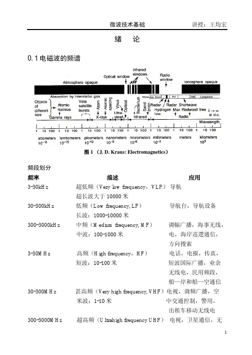
绪论0.1电磁波的频谱图 1 (J. D. Kraus: Electromagnetics)频段划分频率描述应用3-30kHz 超低频(Very low frequency,VLF)导航超长波大于10000米30-300kHz 低频(Low frequency, LF)导航台,导航设备长波:1000-10000米300-3000kHz 中频(Medium frequency, MF)调幅广播,海事无线,中波:100-1000米电,海岸巡逻通信,方向搜索3-30MHz 高频(High frequency,HF)电话,电报,传真,短波:10-100米短波国际广播,业余无线电,民用频段,船—岸和船—空通信30-300MHz 甚高频(Very high frequency, VHF)电视,调频广播,空米波:1-10米中交通控制,警用,出租车移动无线电300-3000MHz 超高频(Ultrahigh frequency UHF)电视,卫星通信,无分米波:1-10分米线电探空仪,监视雷达,导航设备3-30GHz 特高频(Superhigh frequency, SHF)机载雷达,微波传送,厘米波:1-10厘米卫星通信30-300GHz 极高频(Extreme high frequency, EHF)雷达毫米波:1-10毫米300GHz-3000GHz 太赫兹太赫兹技术0.2微波毫米波微波的频率范围不同的书有不同的说法,有将300MHz—30GHz、波长:1cm—1m特指微波;也有称300MHz—300GHz、波长:1mm—1m为微波;还有将300MHz—3000GHz、波长:0.1mm—1m统称为微波。
细分:微波:300MHz—30GHz,波长:1cm—1m毫米波:30GHz—300GHz,波长:1mm—1cm亚毫米波:300GHz—3000GHz,波长:0.1mm—1mm微波频段划分频段标称波长旧波段新波段500-1000MHz VHF C1-2GHz 22cm L D2-3GHz 10cm S E3-4GHz S F4-6GHz 5cm C G6-8GHz C H8-10GHz 3cm X I10-12.4GHz X J12.4-18GHz 2cm Ku J18-20GHz 1.25cm K J20-26.5GHz K K26.5-40GHz 0.8cm Ka K40-60GHz 0.6cm U60-80GHz 0.4cm V80-100GHz 0.3cm W微波毫米波的特点低于1GHz的通信电路通常由集总参数电路元件构成,超过1GHz到100GHz,集总元件被传输线和波导元件取代。


微波光子学的基础理论与实验研究一、微波光子学的概述微波光子学是研究微波与光之间相互转换的一门学科,其基础理论主要涉及光学、电磁场理论、半导体和微波技术等多个学科。
这是一门富有活力的研究领域,特别是在通信、医疗、测量和安全等领域,有着广泛的应用。
同时,微波光子学在量子计算和量子信息处理方面也具有非常重要的应用价值。
二、微波和光的相互作用微波和光之间可以通过电光效应相互转换。
电光效应源于晶体结构中的对称性,可以引起光线的折射或损耗,产生相位差。
在微波和光的相互作用中,把微波和光耦合在一起,然后通过电光、光电和非线性光学效应实现脉冲延迟、解调和调制等操作。
在此过程中,一些光电器件(如光纤、微波毫米波器件、微波光纤和光探测器)被广泛应用,这些器件不仅提供了光电互转接口,同时也增强了微波和光的耦合效率。
三、微波光子学的基础理论微波光子学的基础理论包括电光效应和光电效应两个方面。
电光效应是指光的电场与结构中的电场相互作用,出现折射率的变化;光电效应是指电子在光场中的受激发射和吸收过程。
1、电光效应电光效应主要包括三种:Kerr效应、Pockels效应和 Mach-Zehnder 消光器。
Kerr效应是指当介质中的电场受到光场作用时,折射率也随之改变,这种效应在光纤通信中常用于实现脉冲调制和光源调制。
而 Pockels效应是指当介质中的电场恒定时,光的折射率随之变化,广泛应用于大气光学、光通信、雷达和激光交叉测量等领域。
Mach-Zehnder 消光器则是一种基于电光现象的调制器件,其优点是带宽宽、驱动电压低,被广泛应用于光通信、光纤陀螺仪和高精度光学测量等领域。
2、光电效应光电效应包括弗朗霍夫效应、光伏效应、压电效应和反常霍尔效应。
其中,光伏效应是将光能转化成电能的一种光电效应,在太阳能及电池中得到广泛应用;压电效应是指晶体在外电场作用下的扭曲和变形;反常霍尔效应是指在半导体材料中,在磁场的作用下,出现横向电场,产生反常电导现象。
功率器件仿真基本方法对于微波大功率有源器件来说,其输入输出阻抗是一个关键的参数,且不易测量。
而在设计中,没有这些参数,设计将无从下手。
目前微波大功率的有源器件大多采用金属氧化物半导体场效应晶体管(LDMOSFET-Lateral Diffused metallic oxide semiconductor field effect transistor),因此本文以LDMOS功率管的仿真为例探讨微波有源器件仿真。
由于大家所公认的大功率器件仿真的难度,特别是在器件模型建立方面的难度,使得这一工作较其他电路如小信号电路仿真做的晚,且精度也较小信号电路低。
目前公司内部在这方面所作的工作也相对较少。
随着技术的发展,目前的很多仿真软件已经做的很完善,如ADS,它可以提供各种数字和模拟系统及电路的仿真平台,用户的主要任务就是给目标器件建模和搭建电路。
而目前我们使用的主流LDMOS器件即Motorola的大部分器件均提供ADS仿真的模型,我们只要直接使用,这给我们的仿真工作带来了极大的方便,极大的减小了工作量,并提高了准确度。
本文主要探讨使用ADS2002仿真计算大功率LDMOS器件的工作点、输入输出阻抗及其对应的线性指标、电流、增益等电参数。
1LDMOS器件模型首先我们了解一下Motorola的LDMOS器件库的情况。
图1.1是其在原理图中的符号。
图1.1 Motorola LDMOS器件模型它的器件分为两类:单管(MRF_MET_MODEL & MRF_ROOT_MODEL)和对管(MRF_MET_PP_MODEL & MRF_ROOT_PP_MODEL)。
从上面的名称我们可以看出,每一个管子有两个模型,即MET模型和ROOT模型。
MET LDMOS 模型(Moto Electro Thermal Model)是一个经验大信号模型,它可以精确的描述在任意的偏置点和环境温度下的电流电压特性。
其大信号和小信号模型分别如图1.2和图1.3所示[1]。
微波技术的理论与应用案例分析微波技术是一种近年来快速发展的新兴技术,在物联网、5G 通信、雷达探测等领域具有广泛应用。
本文将对微波技术的理论及其应用案例进行深入分析。
一、微波技术的基本理论微波技术的基本理论包括电磁波理论、微波器件及电路理论、微波传输线理论等。
其中,电磁波理论是微波技术的核心理论,它揭示了电磁波在空间中传播的规律,包括电磁波的波长、频率和速度等。
微波器件及电路理论是微波技术的基础,它主要研究微波器件的设计及其电路的布局,如微波管、微波晶体管、微波集成电路等。
此外,微波传输线理论研究了在微波频段内的电磁场等效电路模型、传输线参数的计算、阻抗匹配等关键技术。
这些基本理论的掌握对于微波技术的应用具有重要意义。
二、微波技术在雷达探测中的应用雷达探测是微波技术的一个典型应用领域,由于微波具有穿透性强、抗干扰能力好等特点,所以在雷达探测中具有广泛的应用。
雷达探测主要包括气象雷达、海洋雷达、地球观测雷达等。
气象雷达主要用于对大气中云和降水的探测,其工作频率通常为S波段(2~4GHz)。
海洋雷达主要用于对海洋水面的探测,其工作频率通常为X波段(8~12GHz)。
而地球观测雷达主要用于对地球表面的探测,如地质勘探、环境监测等,其工作频率通常为Ku波段(12~18GHz)。
三、微波技术在通信中的应用微波技术在通信中的应用也十分广泛。
在移动通信方面,5G通信正式商用,它采用的是28GHz和60GHz等超高频微波信号,具有更高的传输速率和更低的延迟,可以实现更加高效的数据传输,为智能制造、智慧城市等领域的发展提供了新的动力。
在卫星通信方面,微波通信技术也得到广泛应用,如卫星通信、导航系统、卫星地球传感器等。
它具有信号传输距离远、抗干扰性好等特点,能够满足遥感数据传输、卫星导航等需要。
此外,在军事通信等领域也有着重要的应用。
四、微波技术在应急救援中的应用微波技术在应急救援中的应用也十分重要。
在自然灾害和突发事件中,微波技术可以通过无线通信、遥感探测等方式实现快速救援和灾后评估。
Basic BJT CircuitFigure 1 below shows the simplied ‘Pi’ model of a BJT.cVinVoutZinVoutBCΒ.ib ibFigure 1 Transistor symbol and simplified ‘Pi’ modelWe can see that output consists of a current source –gm.Vbe to get the output voltage we multiply by the load resistance Rce ie Vout = -gm.Vbe.Rce (the negative sign denotes signal inversion).The input resistance of the circuit is given by:e temperatur room at (23.5mV)0.0235V ely approximat is and voltage thermal the as known is V (mS)ctance Transcondu gm Kelvin in e Temperatur T 1.6022x10 charge Electron q 1.3807x10 constant Boltzmansk where q k.T V ; V I gm where gmβR T 19-123-T T CQ IN =========−CJKThe output resistance is given by:ge(V)EarlyVolta V Where I Vrce R A CQA OUT ===The voltage gain (Av) is given by:TA CQ A T CQ be be IN OUT V V VI V .V I rce . V rce .V . V V A ==−=−==gm gmThe current gain (Ai) is given by:β- i β.i - I I A bbIN OUT i ===The MOS TransistorThese devices are known as FET’s (Field effect transistors), which consist of three regions source, drain and gate. The resistance path between the drain and source is, controlled by applying a voltage to the gate. This varies the depletion layer under the gate and thusreduces or increases the conductance path. The FET input impedance (unlike the BJT which is a few K Ω) is very high (~M Ω’s) and as a result the gate current can be considered as zero.As per the BJT the FET is best described by it’s Output I-V DC characteristics (N-typeenhancement characteristics shown below), however things are complicated by the fact there are two types of FET depletion and enhancement that are both available as N-type or P-type devices. For low frequencies the enhancement devices is more commonly used (Depletion mode types will be described when discussing microwave devices).0 = 0V123Triode Region Or Linear RegionGST GS DS V V V −=(1) Cut-Off Region – In this region the gate voltage is less than the pinch-off voltage Vp and therefore very little current flows.(2) Triode Region – In this mode the device is operating below pinch-off and is effectively a variable resistor. R OUT is ~ linear but only over a small range of V DS .(3) Saturation Region – This is the main operating region for the device. The drain voltage has to be greater than the gate voltage less the pinch-off voltage – this sets the minimumsupply voltage. The curves in the saturation region can be extrapolated to a point 1/λ, where λ is known as the ‘Channel length modulation parameter, (units V -1), - this is analogous to the BJT Early voltage.Referring to the saturation region we can assume the response is approximately linear such that the:-resistance high e,conductanc small ie λ.I G λ1I λ1V I V 1if then0.01 to 0.001 region the in typically is λλ1V I G therefore 1I .G1- VDS then c mx - y form the of line straight a assume we If G e conductanc output Device curve of slope R resistance output Device curveof slope 1D O DDS D DS DS D O D OOO≈−−=⎟⎠⎞⎜⎝⎛−−>>⎟⎠⎞⎜⎝⎛−−=+⎟⎟⎠⎞⎜⎜⎝⎛=+===λλTo complete the model for the FET we need to add the term for the linear region which, is dependant on the device mobility and gate dimensions.I ()DS DS DS DS DS DSO DQ DQ D λ.V 1.I .V λ.I I .V G I I I +=++∆+=DS DS T GS OX O V .2-V -V .L .C .⎥⎦⎤⎢⎣⎟⎠⎜⎝µ()()parametermodulation length Channel voltagethreshold Device VT ratio aspect the as Known W/L length channel Effective L widthchannel Effective W oxidegate of area unit per e capacitanc tC device of mobility Surface Where onlyregion /linear saturation -non .V 1V .2V -V -V .L W .C . ID OXOX OX O DS DS DS T GS OX O ========+⎥⎦⎤⎢⎣⎡⎟⎠⎞⎜⎝⎛=λεµλµFor saturation region ie V DS > (V GS -V T )[]()[]()parameterctance transcondu Intrinsic the as Known .C µ K Where λ.V 1V -V 2L W .KI aswritten -re Sometimes parameter ctance transcondu the as Known 2L W .C µβ Where λ.V 1V -V β I OX O P DS 2T GS P D OX O DS 2T GS D =+⎦⎤⎢⎣⎡=⎥⎦⎤⎢⎣⎡=+=Usually λ.V DS << 1 so[]2T GS D V -V β I ≈The following page shows some typical values of the above parameters for use with a level 1 MOS model. The ADS version of this model is also shownTypical MOS Spice Parametersn-Well CMOS Level 1 SPICE Model parametersLevel 1 SPICE Parameter n-channelMOSFETp-channelMOSFETUnitsGate oxide thicknessTOX150 150 Angstrom TransconductanceParameter KP50 x 10-625 x 10-6Amp/V2 Threshold Voltage VT0 1.0 -1.0 VoltsChannel-length modulation parameter LAMBDA 0.1/LL in micron0.1/LL in micronV-1Bulk ThresholdParameter GAMMA0.6 0.6 V1/2Surface Potential PHI 0.8 0.8 VGate-drain overlapcapacitance CGDO5 x 10-10 5 x 10⁻¹⁰F/mGate-source overlapcapacitance CGSO5 x 10-10 5 x 10⁻¹⁰F/mZero-bias planar bulkdepeletioncapacitance CJ10-4 3 x 10⁻⁴F/m2Zero-bias sidewall bulkdepletion capacitanceCJSW5 x 10-10 3.5 x 10⁻¹⁰ F/mBulk junction potentialPB0.95 0.95 V Planar bulk junctiongrading coefficient MJ0.5 0.5 None Sidewall bulk junctiongrading coefficientMJSW0.33 0.33 NoneVAR VAR2LAMBDA=0.1/LL=0.5W=100MOSFET_NMOS MOSFET1Mode=nonlinearTemp=Region=Mult=Nrs=Nrd=Ps=Pd=As=Ad=Width=W um Length=L um Model=MOSFETM1LEVEL1_Model MOSFETM1AllParams=Imax=Ffe=Tt=N=Tnom=Rds=Rg=Fc=Af=Kf=Gdsnoi=1Nlev=Uo=Ld=Tpg=Nss=Nsub=Tox=150e-10Js=Mjsw=0.33Cjsw=5e-10Mj=0.5Cj=1e-4Rsh=Cgbo=Cgdo=5e-10Cgso=5e-10Pb=0.95Is=Cbs=Cbd=Rs=Rd=Lambda=LAMBDA Phi=0.8Gamma=0.6Kp=50e-6Vto=1PMOS=no NMOS=yesAs with the BJT it is possible to simulate a device under ADS to produce the device Output I-V curve trace for a typical N-type MOS 3.3V 0.25um process enhancement device. The Spice data for the MOSFET model is called up from the spice file ‘tsmc_’.spiceInclude SPICE1File="tsmc_"NetlistDebugMode=0VAR VAR1VDS=0VGS=0DC1SweepVar="VDS"Start=0Stop=3.3Step=.1Other=OutVar="MOSFET1.Gm"Sweep1SweepVar="VGS"SimInstanceName[1]="DC1"SimInstanceName[2]=SimInstanceName[3]=SimInstanceName[4]=SimInstanceName[5]=SimInstanceName[6]=Start=0Stop=2Step=0.2The resulting plot0.00.51.01.52.0 2.53.0 3.5-55 1015 20 25 30 35 40 45 VgsVDSIDS.i, mAThe device will also have a transconductance Curve ie V GS vs I DS . The ADS simulation below sweeps the gate voltage and measures the resulting drain current.DC1Other=OutVar="MOSFET1.Gm"Step=.1Stop=3Start=0SweepVar="VGS"VAR VAR1VDS=3.3VGS=0spiceInclude SPICE1File="tsmc_"NetlistDebugMode=0Resulting transconductance curve, slope is the G M of the device.0.00.20.40.60.81.0 1.2 1.4 1.6 1.82.0 2.2 2.4 2.62.83.00.0000.0050.0100.0150.0200.0250.0300.0350.0400.0450.0500.0550.0600.0650.0700.0750.0800.085VGSIDS.iSlope of curve = gmIDS (A)Pinch-off voltage = 0.6VAnd for the P-type deviceInput transconductance traceMOSFET_PMOS MOSFET1Mode=nonlinearTemp=Region=Mult=2Nrs=Nrd=Ps=Pd=As=Ad=Width=100 um Length=0.5 um Model=MODpch3_1DC1Other=OutVar="MOSFET1.Gm"Step=-.1Stop=-5Start=0SweepVar="VGS"VAR VAR1VDS=-3.3VGS=0spiceInclude SPICE1File="tsmc_"NetlistDebugMode=0Resulting trace-5-4-3-2-1-0.07-0.06-0.05-0.04-0.03-0.02-0.010.00VGSIDS.ispiceInclude SPICE1File="tsmc_"NetlistDebugMode=0MM9_NMOS MOSFET1Mode=nonlinearMult=2Temp=Lg=Ls=Ab=Width=100 um Length=0.5 um Model=MODnch3_1ParamSweep Sweep1Step=1Stop=5Start=0SimInstanceName[6]=SimInstanceName[5]=SimInstanceName[4]=SimInstanceName[3]=SimInstanceName[2]=SimInstanceName[1]="DC1"SweepVar="VGS"DC1Other=OutVar="MOSFET1.Gm"Step=.1Stop=3Start=0SweepVar="VDS"VAR VAR1VDS=3.3VGS=0Output characteristic trace-5-4-3-2-1-0.07-0.06 -0.05 -0.04 -0.03 -0.02-0.01 0.00 0.01 VDSIDS.iBody EffectThe FET body or ‘Bulk’ is known either as the substrate, back gate or more commonly the Body. It is normally connected to the lowest voltage potential of the circuit (usually thesource). However if is left unconnected its effect on the DC characteristics of the device must be taken into account. If we include the bulk effect the value of the threshold voltage V T will increase with increasing bulk voltage.()source) the to connected bulk (ie 0 V for V V normally Therefore,(Volts)potential source Bulk V (Volts) potential level Fermi .F (Volts)parameter hold Bulk thres γ.F 2..F 2.V -γ V V BS T TO BS BS TO T ====Φ=Φ−Φ++=If the device was biased without the bulk node connected then a change in operating point could take the device out of its saturation region and significantly change the circuitperformance. The bulk voltage is thus a very important parameter in circuit applications and therefore it is best to connect the bulk to the device source connection.The circuit is drawn as follows:-The simulation below shows how varying the bulk voltage will vary the pinch-off voltage of the device.VAR VAR1VBS=0VGS=0Sweep1Step=0.1Stop=1Start=0SimInstanceName[6]=SimInstanceName[5]=SimInstanceName[4]=SimInstanceName[3]=SimInstanceName[2]=SimInstanceName[1]="DC1"SweepVar="VGS"DC1Other=OutVar="MOSFET1.Gm"Step=0.5Stop=3Start=0SweepVar="VBS"V_DC SRC4Vdc=VBSspiceInclude SPICE1File="tsmc_"NetlistDebugMode=0Resulting plot showing that the pinch-off voltage increases with increasing bulk voltage0.00.20.40.60.8 1.00.0000.0010.0020.0030.0040.0050.0060.0070.008IDS.iIncreasing pinch-off voltageFrom the last section we found that the drain current in the saturation region =[]2T GS D V -V β I ≈Transconductance[][][][][]D 5.0D 0.50.5-5.0D 1D DT GS 2T GS D T GS GST GS D GS 2T GS D GSD M I .β2 I .2β βI .2β βI 2βGM (1) into sub βIV -V then V -V β I rearrange we If(1) - V -V 2β GM V .V -V 2β I V wrt ate differenti therefore V -V β I curvetransfer of slope ie V IG =======∆=∆=∆∆=Output Conductance()()()()λ.I G V I V λ..I I (2)into sub V -V βI above From (2) - V λ..V -V β I V wrt ate Differenti λ.V 1V -V βI sticcharacteri output of slope ie ∆V ∆I G D O DSDDS D D 2T GS D DS 2T GS D S D DS 2T GS D DSDO ==∆∆=∆=∆=∆=∆+==Voltage Gain AL .W K .I 2.λ1 .I .L .2.W .K .λ2 I 1.2L .W K .λ2 2L .W K β and I β.λ2 A .λI .2.β .λ.I I .2.β λ.I β.I 2 G G e Conductanc Output ctance transconduA P D 0.5-D 0.5-0.5-0.50.5P 1-1D P P D10.5-D 0.511D 0.5D 0.5DD O M ==========−−−Common-Base/Gate CircuitsCommon-Base BJT circuitThe figure below shows the simplied ‘Pi’ model of a common-base BJT.r ceVinZinV I e wher gm 1r 1)(βi 1).r (βi I V R TCQ be b be b IN IN IN ===++==gm)r gm1(as V V I V .V I r r 1)r (βr .β 1)r (βi r .i .β V V A ce T A CQ A T CQ be ce be ce be b ce b IN OUT V ===≈+=+==()1 1ββ)1βi β.i I I A b b IN OUT i ≈+=+==r ceTo determine the Output impedance of the circuit we can connect a voltage source (V s + R s ) to the base and ground the input ie the emitter. We then have to resistances in parallel connected to the current source β.i b .()equationabove into sub R r R i i Also r .i r i .i V i VR sbe sT b be b ce b T OUT TOUTOUT +=++==βsbe be s s be s ce ce T OUT OUT be s ce sT ce s be s T TOUT R r r.R R r R r .r i V R r .R r R i r R r R i .i V ++++==++⎟⎟⎠⎞⎜⎜⎝⎛++=ββ()ce ce ce OUT s ceOUT s r .1 1r .r R then large R If r R then 0 R If +=++====ββCommon-Gate MOSFET Circuitgr dsVoutVinI INVoltage Gain A v()R r .R r gm A //R r gmVsg V Vsg V V VA L dgL dg V L dg O IN INOV ⎟⎟⎠⎞⎜⎜⎝⎛+====Input ResistanceλI gm1 gmVgs Vgs I VR D IN IN IN ====Output ResistanceAs the source is low impedance ie close to ground for R OUT – r ds appears to be connected across r ds to ground.ds dg OO OUT //r r I VR ==Current Gain A iA i = 1Common-Emitter/Source CircuitsCommon-emitter BJT circuitThe figure below shows the simplied ‘Pi’ model of a common-emitter BJT.VoutEBCΒ.ib ibVinVoutZin(mS)ctance Transcondu Kelvinin e Temperatur T 1.6022x10charge Electron q 1.3807x10 constant Boltzmans k whereq k.T V ; V I where R 19-123-T TCQ IN =========−gm C JK gm gm βge(V)EarlyVolta V Where I Vrce R A CQA OUT ===TA CQ A T CQ be be IN OUT V V VI V .V I rce . V rce .V . V V A ==−=−==gm gmββ- i .i - I I A b bIN OUT i ===Common-Source MOS FET CircuitdrainVoutsd IoVoltage Gain A v()R r .R r gm - A //R r gmV - V V VA L dsL ds L ds IN O INO V ⎟⎟⎠⎞⎜⎜⎝⎛+=== Input ResistanceR IN = ∞Output ResistanceL ds OOOUT //R r I VR ==Current Gain A iA i = ∞Common-Collector/Drain CircuitsCommon-Collector Drain BJT CircuitFigure 1 below shows the simplied ‘Pi’ model of a common-collector BJT.B Cβ.i bi bVinZinLLLLLLggoR1rce1'R1Rrcerce.R'R+=+=+='.R)1('RrII).1('RI.rIVVIVRLLbebbLbbeINRLbeINININβββ≈++=++=+==rceRthenrceRifRrcee.Rr'R1).i('R.1).i(IVROUTLLLLbLbOUTOUTOUT≈<<+==++==cββ1)(bybottom&topdivide)1('Rr)1('RI).1('RI.rI).1('RVVALbeLbLbbebLINOUTV++++=+++==βββββLLLLVbeLbeLVggo'R1abovefrom'R)1(.'RAgmr'R)1('RA+=++=∴=++=ββββgm1)1(.ggo1ggobybottom&topMultiplyggo1)1(.ggoggo1ALLLLLV+++=++++++=ββββgm gmδαδββα.11A gm g go let and 1Let V L +=+=+=()()βββ 1 i i .1I IA b b INOUT i ≈+=+==Common-Drain MOS FET CircuitdrainVoutVindVoltage Gain A v()()()()()()1A 1AAv Therefore, //R r gm Av //R r gm 1//R r gm Av by Vgsbottom & top divide //R r gmVgs Vgs //R r gmVgsAv //R r gmV Vo V V VV VAv L ds L ds L ds L ds L ds L ds gs Ogs OIN o ≈+==+=+==+==Input ResistanceR IN = ∞Output Resistancegm1I V R O O OUT ==Current Gain A iA i = ∞Common-Emitter Circuit with emitter degenerationThe figure below shows the simplied ‘Pi’ model of a common-emitter BJT with emitter de-generation.VinBCβ.ib ibVinVoutZinZoutLce L ce L EL E L E be L E b be b L b IN OUT V R r .R ris 'R Where R 'R - R 'R .- 1)R (βr 'β.R - 1)R (βi .r i 'R ..βi - V V A +=≈≈++=++==αE E be bEb be b IN IN IN 1)R (β 1)R (βr i 1)R (βi .r i I V R +≈++=++==ββ i .i I IA bbIN OUT i ===VoutTo determine the Output impedance of the circuit, we ground the base and the emitter. We then have two resistances in parallel connected to the current source β.i b .()()equation above into sub r //R i V Also V r gmV i Vi VR be E T be bece be T OUT TOUT OUT +=++==()()()()()()()()()()⎟⎟⎟⎟⎠⎞⎜⎜⎜⎜⎝⎛++==⎟⎟⎟⎟⎠⎞⎜⎜⎜⎜⎝⎛++=⎟⎟⎠⎞⎜⎜⎝⎛++=−++==++=++=1βgm.R R .gm 1r R βgm r 1 and 1r R R .gm 1r r by bottom and top divide r R r .R .gm 1r R ignored be can and small is term This r //R r //R r //R gm 1r i V R r //R i r //R gm 1.i r r //R i r r //R i .gm i V EE ce OUT be be E E ce be be E be E ce OUTbe E be E be E ce TOUTOUT be E T be E T ce be E T ce be E T T OUT)gmR (1r R gmR if E ce OUT E +=<<βGenerallyThe de-generated CE circuit provides DC regulation but the load andemitter resistors may have similar values and hence the voltage gain will be low. This however, can be overcome by RF bypassing RE, with a smaller RE, resulting in high voltage gain while maintaining the correct DC bias conditions.The circuits below illustrate the problem and solution.Say we require an amplifier with a voltage gain of 15, a C-E voltage of 5V with an Ic current of 5mA to give us best noise performance. If we equally apportion the voltage we get the following circuit:-V INThe voltage gain of this circuit will be ~ – 700/700 = ~ -1, but we can bypass the emitter resistor as shown below:-V INFor DC the capacitor is open circuit and we have the emitter resistor back to 700 Ω. However at high frequencies the capacitor shorts out the 650Ω so that R E is now effectively 46Ω.The gain is now – (700/46) = -15. (-ve because it is inverting).De-generated MOS FET CircuitThe de-generated MOSFET circuit is an extension of the common-drain circuit except in this case we have a load on the drain as well as the source as shown in Figure 1. The resulting gain will be a ratio of R S/R D and the output resistance will ~ R D. The resistance looking into VX will increase and therefore will make this circuit useful as a current sink especially on the differential amplifier tail device where high R improves the CMMR.dI SVXROUT’Figure 1 Schematic and small signal model of the de-generated MOSFET circuit. Output ResistanceFirstly consider in the increase in the output resistance due to R OUT prime.If we apply a current source on V OUT of value I T current will try to flow to ground via the device current source as source resistor. If we tried to force current to flow we would find the voltage would greatly increase as a result of the high resistance R OUT prime.Therefore, referring to figure 2 we can show this circuit.dAs the gate has been grounded then vg = 0,Therefore, Vgs = Vg - Vs = 0 - R S.I TVgs = Vs = -R S.I TThe current source in the device gives rise to a currentI T = gm.Vgs, so theVoltage Vs = -gm.Vgs.RsThe voltage drop across RS adds current to the output ie.The total current at the output will be I T and the current from the current source connected to Rs.()()()()gm.Rs Rds. R then small is Rs as )gmRs Rds(1Rs I )gmRs Rds(1Rs I I VR Now )gmRs Rds(1Rs I Vget to factorise R I .I Rds.gm.R Rds.I ie out multiply R I .I gm.R I Rds V 1equation in Sub R I Rds.Ids Vs Vds V (1)- gm.Rs.I I Ids OUT TT T T OUT T T S T T S T S T T S T T S T T T T ≈++=++==++=++++=+=+=+=This circuit exhibits negative feedback which gives rise to the increased resistance.Voltage Gain (Av)From the above equations we now easily calculate the voltage gain of the degenerated MOSFET circuit ie())gmRs Rds(1Rs I V V and .RsI Vs Vgs V work previous the from V VAv T T OUT T IN INOUT++======()()S IN OUT SIN OUT S T T T IN OUT T T OUT T IN R Rds V V to reduces this so Rds than is term Rds.gm the R Rds.gmRds 1V V R )gmRs Rds(1Rs give to cancel I .Rs I )gmRs Rds(1Rs I V V therefore)gmRs Rds(1Rs I V V and .RsI Vs Vgs V =<<++=∴++++=++=====Input resistanceThe input resistance of the circuit will be very, very high.The ADS simulation of figure 3 shows a simple common-source circuit. However, there is an ideal bias supply to the drain ie supplies only DC and is an open-circuit to AC/RF. There is also a DC decoupled S-parameter termination connected to Vout and set to a very highimpedance. This allows measurement of the resistance looking into the Vout port, setting the termination value very high ensures it doesn’t interfere with the already high impedance caused by Rd.Note for the first plot if figure 4 the value of RS (R3) was set at 0 ohms.The ADS simulation was modified but the value of RS was increased to 2500ohms (there needed to be a slight alteration to the gate bias to restore the drain current back to 10uA).The second simulation plot is shown in figure 5 and shows how the resistance has increased from 9.5M Ω to 13M Ω. S_Param SP1Stop=10 MHzStart=1 MHz S-PARAMETERSDCACW=10EqnVar V_DC SRC1Vdc=5 VFigure 3 ADS simulation set-up for a simple common-source amplifier. ROUT will effectively be defined by Rd of the FET. The S-parameter DC decoupled terminal and simulation box allow the measurement of R OUT .Sheet5 of 5freq, MHzreal(Z(1,1))Figure 4 Simulation of the circuit shown in figure 3 with the source resistor RS (R3) set to 0 ohms (ie the circuit is configured as common-source). Output resistance is 9.5M ohms.real(Z(1,1))freq, MHzFigure 5 Simulation of the circuit shown in figure 3 with the source resistor RS (R3) set to 2500 ohms (ie the circuit is configured common-source with de-generation). Output resistance has now 13M ohms. NOTE there was a slight alteration to the gate bias to restore the drain current back to 10uA.。