Moss-Burstein effect 莫斯-布尔斯坦效应
- 格式:rtf
- 大小:1.44 MB
- 文档页数:7
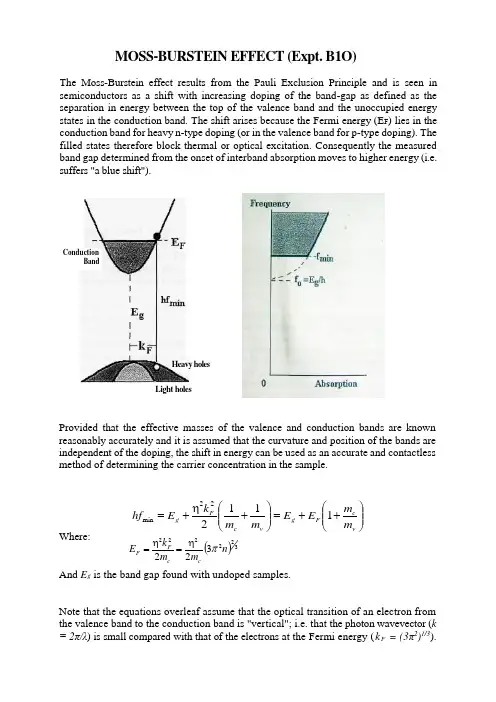
MOSS-BURSTEIN EFFECT (Expt. B1O) The Moss-Burstein effect results from the Pauli Exclusion Principle and is seen in
semiconductors as a shift with increasing doping of the band-gap as defined as the
separation in energy between the top of the valence band and the unoccupied energy
states in the conduction band. The shift arises because the Fermi energy (EF) lies in the
conduction band for heavy n-type doping (or in the valence band for p-type doping). The
filled states therefore block thermal or optical excitation. Consequently the measured
band gap determined from the onset of interband absorption moves to higher energy (i.e.
suffers "a blue shift").
Provided that the effective masses of the valence and conduction bands are known
reasonably accurately and it is assumed that the curvature and position of the bands are
independent of the doping, the shift in energy can be used as an accurate and contactless
method of determining the carrier concentration in the sample.
Where:
And Eg is the band gap found with undoped samples.
Note that the equations overleaf assume that the optical transition of an electron from
the valence band to the conduction band is "vertical"; i.e. that the photon wavevector (k
= 2π/λ) is small compared with that of the electrons at the Fermi energy (kF = (3π2)1/3).
Conduction Band
Heavy holes
Light holes
vcFgvcFgmmEEmmkEhf111
222
min
322222322nmmkE
ccFFCheck that you agree with this assumption taking λ (in air) as 3 microns, the refractive
index of InAs as 3.5 and n = 1024 m-3. By performing the following experiment, and assuming that the conduction and valence
band effective masses are mc = 0.03m0 and mv = 0.4m0 respectively, calculate the carrier
concentration (n) for the doped samples provided (the effective mass at the conduction
band edge is 0.024m0. At the Fermi energy concerned the appropriate effective mass has increased by 50%).
EXPERIMENT
You are provided with a Spex monochromator, a globar source with a germanium
lens, a light chopper, lead selenide and lead sulphide photodetectors and a "Phase
Sensitive Detector" which enhances and amplifies the signal and suppresses noise.
A PC is also available for equipment control and data processing. See Figure 1 for a
schematic of the experimental set-up. Check the zero setting of the monochromator. If the grating were perfectly positioned
it would act as a mirror for all wavelengths at a dial setting of 0000. You will almost
certainly find that the maximum reflection occurs at a slightly different dial reading. Add or subtract this small "zero error" when you calculate the true wavelength. Use
the "mirror" setting to align your source and detector. Provided that you are using
the germanium lens you will not get any diffracted radiation through the
spectrometer until a dial reading of about 3000 is reached and you should obtain a
maximum signal on your detector at a dial reading of about 4000. Remember that the
grating equation is m λ = a sin θ so that you may get second order (m = 2) radiation
through the monochromator at dial settings greater that 6000 (assuming that the Ge
lens cuts in at 3000). Assume that the grating scale is linear in wavelength and that the
wavelength in microns is 6x10
-4 of the dial reading; i.e. that a dial reading of 4000
corresponds to a wavelength of 2.4μm.
Take several 'background' recordings with no sample in place in order to PSD PC
Monochromator Light source and lens
Light chopper
Sample Detector
Figure 1 - Diagram to show the experimental set-up familiarise yourself with the equipment and in order that background features due
to atmospheric absorption may be at least partially removed by ratioing the
transmission with the sample in place with the “background” values.
The 'background' spectrum is limited by the band gap absorption of the Ge lens at
short wavelengths and by the cut-off for intrinsic excitation of the photodetectors
at long wavelengths. Estimate the band gaps of Ge, PbS and PbSe from the
respective background spectra.
Observe the effect of changing the slit-widths on the monochromator on the
atmospheric features at wavelengths at 4.2μm and 2.7μm.
You are given four epitaxial films of InAs of thickness of a few microns grown on
GaAs substrates. One sample is undoped and the others have been fairly heavily doped
with silicon donors. Taking great care, place each metal sample mount in turn over the detector iris in order to take a transmission spectrum. On no account touch the surface of the semiconductor samples as they are very fragile.
The GaAs substrates do not absorb significantly in the wavelength range concerned.
However both the InAs epitaxial film and the GaAs substrate have high refractive
indices and reflect quite strongly. You should be able to observe Fabry-Perot interference fringes from the epitaxial film at wavelengths which are too long for the