SMC6480硬件使用手册1.0
- 格式:pdf
- 大小:923.03 KB
- 文档页数:24
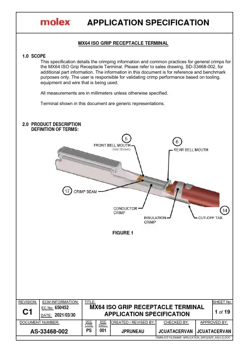
2.0 PRODUCT DESCRIPTIONDEFINITION OF TERMS:REVISION: ECM INFORMATION: TITLE: MX64 ISO GRIP RECEPTACLE TERMINALAPPLICATION SPECIFICATIONSHEET No.C1EC No: 650452 3 of 19DATE: 2021/03/30EXCESSIVE CONDUCTOR BRUSH CONDUCTOR CRIMPThis is the metallurgical compression of a terminal around the wire's conductor. This connection creates a common electrical path with low resistance and high current carrying capabilities.END OF INSULATIONThis is the location where the wire insulation is in relation to the terminal transition area between theconductor and insulation crimps. The conductor strands and insulation jacket must be displaced evenly and visible in the transition area. This position ensures that the insulation is not crimped within the conductor grip. This position can be controlled by the wire stop and/or the wire strip length in bench applications. For automatic wire processing the insulation position is set by the in/out press on the applicator. See Figure 3.BELLMOUTH (FLARE) The flare that is formed on the edge of the conductor crimp acts as a funnel for the wire strands. This flare reduces the possibility that a sharp edge on the conductor crimp will cut or nick the wire strands. For the MX64 ISO Grip terminal a rear bell mouth is required on the conductor crimp while a front bell mouth isoptional. Caution: Excessively large bell mouths will reduce the crimp area which therefore reduces conductor pull forces. See Table 3 for bell mouth specifications.Bell mouth too largeReduced Crimp Area, Lower Pull Forces Bell Mouth per specificationFIGURE 6 – BAD CRIMP FIGURE 7 – GOOD CRIMPCONDUCTOR BRUSH The conductor brush is made up of the wire strands that extend past the conductor crimp into the transition area towards the terminal box. This helps ensure the mechanical compressions occur over the full length of the conductor crimp. The conductor brush should not extend past the transition area into the terminal box.FIGURE 8 - BAD CRIMPFIGURE 9 - GOOD CRIMPFor the MX64 ISO Grip Receptacle Terminal, the conductor brush must be visible past the conductor crimp but must not exceed 0.55mm and, depending on where the brush ends, it must be below the conductor crimp height or below the transition wall (whichever is taller). See Figure 10 for an example of brush height boundary. [Caution: Excessive brush that extends above the crimp height/transition wall can cause terminal retention issues inside the plastic cavity and can potentially tear mat seals]. See Figure 3.5 CONDUCTOR BRUSH FLUSH OR BELOW CRIMP674REVISION:ECM INFORMATION: TITLE:MX64 ISO GRIP RECEPTACLE TERMINALAPPLICATION SPECIFICATIONSHEET No.C1EC No: 650452 4 of 19DATE: 2021/03/30FIGURE 10STRIPPING LENGTH The stripping length is determined by measuring the exposed conductor strands after the insulation isremoved. The stripping length in conjunction with the end-of-insulation position will affect how much the brush length extends past the conductor crimp.CONDUCTOR CRIMP HEIGHT The conductor crimp height is measured from the top surface of the formed crimp to the bottom most radial surface. Do not include the extrusion points in this measurement. Measuring the crimp height is a quick, non-destructive way to help ensure the metallurgical compression of the terminal around the wire's conductor is correct and it is an excellent attribute for process control. The crimp heights specified in this document are set specifically for an explicit type of wire to promote its electrical and mechanical performances. See Table 2 for crimp height specifications.INSULATION CRIMP HEIGHT Insulation crimp heights are specified in Section 3.0, Table 2. The MX64 ISO Grip Receptacle terminals are designed to accommodate multiple wire sizes. Even though the insulation grip may completely surround a smaller wire and only partially surround a larger wire, an acceptable insulation crimp is still provided.The insulation crimp should be visually evaluated to confirm it provides an adequate compression on the wire. It should also be evaluated by sectioning through the center of the crimped insulation grip. The grip should compress the wire but not pierce it or otherwise damage the integrity of the insulation. The grip should not contact the conductors under any circumstance.Once the optimum setting for the application is determined it is important for the operator to check and document the insulation crimp height.1189REVISION:ECM INFORMATION: TITLE:MX64 ISO GRIP RECEPTACLE TERMINALAPPLICATION SPECIFICATIONSHEET No.C1EC No: 650452 5 of 19DATE: 2021/03/30EXTRUSIONS (ANVIL FLASH) These are the burrs that form on the bottom of the conductor crimp resulting from the clearance betweenthe punch and anvil tooling in the crimp applicator. Excessive extrusion will also occur when the anvil is worn or the terminal is over-crimped. An uneven extrusion may also result if the punch and anvil are misaligned, if the feed is misadjusted or if there is insufficient and excessive terminal drag. The crosssection should be examined for any resulting cracks in the material. Cracks can undermine the integrity of the crimp and are not allowed under any circumstance. Caution: Anvil flash has the potential to cut mat-seals and should be maintained with specifications. See Section 3.0, Table 3 for anvil flash specifications.FIGURE 11CUT-OFF TAB LENGTH This is the material that protrudes outside the insulation crimp after the terminal is separated from the carrierstrip. A cut-off tab that is too long may expose a terminal outside the housing and it may fail the electrical spacing requirements. See Section 3.0, Table 3 for cut-off tab length specifications. Caution: Burrs on the cut-off tab are not allowed as they have the potential to cut mat-seals.FIGURE 120.1 mm max.LOWEST POSITION1341349 149REVISION:ECM INFORMATION: TITLE:MX64 ISO GRIP RECEPTACLE TERMINALAPPLICATION SPECIFICATIONSHEET No.C1EC No: 650452 6 of 19DATE: 2021/03/30CRIMP BULGE Caution needs to be taken with the crimp tooling to prevent any bulging between the terminal box and theconductor crimp exceeding the box width at the maximum material condition (MMC). The transition from the conductor grip to the box should flow smoothly with no bulging. If any bulging shall occur between the conductor grip and the terminal box it must not exceed the MMC width of 1.95mm.Any bulging between the conductor crimp and insulation must not exceed the insulations maximum allowable width of 2.05mm. See Figures 13 and 14 below.GRIP STEPThis is the designed offset between the terminal box and the conductor or insulation grip. The grip step should not be altered during the crimping operation. See section 3.0, Table 3 for grip step specifications.FIGURE 15FIGURE 13 - NO BULGEFIGURE 14 - WITH BULGE1.95mm MAX. 189 2.05mm MAX.sample length of 22mm as shown in Figure 16.REVISION:ECM INFORMATION: TITLE:MX64 ISO GRIP RECEPTACLE TERMINALAPPLICATION SPECIFICATIONSHEET No.C1EC No: 650452 8 of 19DATE: 2021/03/30TABLE 2TERMINAL ORDER No.VALIDATED WIRECONDUCTORCRIMP INSULATION CRIMP PULL FORCE MINIMUM(N)LEFT PAYOFF “D” WIND RIGHT PAYOFF “B” WIND CCH (mm) CCW (mm)± 0.05ICH † (mm) ± 0.10 ICW † (mm) ±0.10 SIZE TYPENo. OFSTRANDSINSULATIONMAX OD(mm)33467-0021 33468-0021 34736-0025 33467-0022 33468-0022 34736-0026 0.35mm 2 FLR2X-A 1, a 7 1.30 0.96±0.031.401.551.745033467-0021 33468-0021 34736-0025 33467-0022 33468-0022 34736-0026 22 AWG TXL 1, b 7 1.651.02±0.041.851.8033467-0023 33468-0023 34736-0027 33467-0024 33468-0024 34736-0028 0.50mm 2T3ZHID 1, c 19 1.60 0.99±0.04 1.801.90 1.8975FLR2X-A 1, a19 33467-0023 33468-0023 34736-0027 33467-0024 33468-0024 34736-0028 20AWGTXL 1, b7 1.85 1.00±0.051.951.9533467-0023 33468-0023 34736-0027 33467-0024 33468-0024 34736-0028 0.75 mm 2 FLR2X-A 1, a 19 1.80 1.08±0.05 2.10 1.939033467-0023 33468-0023 34736-002733467-0024 33468-0024 34736-002818AWGTXL 1, b192.061.15±0.052.101.95The above specifications are guidelines for an optimum crimp. Crimp heights/widths are applicable for punch/anvil tooling shown in Figures 19 – 22.Pull force should be measured with no influence from the insulation crimp.Customers are required to complete their own validation testing if tooling and/or wire is different than what is shown in this specification.†Values indicated below are the maximum size permitted for MX64 ISO terminals crimped to wires other than those shown in Table 2 above:Small Grip (Grip Code A) terminals: ICH Max = 2.10mm, ICW Max = 2.05mm Large Grip (Grip Code B) terminals: ICH Max = 2.20mm, ICW Max= 2.05mmTerminal crimps were validated to following specifications:1USCAR-21Wires are in accordance with following specifications:a ISO 6722, GMW15626 (FLR2X-A/T125) and Ford ES-AU5T-1A348-AA (3TAD)b ESB-MIL 123-A & SAEJ1128-TXL typec PSA B25 1110: NTS – Conventional Electrical Conductor910 1112Not required. If present, height from datum [-J-] must not exceed 1.60mm.Seam shall not be open and no wire is allowed outof the crimping areaIn transition from terminal1.95 MAXbox to conductor gripIn transition from conductor2.05 MAXto insulation gripCrimped lead must be able to pass freely through checking aidShown in Section 8.0, Figure 24FIGURE 17 FIGURE 18TITLE:MX64 ISO GRIP RECEPTACLE TERMINAL APPLICATION SPECIFICATIONFIGURE 19TABLE 4U V W X Y Z 33467-002133468-002133467-002233468-002234736-002534736-00267.43 1.75 ± 0.01 4.02 R 5.08 6.07 0.876 ± 0.0133467-002333468-002333467-0024 33468-0024 34736-0027 8.33 1.88 ± 0.01 4.35 R 5.00 6.06 0.94 ± 0.01GENERAL TOLERANCEUNLESS OTHERWISE SPECIFIED 3 PLACES ± 0.012 PLACES ± 0.131 PLACE ±0.25ANGULAR ± ½°GENERAL TOLERANCEUNLESS OTHERWISE SPECIFIED3 PLACES ± 0.012 PLACES ± 0.131 PLACE ±0.25ANGULAR ± ½°FIGURE 20TABLE 5PART No. A B C D E F G H J BB 33467-0021 CHAMFERUNLESS OTHERWISE SPECIFIED2 PLACES ± 0.131 PLACE ±0.25ANGULAR ± ½°FIGURE 21TABLE 6PART No. K L M NGENERAL TOLERANCEUNLESS OTHERWISE SPECIFIED3 PLACES ± 0.012 PLACES ± 0.131 PLACE ±0.25ANGULAR ± ½°FIGURE 22FIGURE 24TABLE 8PART No. DD33467-0021 33468-0021 33467-0022 0.2 ± 0.04GENERAL TOLERANCEUNLESS OTHERWISE SPECIFIED3 PLACES ± 0.01 2 PLACES ± 0.13 1 PLACE ±0.25 ANGULAR ± ½°FIGURE 25 Checking Aid Notes: (Unless otherwise specified)1) Material: Steel 4140 Pre-hardened2) Finish:a) Surface: Block Oxideb) Inside Profile: Polish3) All Dimensions are in inches4) Tolerances are in inches2 Places ± 0.013 Places ± 0.005SUPPLIER CHECKING AID TOOLING PARTNUMBERDESCRIPTION 63867-3008MX64 CRIMPED LEADSTRAIGHTNESS CHECKING。
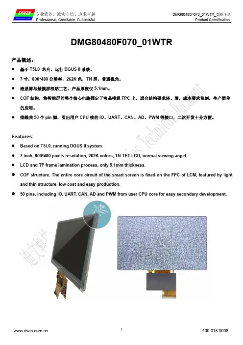
DMG80480F070_01WTR产品概述:●基于T5L0芯片,运行DGUS II系统。
●7寸,800*480分辨率,262K色,TN屏,普通视角。
●液晶屏与触摸屏框贴工艺,产品厚度仅5.1mm。
●COF结构,将智能屏的整个核心电路固定于液晶模组FPC上,适合结构要求轻、薄,成本要求苛刻,生产简单的应用。
●排线共50个pin脚,引出用户CPU核的IO、UART、CAN、AD、PWM等接口,二次开发十分方便。
Features:●Based on T5L0,running DGUS II system.●7inch,800*480pixels resolution,262K colors,TN-TFT-LCD,normal viewing angel.●LCD and TP frame lamination process,only5.1mm thickness.●COF structure.The entire core circuit of the smart screen is fixed on the FPC of LCM,featured by lightand thin structure,low cost and easy production.●50pins,including IO,UART,CAN,AD and PWM from user CPU core for easy secondary development.1外部接口External InterfacePIN 序号Definition 定义I/O Functional Description 功能描述1+5V I 供电输入,DC3.6-5.5V 。
Power supply,DC3.6-5.5V.2+5V I 3GND GND GND4GND GND 5GND GND 6AD7I 5路ADC 输入,3.3V 电源做为参考,12bit 分辨率,输入电压范围0-3.3V 。
SinoMCU 8位集成控制芯片MC30E6080用户手册V1.1本产品为广东晟矽微电子有限公司研制并销售,公司保留对产品在可靠性、功能和设计方面的改进作进一步目录1产品概要 (3)1.1产品特性 (3)1.2订购信息 (4)1.3引脚排列 (4)1.4端口说明 (5)2合封EEPROM (6)3封装尺寸 (7)3.1SOP14 (7)3.2SOP8 (7)4修订记录 (8)1产品概要1.1产品特性⏹8位CPU内核✧精简指令集,5级深度硬件堆栈✧CPU为单时钟,仅在系统主时钟下运行✧系统主时钟下F CPU可配置为2/4分频⏹程序存储器✧1K×14位OTP型程序存储器(烧录1次)✧0.5K×14位OTP型程序存储器(烧录2次)⏹数据存储器✧49字节SRAM/REG型通用数据存储器,支持直接寻址、间接寻址等多种寻址方式⏹2组共12个I/O✧P0(P00~P03),P1(P10~P17)✧P13可配置为单输入口或输入/开漏输出口,可复用为外部复位RST输入,编程时为高压VPP输入✧P15/P14可复用为外部时钟振荡器输入/输出✧P0可配置为内置上拉或下拉电阻,P10~P17内置上拉电阻,P10~P12内置下拉电阻,均可单独使能✧P10~P12/P14~P17可选开漏或推挽输出✧P0可配置为单输出口或输入/推挽输出口,为输入/输出口时可配置使能键盘中断唤醒功能✧P1所有端口均支持键盘中断唤醒功能,并可单独使能⏹系统时钟源✧内置高频RC振荡器(16MHz/8MHz/4MHz/2MHz/1MHz/455KHz),可用作系统主时钟源✧内置低频RC振荡器(32KHz),可用作系统主时钟源✧支持外接高频晶体振荡器(455KHz/1MHz~16MHz),可用作系统主时钟源✧支持外接RC振荡器(0~4MHz),可用作系统主时钟源✧支持外接低频晶体振荡器(32768Hz),可用作系统主时钟源、或定时器RTC时钟源⏹系统工作模式✧运行模式:CPU在系统主时钟下运行✧休眠模式:CPU停止运行,系统主时钟源停止工作⏹内部自振式看门狗计数器(WDT)✧与定时器T0共用预分频器✧溢出时间可配置:4.5ms/18ms/72ms/288ms(无预分频)✧工作模式可配置:开启WDT、关闭WDT,也可软件控制开启或关闭⏹2个定时器✧8位定时器T0,支持外部RTC时钟,可实现外部计数功能,与WDT共用预分频器✧8位定时器T1,可实现外部计数、BUZ、3路共周期独立占空比的PWM(可组合成1对带死区的互补PWM)⏹中断✧外部中断(INT),键盘中断(P00~P07,P10~P17),定时器中断(T0~T1)⏹ 低电压复位LVR✧ 1.8V/2.0V/2.2V/2.4V/2.5V/2.6V/2.7V/2.8V/3.0V/3.2V/3.6V/3.8V ⏹ 低电压检测LVD✧ 1.8V/2.0V/2.1V/2.2V/2.4V/2.5V/2.6V/2.7V/2.8V/3.0V/3.2V/3.3V/3.6V/4.0V/4.2V ✧ 可选择LVDI 输入电压与内部1.08V 比较⏹ 内部合封EEPROM 器件(24C02,器件地址编码为000H ) ⏹ 工作电压✧ V LVR30 ~ 5.5V @ Fcpu = 0~8MHz ✧ V LVR27 ~ 5.5V @ Fcpu = 0~4MHz ✧ V LVR20 ~ 5.5V @ Fcpu = 0~2MHz ✧ V LVR18 ~ 5.5V @ Fcpu = 0~32KHz/2 ⏹ 封装形式✧ SOP14/SOP81.2 订购信息产品名称 封装形式 备注 MC30E6080A0J SOP14 MC30E6080A0HSOP81.3 引脚排列MC30E6080A0JEE_VDD/VDD P00EE_SDA/P17EE_SCL/P16[SDO]/OSCO/P14[VPP]/RST/LVDI/P13GND/EE_GNDP02P03P01P10/INT/TC1/PWM2/[SDO]P11/PWM1/[SDI]P12/TC0/BUZ/PWM0/[SCK]MC30E6080A0JSOP141234567814131211109ERCI/OSCI/P15MC30E6080A0HMC30E6080A0HSOP812348765EE_VDD/VDD [SDO]/OSCO/P14[VPP]/RST/LVDI/P13GND/EE_GNDP10/INT/TC1/PWM2/[SDO]P11/PWM1/[SDI]P12/TC0/BUZ/PWM0/[SCK]P17:EE_SDA P00:EE_SCLERCI/OSCI/P151.4 端口说明端口名称(MCU )类型 功能说明VDD P 电源 GND P 地P00~P03 D GPIO (可配置为单输出口或输入/推挽输出口) 可配置为内部上拉或内部下拉P10~P12 D GPIO (可选推挽/开漏输出),内部上/下拉 P14~P17 D GPIO (可选推挽/开漏输出),内部上拉 P13 D GPIO (可配置为单输入口或输入/开漏输出口) 内部上拉 INT DI 外部中断输入TC0~TC1 DI 定时器T0~T1的外部计数输入 PWM0~PWM2DO 定时器T1的3路PWM 输出 BUZ DO 定时器T1的BUZ 输出 LVDI AI LVD 外部电压输入 OSCI ,OSCOA 外部时钟振荡器输入/输出 ERCI AI 外部RC 振荡器输入 RST DI 外部复位输入SCK ,SDI ,SDOD 编程时钟/数据输入/数据输出接口 VPPP 编程高压输入端口名称(EEPROM )类型 功能说明 EE_VDD P EEPROM 电源 EE_GND P EEPROM 地 EE_SCL DI EEPROM 时钟接口 EE_SDADEEPROM 数据接口 注:P-电源;D-数字输入输出,DI-数字输入,DO-数字输出;A-模拟输入输出,AI-模拟输入,AO-模拟输出。
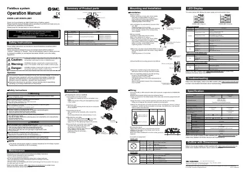
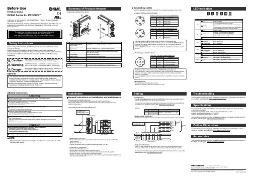
<EX260-SEC1/-SEC2/-SEC3/-SEC4>InstallationConfigurationAuto-increment addressing can be used to address each slave device via its physical position in the communication ring, and not require local address setting.To configure the EX260 SI unit with the EtherCAT master, XML Device Description File is required.The technical document states detail configuration information and the XML file can be found on the SMC website (.)Output number assignmentOutput number starts at zero and refers to the solenoid position on the manifold.General instructions on installation and maintenanceConnect valve manifold to the SI unit.Connectable valve manifolds are same as for EX250 series SI unit.Refer to the EX250 series valve manifold section in the valve catalogue for valvemanifold dimension.Power supply connector layoutGround terminalConnect the ground terminal to the ground.Resistance to ground should be 100 ohms or less.SettingReplacement of the SI unit•Remove the M3 hexagon screw from the SI unit and release the SI unit from the valve manifold.•Replace the SI unit.•Tighten the screws with the specified tightening torque. (0.6 Nm)Precautions for maintenance •Be sure to switch off the power.•Check there is no foreign matter inside the SI unit.•Check there is no damage and no foreign matter being stuck to the gasket.•Be sure to tighten the screw with the specified torque.If the SI unit is not assembled properly, inside PCBs may be damaged or liquid and/or dust may enter into the unit.Connecting cablesSelect the appropriate cables to fit with the connectors mounted on the SI unit.Fieldbus interface connector layoutTroubleshootingThe technical document states detail troubleshooting information can be found on the SMC website (URL )SpecificationsConnected load: 24VDC Solenoid valve with light and surge voltage suppressor of 1.5 W or less (manufactured by SMC)Current consumption of power supply for SI unit operation: 0.1 A max.Ambient temperature for operation: -10 to 50 ℃Ambient temperature for storage: -20 to 60 ℃Pollution degree 2: (UL508)The technical document states detail specification information can be found on the SMC website (URL )Akihabara UDX 15F, 4-14-1, Sotokanda, Chiyoda-ku, Tokyo 101-0021, JAPAN Phone: +81 3-5207-8249 Fax: +81 3-5298-5362URL Outline DimensionsThe technical document states detail outline dimensions information can be foundon the SMC website (URL )AccessoriesThe technical document states detail accessories information can be found on the SMC website (URL )*2: Single flash pattern*1: Blinking patternAssembly and disassembly of the SI unit*3: Flickering patternNOTEWhen conformity to UL is necessary the SI unit must be used with a UL 1310Class2 power supply.Fieldbus deviceOperation ManualEX260 Series for EtherCATThank you for purchasing an SMC EX260 Series Fieldbus device (Hereinafter referred to as "SI unit" ).Please read this manual carefully before operating the product and make sure you understand its capabilities and limitations.Please keep this manual handy for future reference.To obtain more detailed information about operating this product,please refer to the SMC website (URL ) or contact SMC directly.These safety instructions are intended to prevent hazardous situations and/or equipment damage.These instructions indicate the level of potential hazard with the labels of"Caution", " Warning" or "Danger". They are all important notes for safety and must be followed in addition to International standards (ISO/IEC), Japan Industrial Standards (JIS) and other safety regulations.OperatorNote: Specifications are subject to change without prior notice and any obligation on the part of the manufacturer.EtherCAT ®is registered trademark and patented technology, licensed by Beckhoff Automation GmbH, Germany.© 2010 SMC Corporation All Rights ReservedPWR: M12 5-pole Plug A-coded。

三核主板方案领导TMS320C6748开发板使用手册Revision History目录1开发板准备 (4)1.1测试开发板硬件 (4)1.2查看仿真器驱动是否正常安装 (4)2程序烧写 (5)2.1设置工程配置文件信息 (5)2.2测试仿真器是否正常连接 (9)2.3加载GEL文件 (10)2.4CCS连接开发板CPU (11)2.5运行GEL文件来初始化开发板 (12)2.6加载和运行烧写程序C6478_NandWrite.out (13)2.7擦除和烧写Nand Flash (14)2.8镜像格式转换方法 (14)3CCS工程新建和编译 (16)3.1新建工程 (18)3.2编写程序 (21)3.3编译和运行DSP程序 (22)4CCS工程导入和编译步骤 (24)5Demo例程演示 (29)5.1LED (29)5.2KEY (29)5.3UART (29)5.4FFT (30)6附录 (35)6.1Boot Mode Selection (35)前言在进行以下操作之前,请先安装CCS,推荐使用我司验证过的CCS5.5.0版本。
安装包CCS5.5.0.00077_win32.zip可以在TMS320C6748产品资料光盘的tools目录下找到,也可以在TI官网下载,可以下载各种版本的CCS。
下载前需要注册一个TI账号,注册后才能用账号去下载CCS和其他文件,然后再去网上找一个破解文件,安装后按照破解文件指定步骤操作即可正常使用CCS5了。
TI官网下载链接:1 开发板准备1.1测试开发板硬件将开发板的拨码开关1~5号对应拨到00101(说明见附录,1代表ON,0代表OFF,X代表任意,即可以是0也可以是1),这是UART2档位。
RS232串口线通过USB转串口接到PC机的USB口,DB9母头(带孔)接底板UART2口,设置PC机调试终端COM口,波特率为115200,8N1,无检验位。
推荐使用ZOC串口调试终端软件,TMS320C6748产品资料光盘的tools目录下有ZOC的安装包zoc602.zip。
Installation•Direct mounting(1)When joining six or more units, fix the middle part of the complete EX600 unit with anintermediate reinforcing brace (EX600-ZMB1)before mounting using 2-M4x5 screws.Tightening torque: 0.7 to 0.8 Nm.(2)Fix and tighten the end plates at one end of the unit. (M4)Tightening torque: 0.7 to 0.8 Nm.to the operation manual of the corresponding valve manifold.Fieldbus systemOperation ManualEX600-LAB1/EX600-LBB1Thank you for purchasing an SMC EX600 Series Fieldbus system.Please read this manual carefully before operating the product and make sure you understand its capabilities and limitations.Please keep this manual handy for future reference.Safety InstructionsAssemblyComposing the unit as a manifold (1)Connect the unit to the end plate.The Digital unit, Analog unit can be connected in any order.Tighten the bracket of the joint using tightening torque 1.5 to 1.6 Nm.(2)Add more units.Up to 10 units (including the SI unit) can be connected to one manifold.(3)Connecting the SI unit.After connecting the necessary units, connect the SI unit.Connecting method is the same as above (1), (2).(4)Mounting the valve plate.Apply 0.6 to 0.7 Nm tightening torque to the screws.Insert the valve plate to the valve plate set groove on the side of SI unit.Then, tighten it with the valve plate set screws (M4x6) to fix the plate.Tightening torque for set screws0.7 to 0.8 Nm.(EX600-ZMV )•DIN rail mounting(Available for series other than SY series.Refer to the catalog for SY series.)part of the complete EX600 unit with anbefore mounting, using 2-M4x6 screws.Tightening torque: 0.7 to 0.8 Nm.screws.Tightening torque: 0.7 to 0.8 Nm.(5)Fix the manifold by tightening the DIN rail fixing screws of the EX600-ZMA2. (M4x20)Tightening torque: 0.7 to 0.8 Nm.The tightening torque at the valve side depends on the valve type.valve manifold.Wiring•Connect the M12 or M8 connector cable. M12 connector is applicable for SPEEDCON connector.SPEEDCON connector wiring method is explained below.(1)Align the mark B on the metal bracket of the cable side connector (plug/socket) with the mark A.(2)Align the mark C on the unit and insert the connector into the unit vertically.If they are not aligned, the connector cannot be joined properly.(3)When the mark B of the connector has been turned 180 degrees (1/2 turn), wiring is completed. Confirm that the connection is not loose. If turned too far, it will become •Mounting the markerSignal name of the input or output devices and unit address can be written to the marker, and it can be installed to each unit.Mount the marker (EX600-ZT1) into the marker groove as required.OperatorNOTEThe direct current power supply to combine should be UL1310 Class 2 power supply when conformity to UL is necessary.Safety InstructionsMaintenance•Maintenance should be performed according to the Safety Instructions.•Perform regular maintenance and inspections.There is a risk of unexpected malfunction.•Do not use solvents such as benzene, thinner etc. to clean each unit.They could damage the surface of the body and erase the markings on the body.Use a soft cloth to remove stains.For heavy stains, use a cloth soaked with diluted neutral detergent and fully squeezed, then wipe up the stains again with a dry cloth.Refer to the SMC website (URL https://) to obtain more detailed information about maintenance.The status display LED displays the power supply and communication status.TroubleshootingRefer to the LED Display. Refer to the SMC website (URL https:// )to obtain more detailed information about troubleshooting.SpecificationRefer to the product catalog or SMC website (URL https:// ) to obtain more detailed information about product specifications.Outline with DimensionsRefer to the product catalog or SMC website (URL https://) to obtain more detailed information about outline dimensions.Note: Specifications are subject to change without prior notice and any obligation on the part of the manufacturer.© 2019 SMC Corporation All Rights Reserved Akihabara UDX 15F, 4-14-1, Sotokanda, Chiyoda-ku, Tokyo 101-0021, JAPAN Phone: +81 3-5207-8249 Fax: +81 3-5298-5362URL https://Refer to the SMC website (URL https://) to obtain more detailed information about LED display.(3)Hook the DIN rail mounting groove to the DIN rail.(4)Press the manifold using its side hooked to the DIN rail as a fulcrum until the manifold is locked.These safety instructions are intended to prevent hazardous situations and/or equipment damage.These instructions indicate the level of potential hazard with the labels of"Caution", "Warning" or "Danger". They are all important notes for safety and must be followed in addition to International standards (ISO/IEC) and other safety regulations.•Connector pin assignment EX ※※-OMX0005EX600-LAB1 (Class A)EX600-LBB1 (Class B)。
TIDM648EVM板安装平台v1.0TI DM648 EVM板安装平台– windows XP安装步骤(全部安装程序应⽤默认路径)依次按⽂件夹1⾄5次序安装(中途提⽰缺少软件等问题⼀概忽略)1.安装CCS 3.3然后升级CCS3.3⾄3.3 SR822.安装Lyrtech_EVMDM648_Software_Tools3.安装SOC_Analyzer (需虚拟光驱或解压后安装)4.安装DM648_DVSDK_setupwin32 然后安装dvsdk-avinstaller安装完成后右键单击桌⾯“我的电脑”选“属性”> 环境变量> 系统环境变量查看是否以添加BIOSDVSDK_INSTALL_DIR=BIOSUTILS_INSTALL_DIR=\biosutils_1_xx_xxNDK_INSTALL_DIR=\ndk_1_92_xx_xx_eval5.安装dsp_bios_setupwin32安装TDS560USB-Plus仿真器(确认USB接⼊主办USB接⼝以保证电压充⾜,曾遇到接前置板USB端⼝供电不⾜导致⽆法启动仿真器问题)1.确认CSS已升级⾄3.3SR822.运⾏tds560usb_plus_ccs33_SR12.exe3.重启电脑,如提⽰新装硬件需驱动选择drivers⽂件夹下tds560usb_plus.sys⽂件运⾏CSStudio Component Manager 更改DSP/BIOS下的TMS32067xx,选择最新版本运⾏Setup CSStudio v3.31.选择create board 然后选定wintechdigital TDS560plus处新增板卡)3.右侧选取ICEPICK_Ca)Number of router 填写1(如DM6467等带ARM板卡填写2)b)Subpath Name处填写DSPC64 port number填写0x10 (如有arm 则把ARM填写⾄第⼀位dsp更改到第⼆位同时第⼆位port number改为0x12)c)Finish4.DSPC64下选取C6400PLUS 其GEL⽂件地址输⼊DM648GEL⽂件地址例:C:\Lyrtech\EVMDM648\gel\EVMDM648.gel5.完成,关闭CCSetup Studio 选取SA VE 在start code composer studio提⽰上选Y286CLK_F_gethtime = _CLK_gethtime[Linking...] "C:\CCStudio_v3.3\C6000\cgtools\bin\cl6x" -@"Debug.lkf">> warning: creating output section $build.attributes without SECTIONSspecification>>C:/dvsdk_1_11_00_00_DM648/dm648_demo_0_92_04/xdcconfig/package/cfg/dm648_demo_x6 4Pcfg.cmd, line 286: warning:symbol CLK_F_gethtime from fileC:/CCStudio_v3.3/bios_5_33_06/packages/ti/bios/lib/biosDM420.a64P being redefinedBuild Complete,0 Errors, 2 Warnings, 0 Remarks.。
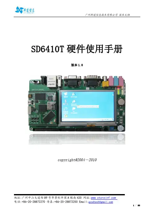
SD6410T硬件使用手册版本1.0copyright@2004-2010版权声明本手册版权归属广州斯道信息技术有限公司所有,并保留一切权力。
未经广州斯道信息技术有限公司许可(书面形式)任何单位和个人不得摘录本手册部分或全部内容。
违者将追究其法律责任!广州斯道信息技术有限公司日期:2010-10-27修订历史:版本号说明作者日期1.0正式发布版Kevin2010-10-27·硬件篇第一章SD6410T开发板介绍41.1SD6410T开发板简介41.1.1SD6410T开发板外观51.1.2SD6410T开发板硬件资源说明61.1.3机械尺寸图81.2S3C6410内部功能框图:101.3Linux系统资源特性111.4WinCE 6.0系统资源特性121.5Android系统资源特性121.6Ubuntu系统特性12第二章SD6410T开发板硬件说明132.1跳线说明132.2接口布局142.3接口定义及资源说明142.3.1系统内存分配图142.3.2电源接口和插座152.3.3串口152.3.4USB接口162.3.5网络接口182.3.6音频接口192.3.7TV输出口202.3.8JTAG接口212.3.9用户按键212.3.10双LCD接口222.3.11CAMERA接口242.3.12GPIO接口252.3.13ADC0接口272.3.14蜂鸣器272.3.15红外接收器282.3.16调试用LED282.3.17电源开关292.3.18核心板接口说明30第三章SD6410T开发板快速入门383.16410启动模式选择383.2使用JTAG烧写FLASH393.2.1安装JTAG硬件驱动393.2.2JTAG的GIVEIO驱动安装图文说明版403.2.3使用SJF6410烧录stepldr.nb0文件到NAND453.2.4SJF6410烧录EBOOT到NAND FLASH473.3通过SD卡启动烧写Flash49第一章SD6410T开发板介绍本章主要介绍开发板的架构和基本的信息1.1SD6410T开发板简介SD6410T是斯道所出的一款低价高品质核心板加底板的ARM11开发板,也是目前为止跑的最快的ARM11开发板,主屏可以跑到1G,外频可以上到DDR400,并且支持SD启动烧录。
<EX260-SPN1/-SPN2/-SPN3/-SPN4>InstallationConfigurationIn order to configure the SI unit for the PROFINET network, the appropriate device master file (GSD file) for the SI unit will be required.Technical documentation giving detailed configuration information and the GSD file can be found on the SMCwebsite (URL ).General instructions on installation and maintenanceConnect valve manifold to the SI unit.Connectable valve manifolds are the same as for EX250 series SI unit.Refer to the EX250 series valve manifold section in the valve catalogue for valvemanifold dimensions.Power supply connector layoutGround terminalConnect the ground terminal to ground.Resistance to ground should be 100 ohms or less.SettingReplacement of the SI unit•Remove the M3 hexagon screws from the SI unit and release the SI unit from the valve manifold.•Replace the SI unit.•Tighten the screws with the specified tightening torque. (0.6 Nm)Precautions for maintenance •Be sure to switch off the power.•Check there is no foreign matter inside the SI unit.•Check there is no damage and no foreign matter being stuck to the gasket.•Be sure to tighten the screw with the specified torque.If the SI unit is not assembled properly, inside PCBs may be damaged or liquid and/or dust may enter into the unit.Connecting cablesSelect the appropriate cables to mate with the connectors mounted on the SI unit.TroubleshootingTechnical documentation giving detailed troubleshooting information can be found on the SMC website (URL ).SpecificationsConnected load: 24VDC Solenoid valve with surge voltage suppressor of 1.0 W or less (manufactured by SMC)Current consumption of power supply for SI unit operation: 0.1 A max.Ambient temperature for operation: -10 to 50 C Ambient temperature for storage: -20 to 60 CTechnical documentation giving detailed specification information can be found on the SMC website (URL ).Outline DimensionsTechnical documentation giving detailed outline dimensions information can be found on the SMC website (URL ).AccessoriesTechnical documentation giving detailed accessories information can be found on the SMC website (URL ).Assembly and disassembly of the SI unitNOTEWhen conformity to UL is necessary the SI unit must be used with a UL1310Class 2 power supply.Safety InstructionsSafety InstructionsThese safety instructions are intended to prevent hazardous situations and/or equipment damage.These instructions indicate the level of potential hazard with the labels of"Caution", "Warning" or "Danger". They are all important notes for safety and must be followed in addition to International standards (ISO/IEC) and other safety regulations.Operator2 pcs. M3 x 30 screw for connection to the valve manifold Seal cap1 pc. seal cap for unused fieldbus interface connector (BUS OUT)Hexagon socket head cap screw PWR: M12 5-pin plug A-coded (SPEEDCON)GSD fileOutput number assignmentOutput numbering starts at zero and refers to the solenoid position on the manifold.Diagnostic informationWhen the load voltage for the valve is 19 V or less, the SI unit will send an error message to the master as diagnostic information, and the SF LED will turn ON.Technical documentation giving detailed diagnostics information can be found on the SMC website (URL ).Note: Specifications are subject to change without prior notice and any obligation on the part of the manufacturer.© 2011-2016 SMC Corporation All Rights Reserved Akihabara UDX 15F, 4-14-1, Sotokanda, Chiyoda-ku, Tokyo 101-0021, JAPAN Phone: +81 3-5207-8249 Fax: +81 3-5298-5362URL Fieldbus interface connector layoutEX ※※-OMO0031-BThe M12 connector cable has two types, SPEEDCON compatible andnon-compatible. If both plug and socket sides have connectors for SPEEDCON, the cable can be inserted and connected by turning it a 1/2 of a rotation, leading to reduction in work hour.A non-compatible connector can be connected to a compatible connector as well as an M12.The M12 connector cable has two types, SPEEDCON compatible andnon-compatible. If both plug and socket sides have connectors for SPEEDCON, the cable can be inserted and connected by turning it a 1/2 of a rotation, leading to reduction in work hour.A non-compatible connector can be connected to a compatible connector as well as an M12.Before UseFieldbus deviceEX260 Series for PROFINETThank you for purchasing an SMC EX260 Series Fieldbus device (Hereinafter referred to as "SI unit" ).Please read this manual carefully before operating the product and make sure you understand its capabilities and limitations. Please keep this manual handy for future reference.。
SERVO-P PackageXT581-SP-A/B/C-IRD-ESERVO-P CylinderXT581C125-H063-140P XT581C140-H064-140P XT581T100-H079-90P XT581T125-H065-90P XT581T140-H060-90P XT581T160-H066-90P XT581B80-H061-150P XT581B90-H072-150P XT581B100-H076-160P XT581B125-H077-160P操作手册产品型号型号/系列产品型号型号/系列 (4) (8)............................................................................................................9 ............................................................................10 . (11)...........................................................................................................11 .........................................................................................................12 (13) (14)....................................................................................................14 . (15)...........................................................................................................................17 . (20) (20).........................................................................................................................22 ..........................................................................................................23 . (25) (26).....................................................................................................................26 .................................................................................................................................27 . (28) (30) (30) (31) (35).....................................................................................................38 (39) (40).................................................................................................40 . (40) (41)目录1.安全2.产品简介......................................................................................82.1.产品特性2.2.SERVO-P系统结构3.产品规格4.组件介绍4.1.SERVO-P气缸简介4.2.平衡缸简介4.3.SERVO-P模块简介5.安装及试运行操作设置5.1.试运行操作设置5.2.安装5.3.配线及配管6.调试6.1.开关设定6.2.程序数据6.3.进程分配6.4.总线错误处理7.SERVO-P模块XT581-SP-A/B/C-IRD-E7.1.零部件及描述7.2.产品规格7.3.LED指示灯表示8.SERVO-P模块尺寸9.1.SERVO-P模块LED指示灯状态.....................................................................................................358.1.SERVO-P模块尺寸8.2.SERVO-P伺服气缸尺寸9.错误处理9.2.S总线传输状态9.3.SERVO-P系统错误信息10.备用物品10.1.密封件,传感器单元,伺服电磁阀10.2.其他备用物品11.附录1 SERVO-P模块电气回路 (42)......................................................................................42 .................................................................................................................................43 ................................................................................................................................44 (45)............................................................................46 ........................................................................47 ......................................................................................48 .........................................................................................................48 ...............................................................49 .................................................................................................................................50 (51)............................................................................52 12.附录2 I/O Map 解析及时间图表12.1.焊枪代码,工具转换支持12.2.E-Stop值12.3.无压力状态12.4.复位运动12.5.位置/压力运动,位置运动可能12.6.手动控制平衡缸运动12.7.修模及更换12.8.SERVO-P气缸压力12.9.设置正确的SERVO-P气缸缸径参数12.10.焊枪速度设定12.11.平衡缸压力设定12.12.目标位置设定及位置信号反馈♦♦♦♦♦♦1*1: •• *2*3.*2:•••*3: ♦1.安全此手册中包含了防止操作者,其他人员或设备财产受到损害的重要信息。
Smart MC 1.0 用户使用手册第一章 概 述1.1 软件安装为使软件流畅运行,请确认计算机的最低配置要求:CPU 300MHZ内存 128M显卡 32M硬盘 10G操作系统 Microsoft Windows XP手册中的说明全部默认为Microsoft Windows操作系统。
SmartMC的安装非常简单,用户只需将包含SmartMC的文件夹拷贝到硬盘上,并去除所有文件和文件夹的只读属性,然后双击运行SmartMC 1.0 Beta.exe即可。
软件运行时需要软件狗,如果软件狗没有正确安装,会提示“没有找到加密狗!软件将工作在演示模式下!”,在演示模式下用户将只能进行功能的演示和评估,并不能进行实际加工。
1.2 软件功能本软件是为了多工位运动控制而设计,兼具线切割功能,并能调用标刻软件动态库,进行标刻。
三轴的点位运动直线切割以及连续直线的非匀速切割。
兼容常用的矢量图形(dxf,plt等)支持EzCad标刻软件文件的读取1.3 软件界面启动界面暂无主界面(图1.3-2)图1.3 – 21.4 其他声明本文所涉及的其他产品和公司名称可能是各自相应所有者的商标。
由于软件升级所造成的操作方式、功能变化等,如有与本手册不符之处,以升级的软件为准。
第二章 文 件2.1 新建“新建”子菜单用于新建一个绘图文件供客户使用,当选择“新建”子菜单时,软件新建一个文件供用户使用,同时关闭当前正在使用的绘图文件。
如果当前文件没有保存,则软件会提示您是否保存当前文件。
“新建”子菜单与工具栏按钮对应。
提示:SmartMC中每个菜单项都与工具栏上的按钮相对应,实现相同的功能。
本文中不再做特别说明。
2.2 打开“打开”子菜单用于打开一个后缀名为“.smc”的文件。
当选择了“打开”子菜单,系统会弹出一个打开文件对话框(图2.2 - 1),提示您选择一个.smc文件,当您选择.smc文件后点击“打开”,软件就会打开保存在硬盘上的.smc文件。
TMS320C6748开发例程使用手册Revision HistoryDraft Date Revision No. Description2018/10/29 V3.3 1.完善StarterWare例程ECAP_APWM,底板TL138/6748-EasyEVM的A3和A4版的测试引脚不一样。
2.UART_INT例程不适用TL138/6748-EasyEVM的A4版。
2018/10/11 V3.2 3.完善SYS/BIOS例程Board的操作步骤。
2018/08/03 V3.1 1.添加算法例程——车牌识别。
2014/05/05 V1.0 1.初始版本。
目录1 开发板准备 (16)1.1查看仿真器驱动是否正常安装 (17)2 程序加载和烧写 (19)2.1基于仿真器的程序加载和烧写 (19)2.1.1设置工程配置文件信息 (19)2.1.2测试仿真器是否正常连接 (20)2.1.3加载GEL文件 (21)2.1.4CCS连接开发板CPU (22)2.1.5查看CPU版本号 (23)2.1.6加载文件烧写程序 (24)2.1.7基于仿真器烧写程序到NAND FLASH (24)2.1.8NAND FLASH烧写格式镜像转换方法 (29)2.2基于串口的程序加载和烧写 (31)2.2.1串口加载和烧写格式镜像转换方法 (31)2.2.2程序加载和运行 (33)2.2.3基于串口烧写程序到NAND FLASH (39)2.2.4基于串口烧写程序到SPI FLASH (42)2.3基于SD卡运行程序 (44)2.3.1SD启动格式镜像转换方法 (44)2.3.2将程序烧写到SD卡 (46)2.3.3SD卡模式启动开发板 (49)2.4基于SD卡烧写程序到NAND FLASH (49)2.4.1格式化SD卡 (49)2.4.2准备烧写镜像 (53)2.5基于网络的程序烧写和启动 (55)3 CCS工程新建、编译和导入 (59)3.1裸机工程创建 (61)3.1.1新建工程 (61)3.1.2编写程序 (64)3.1.3编译和运行程序 (64)3.2SYS/BIOS工程创建 (66)3.2.1创建SYS/BIOS平台配置文件 (68)3.2.2新建SYS/BIOS工程 (74)3.2.3编译与运行程序 (79)3.3CCS工程导入和编译步骤 (79)3.4开启多线程编译 (86)3.5添加自动生成NAND FLASH烧写.ais文件 (88)4 基于StarterWare的Demo例程演示 (92)4.1DEMO——综合例程 (94)4.2GPIO_LED——GPIO输出(LED灯) (98)4.3GPIO_KEY——GPIO输入(按键中断) (98)4.4GPIO_KEY_EDMA——按键触发EDMA事件 (99)4.5GPIO_KEY_TIMER_EventCombine——按键及定时器中断 (101)4.6TIMER——定时器 (101)4.7TIMER_Dual_32-bit_Chained——关联32-bit模式定时器/计数器 (102)4.8TIMER_Dual_32-bit_UnChained——独立32-bit模式定时器/计数器 (104)4.9TIMER_Dual_32-bit_UnChained_4-bit_Prescaler——独立32-bit模式/额外4-bit分频定时器/计数器 (106)4.10UART0_INT——UART0串口中断收发 (108)4.11UART1_POLL——UART1串口查询收发 (110)4.12UART2_INT——UART2串口中断收发 (111)4.13UART2_EDMA——EDMA串口收发 (112)4.14RS485——RS485串口查询收发 (113)4.15TL_MULTUART_INT——多串口模块(查询方式) (114)4.16TL_MULTUART_POLL——多串口模块(中断方式) (116)4.17IIC_EEPROM——IICEEPROM读写 (117)4.18SPI_FLASH——SPI FLASH读写 (118)4.19SPI_EDMA_FLASH——SPI FLASH读写测试 (119)4.20SPI_DAC_AD5724——4通道DAC模块(模拟SPI总线) (120)4.21SPI_DAC_AD5724v2——4通道DAC模块(SPI总线) (124)4.22WatchDog——看门狗 (124)4.23NMI——不可屏蔽中断 (125)4.24PWM——高精度脉冲宽度调制器PWM输出 (125)4.25ECAP_APWM——增强型捕获模块ECAP辅助输出 (127)4.26PWM_ECAP——增强型捕获模块ECAP捕获 (130)4.27RTC——RTC时钟 (132)4.28LCD——LCD显示 (133)4.29VGA——VGA显示 (135)4.30LCD_TOUCH_4INCH3——4.3寸触摸屏 (136)4.31LCD_TOUCH——7寸触摸屏 (138)4.32LCD_TOUCH_5INCH6/10INCH4/12INCH/15INCH——多种尺寸触摸屏 (138)4.33GRLIB_DEMO——StarterWare图形库控件 (140)4.34MMCSD——SD卡读写 (140)4.35SATA——SATA枚举测试 (141)4.36USB_DEV_BULK——USB OTG从方式(USB BULK管道通信) (141)4.37USB_DEV_MSC——USB OTG从方式(虚拟存储设备) (150)4.38USB_DEV_SERIAL——USB OTG从方式(USB虚拟串口) (160)4.39USB_HOST_KEYBOARD——USB OTG主方式(USB键盘) (163)4.40USB_HOST_MOUSE——USB OTG主方式(USB鼠标) (163)4.41USB_HOST_MSC——USB OTG主方式(U盘内容查看) (165)4.42ENET_HTTPD——网络Web服务器 (166)4.43ENET_HTTPD_RMII——网络Web服务器(使用RMII接口) (169)4.44ENET_ECHO——网络Socket通信 (171)4.45AUDIO_LINE_OUT——Line Out音频输出(EMDA方式) (177)4.46AUDIO_LINE_OUT_INTR——Line Out音频输出(中断方式) (182)4.47AUDIO_LINE_OUT_POLL——Line Out音频输出(查询方式) (183)4.48AUDIO_LINE_OUT_WAV——Line Out音频输出(导入文件方式) (184)4.49AUDIO_MIC_IN——Mic In音频输入(EMDA方式) (187)4.50AUDIO_MIC_IN_INTR——Mic In音频输入(中断方式) (188)4.51AUDIO_MIC_IN_POLL——Mic In音频输入(查询方式) (189)4.52AUDIO_MIC_IN_SAVEMEM——Mic In音频输入(保存文件方式) (189)4.53AUDIO_MIC_IN_WAVE——Mic In音频输入(波形输入方式) (195)4.54AUDIO_LINE_IN——Line In音频输入(EMDA方式) (198)4.55AUDIO_LINE_INTR——Line In音频输入(中断方式) (199)4.56AUDIO_LINE_POLL——Line In音频输入(查询方式) (200)4.57AUDIO_LINE_IN_SAVEMEM——Line In音频输入(保存文件方式) (201)4.58AUDIO_LINE_IN_WAVE——Line In音频输入(波形输入方式) (206)4.59McBSP——McBSP总线数据收发 (209)4.60VPIF_OV2640——VPIF总线CMOS摄像头数据采集 (211)4.61Memory_Benchmark——内存读写速度测试 (213)4.62NandFlash——NAND FLASH读写测试 (213)4.63EMIF_AD7606——EMIFA总线8通道并口AD数据采集 (215)4.64EMIF_AD7606v2——EMIFA总线8通道并口AD数据采集 (219)4.65EMIF_AD7606_10K——使用CPU采集方式按10k速度采样 (222)4.66EMIF_AD7606_200K_EDMA——使用EDMA方式按200k采样率进行采样 (223)4.67EMIF_AD7656——EMIFA总线6通道并口AD数据采集 (224)4.68EMIF_AD7656v2——EMIFA总线6通道并口AD数据采集 (227)4.69EMIF_AD8568——EMIFA总线8通道并口AD数据采集 (229)4.70EMIF_AD8568v2——EMIFA总线8通道并口AD数据采集 (231)4.71EMIF_AD8568_100K——以100 KHz采样AD8568 8通道AD数据 (235)4.72EMIF_FPGA——EMIFA总线FPGA读写测试 (238)4.73EMIF_FPGA_DMA——EMIFA总线FPGA读写测试(经过EDMA优化) (240)4.74EDMA3——EDMA3一维数据传输 (242)4.75EDMA3_TRANSPOSE——EDMA3二维数据传输 (243)4.76uPP_B_TO_A——uPP总线FPGA读写测试 (244)4.77uPP_2CH——uPP板间双通信测试 (248)4.78TL2515_CAN——双CAN通信测试 (250)4.79TL5147_VGA——复合视频输入VGA显示测试 (252)4.80TL5147_LCD——复合视频输入LCD显示测试 (254)4.81TL5147_LCD_2CH——复合视频双通道输入LCD显示测试 (257)4.82H264Encoder——编码例程测试 (258)4.83NRF24L01——2.4G无线模块测试 (262)4.84HC-SR04——超声波测距测试 (265)4.85DHT11——温湿度传感器测试 (267)4.86WIFI_UART——串口WIFI模块测试 (269)4.87RFID——RFID射频识别测试 (273)4.88ECAP_REMOTE——红外遥控测试 (275)4.89BTUART——串口蓝牙模块测试 (277)4.90MPU6050——三轴加速陀螺仪测试 (279)4.91ZIGBEE——串口转Zigbee无线测试 (282)4.92ClockOut——时钟频率测试 (284)4.93DSPClockSpeed——CPU时钟测试 (287)4.94Fsfat——SD卡读写测试 (288)4.95SPI0——SPI0测试例程 (289)4.96UART2_INT_FIFO——UART2 FIFO中断模式 (291)4.97TL5147_LCD_3CH_Multi——TL5147摄像头实现3路图片采集 (292)4.98TL5147_LCD_2CH_SYNC——双路5147摄像头同时采集显示 (295)4.99EDMA3_LINK——EDMA链接工作方式 (296)4.100EDMA3_LED——EDMA方式让LED闪烁 (297)4.101EMIF_AD7606_PinBoard——EMIF拓展板测试 (297)5 基于SYS/BIOS的Demo例程演示 (300)5.1Board——综合例程 (300)5.2GPIO_LED——任务 (306)5.3GPIO_LED_MUTEX——抢占式多任务 (306)5.4GPIO_LED_STATIC——静态创建任务 (307)5.5Semaphore_Binary——二进制信号量 (311)5.6Semaphore_Counting——计数型信号量 (312)5.7Clock——时钟 (313)5.8Timestamp——SYS/BIOS时间戳(通用) (313)5.9Timestamp_C674x——SYS/BIOS时间戳(专用) (314)5.10Timer——定时器(通用) (314)5.11Timer_C674x——定时器(专用) (316)5.12Timer_C674x_Runtime——定时器(动态创建) (316)5.13Timer_C674x_Runtime_Reload——定时器(动态创建、更改定时周期) (317)5.14HWI_C674x——硬件中断(HWI设备专用组件) (317)5.15HWI_C674x_Hook——硬件中断(HWI挂钩函数) (318)5.16HWI_C674x_Nest——硬件中断(HWI中断嵌套) (319)5.17HWI_Runtime——硬件中断(HWI) (319)5.18HWI_Runtime_Post_SWI——硬件中断(HWI发布软件中断) (319)5.19HWI_Runtime_Post_Task——硬件中断(HWI触发任务) (320)5.20SWI——软件中断(静态配置) (320)5.21SWI_Runtime——软件中断(SWI) (322)5.22SWI_Runtime_Post_Conditionally_andn——软件中断(有条件触发ANDN)3225.23SWI_Runtime_Post_Conditionally_dec——软件中断(有条件触发DEC) (323)5.24SWI_Runtime_Post_Unconditionally_or——软件中断(无条件触发OR) (323)5.25MEMORY——内存分配 (324)5.26MMCSD——SD卡RAW模式 (325)5.27MMCSD_FatFs——SD卡FAT文件系统 (328)5.28UART1——UART1串口查询收发 (330)5.29UART2——UART2串口查询收发 (332)5.30UART2_INT——UART2串口中断接收 (333)5.31AudioLineInSave——Line In音频输入与保存 (334)5.32AudioMicInSave——MicIn音频输入与保存 (334)5.33AudioPlayMP3——MP3音频播放(SD卡) (335)5.34AudioPlayWAV——WAV音频播放(SD卡) (335)5.35LCD_TOUCH——触摸屏 (336)5.36TCP_Client——TCP客户端 (337)5.37TCP——TCP服务器 (344)5.38UDP——UDP通信 (348)5.39TCP_Benchmark——TCP发送/接收速度测试 (351)5.40Telnet——Telnet协议 (355)5.41Telnet——TFTP协议 (362)5.42WebServer——网络Web服务器 (368)5.43NDK_UIA——基于网络传输的系统分析 (376)5.44NDK_Runtime——网络Web服务器(支持串口输入IP) (384)5.45WebServer_RMII——网络Web服务器(使用RMII接口) (387)5.46WebServer_Audio_Video——Web服务器音视频实验 (395)5.47MJPEG_Streamer——IP Camera网络摄像头 (399)5.48RawSocket——以太网数据链路层通信 (402)5.49EDMA3——EDMA3一维数据传输 (413)5.50McBSP_LoopBack——McBSP内部回环测试 (414)5.51McBSP——McBSP外部回环测试 (415)5.52Gate——SYS/BIOS门保护 (416)5.53Queue——SYS/BIOS队列 (416)5.54Event——SYS/BIOS事件模块 (417)5.55Mailbox——SYS/BIOS邮箱通信 (418)5.56SLEEP——CPU低功耗模式 (418)5.57VFSCALE——动态调频调压测试 (419)5.58uPP_B_TO_A——uPP回环测试 (420)5.59ADS1278_uPP——AD模块采集测试(使用uPP) (423)5.60伺服电机测试——通过DSP与FPGA控制伺服电机运行 (424)6 算法Demo例程演示 (426)6.1FIR——有限长单位冲激响应滤波器 (426)6.2IIR——无限脉冲响应数字滤波器 (432)6.3Matrix——矩阵运算 (437)6.4FFT——快速傅里叶变换/逆变换 (439)6.5FFT_Benchmark——快速傅里叶变换/逆变换(打开/关闭缓存速度对比). 4426.6FFT_DIT2——基2时间抽取快速傅里叶变换/逆变换(原址计算) (465)6.8RGB2Gray——RGB24图像转灰度 (471)6.9HIST——灰度图像直方图 (475)6.10InteEqualize——直方图均衡化 (484)6.11ImageReverse——图像反色 (493)6.12Canny——边缘检测 (499)6.13Threshold——灰度图像二值化 (505)6.14LinerTrans——灰度图像线性变换 (512)6.15Zoom——图像缩放 (519)6.16Rotate——图像旋转 (525)6.17MATH——数学函数库 (532)6.18UniversalCopy——基于Codec Engine的数据复制算法 (533)6.19MP3Decode——MP3解码 (534)6.20MP3Decode_SD——MP3解码(使能缓存及通过SD存取) (535)6.21AACLCDecode——AACLCDecode AAC解码 (538)6.22AACHEv2Decode——AACHEv2Decode AAC解码 (539)6.23AACLCEncode——AACLCEncode AAC编码 (541)6.24G711ADecode——G711A率语音编码 (542)6.25G711ADecode——G711A率语音解码 (543)6.26ImageProcess——数字识别 (545)6.27FaceDetect——人脸识别跟踪 (548)6.28ImageProcessQR——二维码扫描 (549)6.29ImageProcessChar——文字识别 (553)6.30ImageProcessAlph——字母识别 (556)6.31Plate Recognition Demo——车牌识别 (559)7 基于TL-EasyBox实验板Demo例程演示 (569)7.1BUZZER——蜂鸣器 (570)7.2MATRIX_KEY——4x4键盘 (570)7.3DAC_TLC5615——DAC输出 (571)7.4EMIF_AD7606——EMIFA总线8通道并口AD数据采集 (573)7.6DCMOTOR——直流电机 (575)7.7STEPPERMOTOR——步进电机 (576)7.8EASYBOX_DEMO——实验板综合测试 (577)8 基于PRU的Demo例程演示 (579)8.1PRU_GPIO_LED——PRU控制GPIO输出 (583)8.2PRU_GPIO_KEY——PRU控制GPIO输入 (583)8.3PRU_TL5724_DAC——PRU驱动DAC输出测试 (583)8.4PRU_TL5724_DACv2——PRU控制AD5724输出连续波形 (585)8.5PRU_TL7606_ADC——PRU触发ADC采集模拟量 (588)8.6PRU_TL8568_ADC——PRU触发ADC采集模拟量 (590)8.7PRU_uPP_B_TO_A——PRU控制uPP传输数据 (591)8.8PRU_AD8568_SAVE——PRU控制AD8568采集数据存储SD卡 (595)8.9PRU_TIMER2_POLL——PRU控制定时器 (596)8.10PRU to DSP_Interrupt——PRU向DSP发送中断 (596)9 其它Demo例程演示 (597)9.1GPIO_LED_Assembly——GPIO输出(标准汇编) (597)9.2GPIO_LED_LinearAssembly——GPIO输出(线性汇编) (597)9.3GPIO_LED_C++——GPIO输出(C++) (597)9.4GPIO_KEYv2——不使用StarterWare函数库中断例程 (597)9.5GPIO_LED_C_Mix——C语言调用线性汇编、汇编语句及函数 (598)9.6GPIO_LED_C++_Mix——C++语言调用C语言、线性汇编、汇编语句及函数 598附录A (599)1TMS320C6748开发板准备测试开发板硬件将开发板的UART2连接到PC机。
中国移动诺基亚FLEXI设备硬件指导手册目录第一章 Flexi BSC硬件结构介绍 (3)一、Flexi BSC简介 (3)1.1 Flexi BSC特点 (3)1.2 Flexi BSC产品简介 (3)二、Flexi BSC模块介绍 (6)2.1 操作维护单元OMU (7)2.2标志和蜂窝管理单元MCMU (7)2.3 基站控制器信令单元BCSU (8)2.4 时钟单元CLS (8)2.5 时钟分发单元CLAB/CLAC (9)2.6 码型转换单元TCSM (9)2.7 总线单元MB/EMB (9)2.8 交换终端ET (10)2.9 其他单元和插板功能 (10)三、Flexi BSC的机框和插板单元 (11)3.1 SGC1C-A机框 (12)3.2 第三层机框内单元 (12)3.3 BC1C-B机框 (13)四、Flexi BSC的计算机单元 (14)4.1 MCMU中的主要插板 (14)4.2 BCSU中的主要插板 (17)4.3 OMU中的主要插板 (20)五、其他单元 (22)5.1 GSW2KB(Group Switch) (22)5.2 CLS(Clock unit) (23)六、硬件单元状态 (23)第二章 Flexi EDGE BTS基本结构 (25)一、体系结构 (25)1.1 主要模块 (26)1.2 其他模块 (30)1.3 Flexi GSM 系统扩展模块(ESEA) (32)1.4 Flexi GSM系统外部告警模块(FSEx) (32)第一章 Flexi BSC硬件结构介绍一、Flexi BSC简介1.1 Flexi BSC特点目前我省使用的BSC设备都是Flexi BSC(如图2.1),机架长宽深分别为:2000*900*600。
Flexi BSC 的主要特点为:1、支持最大18000爱尔兰语音业务容量;2、支持最多30720个数据业务信道;3、最大支持3000个载频;4、支持最大72万次的寻呼承载。