eetop[2].cn_Phase-Locked Loop Design Fundamentals
- 格式:pdf
- 大小:409.79 KB
- 文档页数:22

Phase-locked loopStructure and functionPhase-locked loop mechanisms may be implemented as either analog or digital circuits. Both implementations use the same basic structure. Both analog and digital PLL circuits include four basic elements:▪Phase detector,▪Low-pass filter,▪Variable-frequency oscillator, and▪feedback path (which may include a frequency divider).VariationsThere are several variations of PLLs. Some terms that are used are analog phase-locked loop (APLL) also referred to as a linear phase-locked loop (LPLL), digital phase-locked loop (DPLL), all digital phase-locked loop (ADPLL), and software phase-locked loop (SPLL).Analog or Linear PLL (LPLL)Phase detector is an analog multiplier. Loop filter is active or passive. Uses a V oltage-controlled oscillator(VCO).Digital PLL (DPLL)An analog PLL with a digital phase detector (such as XOR, edge-trigger JK, phase frequency detector). May have digital divider in the loop.All digital PLL (ADPLL)Phase detector, filter and oscillator are digital. Uses a numerically controlled oscillator (NCO).Software PLL (SPLL)Functional blocks are implemented by software rather than specialized hardware. Performance parameters▪Type and order▪Lock range: The frequency range the PLL is able to stay locked. Mainly defined by the VCO range.▪Capture range: The frequency range the PLL is able to lock-in, starting from unlocked condition. This range is usually smaller than the lock range and willdepend e.g. on phase detector.▪Loop bandwidth: Defining the speed of the control loop.▪Transient response: Like overshoot and settling time to a certain accuracy (like 50ppm).▪Steady-state errors: Like remaining phase or timing error▪Output spectrum purity: Like sidebands generated from a certain VCO tuning voltage ripple.▪Phase-noise: Defined by noise energy in a certain frequency band (like 10kHz offset from carrier). Highly dependent on VCO phase-noise, PLL bandwidth, etc.▪General parameters: Such as power consumption, supply voltage range, output amplitude, etc.ApplicationsPhase-locked loops are widely used for synchronization purposes; in space communications for coherent demodulation and threshold.extension, bit synchronization, and symbol synchronization. Phase-locked loops can also be used to demodulate frequency-modulated signals. In radio transmitters, a PLL is used to synthesize new frequencies which are a multiple of a reference frequency, with the same stability as the reference frequency.Other applications include:▪Demodulation of both FM and AM signals▪Recovery of small signals that otherwise would be lost in noise (lock-in amplifier)▪Recovery of clock timing information from a data stream such as from a disk drive▪Clock multipliers in microprocessors that allow internal processor elements to run faster than external connections, while maintaining precise timing relationships▪DTMF decoders, modems, and other tone decoders, for remote control and telecommunicationsClock recoverySome data streams, especially high-speed serial data streams (such as the raw stream of data from the magnetic head of a disk drive), are sent without an accompanying clock. The receiver generates a clock from an approximate frequency reference, and then phase-aligns to the transitions in the data stream with a PLL. This process is referred to as clock recovery. In order for this scheme to work, the data stream must have a transition frequently enough to correct any drift in the PLL's oscillator. Typically, some sort of redundant encoding is used, such as8b/10b encoding. DeskewingIf a clock is sent in parallel with data, that clock can be used to sample the data. Because the clock must be received and amplified before it can drive the flip-flopswhich sample the data, there will be a finite, and process-, temperature-, and voltage-dependent delay between the detected clock edge and the received data window. This delay limits the frequency at which data can be sent. One way of eliminating this delay is to include a deskew PLL on the receive side, so that the clock at each data flip-flop is phase-matched to the received clock. In that type of application, a special form of a PLL called a delay-locked loop (DLL) is frequently used.Clock generationMany electronic systems include processors of various sorts that operate at hundreds of megahertz. Typically, the clocks supplied to these processors come from clock generator PLLs, which multiply a lower-frequency reference clock (usually 50 or 100 MHz) up to the operating frequency of the processor. The multiplication factor can be quite large in cases where the operating frequency is multiple gigahertz and the reference crystal is just tens or hundreds of megahertz.Spread spectrumAll electronic systems emit some unwanted radio frequency energy. Various regulatory agencies (such as the FCC in the United States) put limits on the emitted energy and any interference caused by it. The emitted noise generally appears at sharp spectral peaks (usually at the operating frequency of the device, and a few harmonics).A system designer can use a spread-spectrum PLL to reduce interference with high-Q receivers by spreading the energy over a larger portion of the spectrum. For example, by changing the operating frequency up and down by a small amount (about 1%), a device running at hundreds of megahertz can spread its interference evenly over a few megahertz of spectrum, which drastically reduces the amount of noise seen on broadcast FM radio channels, which have a bandwidth of several tens of kilohertz. Clock distributionTypically, the reference clock enters the chip and drives a phase locked loop (PLL), which then drives the system's clock distribution. The clock distribution is usually balanced so that the clock arrives at every endpoint simultaneously. One of those endpoints is the PLL's feedback input. The function of the PLL is to compare the distributed clock to the incoming reference clock, and vary the phase and frequency of its output until the reference and feedback clocks are phase and frequency matched.PLLs are ubiquitous—they tune clocks in systems several feet across, as well as clocks in small portions of individual chips. Sometimes the reference clock may not actually be a pure clock at all, but rather a data stream with enough transitions that the PLL is able to recover a regular clock from that stream. Sometimes the reference clock is the same frequency as the clock driven through the clock distribution, other times the distributed clock may be some rational multiple of the reference.Jitter and noise reductionOne desirable property of all PLLs is that the reference and feedback clock edges be brought into very close alignment. The average difference in time between the phases of the two signals when the PLL has achieved lock is called the static phase offset (also called the steady-state phase error). The variance between these phases is called tracking jitter. Ideally, the static phase offset should be zero, and the tracking jitter should be as low as possible.Phase noise is another type of jitter observed in PLLs, and is caused by the oscillator itself and by elements used in the oscillator's frequency control circuit. Some technologies are known to perform better than others in this regard. The best digital PLLs are constructed with emitter-coupled logic (ECL) elements, at the expense of high power consumption. To keep phase noise low in PLL circuits, it is best to avoid saturating logic families such as transistor-transistor logic (TTL) or CMOS.[citation needed]Another desirable property of all PLLs is that the phase and frequency of the generated clock be unaffected by rapid changes in the voltages of the power and ground supply lines, as well as the voltage of the substrate on which the PLL circuits are fabricated. This is called substrate and supply noise rejection. The higher the noise rejection, the better.To further improve the phase noise of the output, an injection locked oscillator can be employed following the VCO in the PLL.Frequency SynthesisIn digital wireless communication systems (GSM, CDMA etc.), PLLs are used to provide the local oscillator for up-conversion during transmission and down-conversion during reception. In most cellular handsets this function has been largely integrated into a single integrated circuit to reduce the cost and size of the handset. However, due to the high performance required of base station terminals, the transmission and reception circuits are built with discrete components to achieve the levels of performance required. GSM local oscillator modules are typically built with a frequency synthesizer integrated circuit and discrete resonator VCOs.Frequency synthesizer manufacturers include Analog Devices, National Semiconductor and Texas Instruments. VCO manufacturers include Sirenza, Z-Communications, Inc.Phase-locked loop block diagramDigital phase-locked loop block diagramA phase detector compares two input signals and produces an error signal which is proportional to their phase difference. The error signal is then low-pass filtered and used to drive a VCO which creates an output phase. The output is fed through an optional divider back to the input of the system, producing a negative feedback loop. If the output phase drifts, the error signal will increase, driving the VCO phase in the opposite direction so as to reduce the error. Thus the output phase is locked to the phase at the other input. This input is called the reference.Analog phase locked loops are generally built with an analog phase detector, low pass filter and VCO placed in a negative feedback configuration. A digital phase locked loop uses a digital phase detector; it may also have a divider in the feedback path or in the reference path, or both, in order to make the PLL's output signal frequency a rational multiple of the reference frequency. A non-integer multiple of the reference frequency can also be created by replacing the simple divide-by-N counter in the feedback path with a programmable pulse swallowing counter. This technique is usually referred to as a fractional-N synthesizer or fractional-N PLL.The oscillator generates a periodic output signal. Assume that initially the oscillator is at nearly the same frequency as the reference signal. If the phase from the oscillator falls behind that of the reference, the phase detector changes the control voltage of the oscillator so that it speeds up. Likewise, if the phase creeps ahead of the reference, the phase detector changes the control voltage to slow down the oscillator. Since initially the oscillator may be far from the reference frequency, practical phase detectors may also respond to frequency differences, so as to increase the lock-in range of allowable inputs.Depending on the application, either the output of the controlled oscillator, or the control signal to the oscillator, provides the useful output of the PLL system.Phase detectorThe two inputs of the phase detector are the reference input and the feedback from the VCO. The PD output controls the VCO such that the phase difference between the two inputs is held constant, making it a negative feedback system. There are several types of phase detectors in the two main categories of analog and digital.Different types of phase detectors have different performance characteristics.For instance, the frequency mixer produces harmonics that adds complexity in applications where spectral purity of the VCO signal is important. The resulting unwanted sidebands, also called "reference spurs" can dominate the filter requirements and reduce the capture range and lock time well below the requirements. In these applications the more complex digital phase detectors are used which do not have as severe a reference spur component on their output. Also, when in lock, the steady-state phase difference at the inputs using this type of phase detector is near 90 degrees. The actual difference is determined by the DC loop gain.A bang-bang charge pump phase detector must always have a dead band where the phases of inputs are close enough that the detector detects no phase error. For this reason, bang-bang phase detectors are associated with significant minimum peak-to-peak jitter, because of drift within the dead band.However these types, having outputs consisting of very narrow pulses at lock, are very useful for applications requiring very low VCO spurious outputs. The narrow pulses contain very little energy and are easy to filter out of the VCO control voltage. This results in low VCO control line ripple and therefore low FM sidebands on the VCO.In PLL applications it is frequently required to know when the loop is out of lock. The more complex digital phase-frequency detectors usually have an output that allows a reliable indication of an out of lock condition.ModelingTime domain modelThe equations governing a phase-locked loop with an analog multiplier as the phase detector and linear filter may be derived as follows. Let the input to the phase detector be xr(θr(t))and the output of the VCO is xc(θc(t))with phases θr(t)and θc(t).Functions xc(θ) and xr(θ) describe waveforms of signals. Then the output of the phasedetector xm(t) is given byxm(t) = xr(θr(t))xc(θc(t))the VCO frequency is usually taken as a function of the VCO input g(t) aswhere gv is the sensitivity of the VCO and is expressed in Hz / V; ωc is a free-running frequency of VCO.The Loop Filter can be described by system of linear differential equationswhere xm(t) is an input of the filter, xf(t) is an output of the filter, A is n-by-n matrix,. represents an initial state of the filter. The star symbol is a conjugate transpose.Hence the following system describes PLLwhere φ0 is an initial phase shift.Phase domain modelConsider the input of pll xr(θr(t))and VCO output xc(θc(t))are high frequency signals. Then for any piecewise differentiable 2π-periodic functions xr(θ) and xc(θ) there is a function φ(θ) such that the output G(t) of Filterin phase domain is asymptotically equal ( the difference G(t) −xf(t)is small with respect to the frequencies) to the output of the Filter in time domain model.Here function φ(θ) is a phase detector characteristic.Denote by θe(t) the phase differenceθe = θr(t) −θc(t).Then the following dynamical system describes PLL behaviorHere ωe = ωr−ωc; ωr is a frequency of reference oscillator( we assume that ωr isconstant).ExampleConsider sinusoidal signalsand simple one-pole RC circuit as a filter. Time domain model takes formPD characteristics for this signals is equal[14] toHence the phase domain model takes formThis system of equations is equivalent to the equation of mathematical pendulumLinearized phase domain modelPhase locked loops can also be analyzed as control systems by applying the Laplace transform. The loop response can be written as:Where▪θo is the output phase in radians▪θi is the input phase in radians▪Kp is the phase detector gain in volts per radian▪Kv is the VCO gain in radians per volt-second▪F(s) is the loop filter transfer function (dimensionless)The loop characteristics can be controlled by inserting different types of loop filters. The simplest filter is a one-pole RC circuit. The loop transfer function in this case is:The loop response becomes:This is the form of a classic harmonic oscillator. The denominator can be related to that of a second order system:Where▪ζ is the damping factor▪ωn is the natural frequency of the loopFor the one-pole RC filter,The loop natural frequency is a measure of the response time of the loop, and the damping factor is a measure of the overshoot and ringing. Ideally, the natural frequency should be high and the damping factor should be near 0.707 (critical damping). With a single pole filter, it is not possible to control the loop frequency and damping factor independently. For the case of critical damping,A slightly more effective filter, the lag-lead filter includes one pole and one zero. This can be realized with two resistors and one capacitor. The transfer function for thisfilter isThis filter has two time constantsτ1 = C(R1 + R2)τ2 = CR2Substituting above yields the following natural frequency and damping factorThe loop filter components can be calculated independently for a given natural frequency and damping factorReal world loop filter design can be much more complex e.g. using higher order filters to reduce various types or source of phase noise.锁相环结构和功能锁相环机制,可以实现模拟或数字电路。
![eetop[1].cn_[----]A multi-stage CMOS charge pump for low-voltage memories](https://img.taocdn.com/s1/m/2bfdb0f8f61fb7360b4c654d.png)
A Multi-Stage CMOS Charge Pump for Low-Voltage Memories Young-Hee Kim1, Gyu-Ho Lim1, Sung-Han Yoo1, Mu-Hun Park1, Bong-Jin Ko1, Seong-Ik Cho2 ,Kyeong-Sik Min3, Jin-Hong Ahn2, Jin-Yong Chung21Department of Electronic Engineering, Changwon National University, Koreae-mail : youngkim@sarim.changwon.ac.kr2Memory R&D Division, Hynix Semiconductor Inc., Korea3Institute of Industrial Science, University of Tokyo, JapanAbstract: To remedy both the degradation and saturation of the output voltages in the modified Dickson pump, a new multi-stage charge pump circuit is presented in this paper. Here using PMOS charge-transfer switches instead of NMOS ones eliminates the necessity of diode-configured output stage in the modified-Dickson pump, achieving the improved voltage pumping gain and its output voltages proportional to the stage numbers. Measurement indicates that VOUT/3VDD of this new pump circuit with two stages reaches to a value as high as 0.94V even with low VDD=1.0 V, strongly addressing that this scheme is very favorable at low-voltage memory applications.1. IntroductionMulti-stage charge pumps have been investigated for many years since they can generate higher voltages than supply voltage (VDD) that are used in programming and erasing in nonvolatile memories such as EEPROMs. In addition, they can also be used in programming the antifuses for post-package fail-bit repair scheme in recent high-density DRAMs [1]. Most MOS charge pumps are based on the circuit proposed by J. Dickson that comprises the diode-configured switches and the pumping capacitors controlled by two out-of-phase clocks (CLK and CLKB) [2]. However, since its voltage pumping gain is significantly reduced with VDD decreasing, some modifications have been carried out to alleviate this gain reduction [3].One of these modified Dickson pumps is using high-voltage-driven charge-transfer switches that do not lose the pumping voltages, as proposed in NCP-2 scheme in [3]. An example of NCP-2 with two stages is shown in Figure 1, where MD’s are the diode-configured transfer switches and MS’s are the charge-transfer switches. MN’s and MP’s are the control switches that control the gates of the charge-transfer switches dynamically, respectively, and C1, C2, and C3 are the pumping capacitors. CLK and CLKB are representing two out-of-phase clocks and VOUT is the output voltage at the load capacitor CL. As stated earlier, using high voltage-driven charge-transfer switches in parallel with diode-configured switches as shown in Figure 1 can eliminate the sacrificial voltage loss when they deliver the generated voltages into the next nodes. However, NCP-2 scheme in Fig. 1 still suffers from the threshold voltage loss due to the diode configuration at the output stage. As shown in Fig. 1, MD0 loses the pumping voltage by a voltage as large as V TH (threshold voltage) of MD0. This degrades the voltage pumping gain especially at low-VDD operation. This can be seen in Fig. 6, where straight line is corresponding to highest voltages that can be generated by charge pump and symbols of solid-circle show voltages generated by NCP-2 in Fig.1. When the stage number is two, 3VDD is highest voltage to generate. In Fig. 6, VOUT/3VDD is 0.7 when VDD is 2.4V and VOUNT/3VDD is 0.55 when VDD is 0.6V, indicating that the degradation of VOUT becomes severe with decreasing VDD. Another problem of NCP-2 is that the output voltages of NCP-2 scheme begin to saturate after they reach to around 7 V in spite of increasing the stage number, as shown in Fig. 7. This also is due to the constraint imposed by its diode-configured output stage, as shown in Fig. 1.To remedy both the degradation and saturation of the output voltage in NCP-2, we propose a new multi-stage charge pump circuit in this paper. Here using PMOS charge-transfer switches instead of NMOS ones eliminates the necessity of diode-configured output stage in NCP-2, achieving improved voltage pumping gain and output voltage proportional to the stage number. Moreover, the pumping efficiency of the new charge pump can be improved by using non-overlapping two-phase clocks. At the following section, operations of NCP-2 scheme in Fig. 1 and newly proposed scheme will be explained. At the section 3, comparisons of NCP-2 and this new scheme will be done by HSPICE simulation. And, measured results of this new scheme will also be shown. At the final section 4, we will conclude this paper.2. Circuit Confugurations and their OperationsFirst of all, let us see the operation of NCP-2 in Fig.1 in detail. Unlike the conventional Dickson c harge pump having only the diode-configured switches [2], NCP-2 scheme has the charge-transfer switches of MS1 and MS2 that are controlled dynamically via MN1, MN2, MP1, and MP2, in addition to the conventional diode-configured switches MD1 and MD2 [3], as shown in Fig. 1. Let us assume that CLK1 goes low and CLK2 goes high. At this moment, a voltage on the node N2 goes 3VDD and a voltage on the node N1 goes VDD, turning on MP1 and turning off MN1, respectively. Since the charge-transfer switch MS1 being controlled by a voltage on the node N2 via MP1 that is internally boosted, is fully turned on, it can deliver a voltage of VDD into the next node N1 without a voltage loss. Simultaneously, a voltage on the node N2 being boosted to have a value of 3VDD, is delivered to the next node of VOUT via the diode-configured MD0. It should be noted here that a voltage loss as much as VTH of MD0 occurs at MD0, degrading the voltage pumping gain of NCP-2, as already addressed at the section 1.One more thing to note here is that a voltage on node N5 also is lowered by as much as the threshold voltage of MD3. This sacrificial voltage loss gives rise to the saturation of VOUT’s especially when the stage number becomes large. To know why the saturation of VOUT’s occurs in NCP-2, let us assume that CLK1 goes high and CLK2 goes low. At this moment, a voltage on the node N5 goes 4VDD-VTH(MD3) and a voltage on the node N2 goes 2VDD. Here VTH(MD3) means the threshold voltage of MD3 in Fig. 1. If V(N5)-V(N2) is large enough to turn on MP2, the gate of MS2 is controlled by the voltage on the node N5 via MP2. Here V(N5) and V(N2) mean voltages on the nodes N5 and N2, respectively. To turn on MS2 fully, V(N5)-V(N1) should be larger than VTH(MS2). Since VTH(MS2) is the threshold voltage under severe body-effect and is though to be a little larger than an absolute value of VTH(MP2) with the body and source voltages tied to each other, it gives more severe constraint in generating VOUT than VTH(MP2). In Fig. 7, you can see that VOUT’s begin to saturate around 7V even with increasing the stage number more. This is due to the constraint of VTH(MS2) that comes from the diode-configured MD3. To remedy this saturation of VOUT’s with increasing the stage number, NCP-3 with the output stage driven by boosted clock with a magnitude of 2VDD has been suggested in [3]. Though NCP-3 shows that its output voltage is proportional to the stage number, NCP-3 has the more severe gate-oxide stress than NCP-2 in Fig. 1 and requires an auxiliary double-boosted clock generator. In NCP-3, a voltage on the node N5 can reach to as high as 5VDD-VTH, while it is only 4VDD-VTH in NCP-2 as shown in Fig. 2.To remedy both the degradation and saturation of the output voltage in NCP-2, we propose a new multi-stage charge pump circuit in this paper. Here using PMOS charge-transfer switches instead of NMOS’s eliminates the necessity of diode-configured output stage in NCP-2, remedying the drawbacks in NCP-2 stated earlier. A voltage doubler where PMOS charge-transfer switches are used to avoid the threshold voltage loss of NMOS transfer switches has already been proposed [4]. Though PMOS switches can deliver the generated voltages to the load without losses, simultaneously, PMOS switches with higher voltages on their sources than their substrate voltages can lose pumped charges into the parasitic pnp bipolars [4]. To avoid those turning-on’s, a doubler where the substrates of PMOS charge-transfer switches are controlled by small-auxiliary PMOS bulk switches to have higher voltages than their source voltages always, has been presented [4].Fig. 3 shows a simple block-diagram of the proposed 2-stage charge pump circuit using PMOS charge-transfer switches. It consists of a main pump block and an auxiliary pump block. And each of them includes a power-up precharge circuit, a pump control circuit, and an output stage. The power-up precharge circuit sets up the first-stage pumping nodes to have voltages of VCC [5]. And, the role of the auxiliary pump is that the substrates of PMOS charge-transfer switches have higher voltages than their sources, as stated just earlier. The auxiliary pump block has the same scheme with the main pump block but sizes of the switches are much smaller than the main pump block.More detailed scheme is shown in Fig. 4. Here two power-up precharge circuits (PPC) consist of MP0, MP1, MP2, MP3, MN0, and MN1 that are controlled by two-non-overlapping clocks CLK0 and CLK3. C1, C2, C3, and C4 represent the pumping capacitors that are controlled by two clocks CLK1 and CLK2. MP4, MP5, MP6, MP7, MN2, and MN3 control the PMOS charge-transfer switches of MP6 and MP7. MP8 and MP9 deliver the generated voltages into the output load capacitor CL. In Fig. 4, four clocks are used. The detailed waveforms of nodes and 4 clocks are shown in Fig. 5. To simplify the circuit diagram, the auxiliary pump circuit is represented by a box. As stated earlier, the auxiliary pump is the same with the main pump shown in Fig. 4 but only the sizes are different.Now let us see the operation of the power-up precharge circuit in Fig. 4. When CLK0 goes low and CLK1 goes high, MN0 is turned off and MP1 is turned on. At this moment, a voltage on the node N2 becomes 2VDD and turns off MP0 via MP1. At the other side, CLK2 goes low and CLK3 goes high, turning on MN1 and turning off MP3. At this time, since MP2 is turned on via MP3, the node N3 is precharged by a voltage of VDD. The operation of the main pump circuit to fully turn on the gates of the charge-transfer switches of MP6 and MP7 is as follows. When CLK1 goes high and CLK2 goes low, voltages on the nodes N2, N3, N4 and N5 are 2VDD, VDD, 2VDD and 3VDD, respectively. If a voltage of VDD is larger than the threshold voltages of PMOS and NMOS, a voltage on the node N6 becomes VDD via MN2 and a voltage on the node N7 becomes 3VDD via MP5. Thus, a voltage on the node N4 becomes the same with a voltage on the node N2 via MP6 turned on, and a voltage on the node N5 is separated from a voltage on the node N3 via MP7 turned off. At this moment, a boosted voltage of 3VDD on the N5 is fully delivered to the output without the threshold voltage loss via MP9 that is turned on by a voltage of 2VDD on the node N4.On the other hand, when CLK1 goes low and CLK2 goes high, voltages on the nodes N2, N3, N4 and N5 ar e VDD, 2VDD, 3VDD and 2VDD, respectively. At this moment, MP6 is turned off via MP4 and MP7 is turned on via MN3. A boosted voltage of 3VDD on the node N4 is delivered to the output load without the loss, as the same with when CLK1 is high and CLK2 is low.3. Simulation and MeasurementTo verify the operation of the proposed circuit, HSPICE simulation with a 0.12-?m triple-well CMOS technology was performed. Fig. 6 shows the output voltages of the proposed circuit compared with the modified Dickson pump (NCP-2) in a VDD range of 0.0V-2.5V. This figure clearly shows that the proposed charge pump circuit can generate higher voltages than the modified Dickson pump (NCP-2). In Fig. 7, the output voltages of the proposed circuit and the modified Dickson pump a re compared with increasing the stage number (N). Here it can be seen that the output voltage of the proposed circuit is proportional to the stage number (N) without indicating any saturation. Fig. 8 shows output voltages of the 2-stage new pump shown in Figure 4 with varying VDD. This figureindicates that almost 3VDD can be generated by using newly proposed pump scheme in Figure 4 with two stages when VDD ranges from 1V to 1.75V. The degradation of VOUT’s is observed in Fig. 8, since the fabrication process does not support high-voltage tolerable CMOS devices.4. ConclusionTo remedy both the degradation and saturation of the output voltages in the modified Dickson pump, a new multi-stage charge pump circuit is presented in this paper. This new pump using PMOS charge-transfer switches instead of NMOS ones achieves improved voltage pumping gain and its output voltages are shown to be proportional to the stage numbers unlike the previous modified Dickson pump. Measurements and simulations indicate that this new pump is very favorable in particular at low VDD applications.AcknowledgementsThis work was supported by grant No. (R 05-2002-000-00726-0) from the Basic Research Program of the Korea Science & Engineering Foundation. The authors are thankful to IDEC(IC Design Education Center) for the support of hardware and design software.References[1] J.-K. Wee et al., “An antifuse EPROM circuitry schemefor field -programmable repair in DRAM”, IEEE Journal of Solid-State Circuits,, vol. 35, no. 10, pp. 1408-1414, Oct. 2000.[2] J. F. Dickson, “On-chip high-voltage generation in NMOS integrated circuits using an improved voltage multiplier technique,” IEEE J. Solid-State Circuits, vol. 11, pp. 374-378, June 1976.[3] J. T. Wu and K.-L. Chang, “MOS charge pump for low-voltage operation,” IEEE J. Solid-State Circuits, vol. 33, pp. 592-597, Apr. 1998.[4] P. Favrat, P. Deval and M.J. Declercq, “A High-Efficiency CMOS Voltage Doubler,” IEEE J. Solid-StateFig. 2. Waveforms of the modified Dickson pump circuit (NCP-2) shown in Fig. 1.Fig. 3. Simple block diagram of newly proposed pump circuit with 2 stages.Fig. 5. Waveforms of the signals that are shown in Fig. 4.Fig. 6. Output voltages of the 2-stage modified Dickson pump (NCP-2) shown in Fig. 1 and the 2-stage new pump shown in Fig. 4 with varying VDD. The conventional circuit in this figure represents NCP-2 scheme in [3].Fig. 7. Output voltages of the 2-stage modified Dickson pump (NCP-2) shown in Fig. 1 and the 2-stage new pump shown in Fig. 4 with varying the stage number (N). The conventional circuit in this figure represents NCP-2 scheme in [3].V o u t [V ]VDD[V]Fig. 8. Output voltages of the 2-stage new pump shown in Figure 4 with varying VDD. This figure indicates that almost 3VDD can be generated by using newly proposed pump scheme in Figure 4 with two stages when VDD ranges from 1V to 1.75V.。

PLL DesignGuide December 2003NoticeThe information contained in this document is subject to change without notice. Agilent Technologies makes no warranty of any kind with regard to this material, including, but not limited to, the implied warranties of merchantability and fitness for a particular purpose. Agilent Technologies shall not be liable for errors contained herein or for incidental or consequential damages in connection with the furnishing, performance, or use of this material.WarrantyA copy of the specific warranty terms that apply to this software product is available upon request from your Agilent Technologies representative.Restricted Rights LegendUse,duplication or disclosure by the ernment is subject to restrictions as set forth in subparagraph (c) (1) (ii) of the Rights in Technical Data and Computer Software clause at DFARS252.227-7013for DoD agencies,and subparagraphs(c)(1) and (c) (2) of the Commercial Computer Software Restricted Rights clause at FAR 52.227-19 for other agencies.Agilent Technologies395 Page Mill RoadPalo Alto, CA 94304 U.S.A.Copyright © 1998-2003, Agilent Technologies. All Rights Reserved. AcknowledgmentsMentor Graphics is a trademark of Mentor Graphics Corporation in the U.S. and other countries.Microsoft®, Windows®, MS Windows®, Windows NT®, and MS-DOS® are U.S. registered trademarks of Microsoft Corporation.Pentium® is a U.S. registered trademark of Intel Corporation.PostScript® and Acrobat® are trademarks of Adobe Systems Incorporated.UNIX® is a registered trademark of the Open Group.Contents1PLL QuickStart GuideUsing DesignGuides.................................................................................................1-1 Basic Procedures.....................................................................................................1-3 Selecting Appropriate Configurations.......................................................................1-7 Phase Margin and Unity Gain Bandwidth...........................................................1-8 Phase Noise Response......................................................................................1-10 T ransient Time Response...................................................................................1-12 2PLL DesignGuide ReferenceUsing the PLL DesignGuide.....................................................................................2-1 PLL Configurations...................................................................................................2-2 Frequency Synthesizer (SYN)............................................................................2-2 Frequency Modulator (FMD)..............................................................................2-3 Frequency Demodulator (FDM)..........................................................................2-4 Phase Modulator (PMD).....................................................................................2-5 Phase Demodulator (PDM)................................................................................2-6 Phase Detectors.......................................................................................................2-6 Detector T ypes....................................................................................................2-6 RFIC PLL Examples.................................................................................................2-8 Synthesizers.......................................................................................................2-8 Phase Detectors.................................................................................................2-8 Prescalars..........................................................................................................2-9 Reference.................................................................................................................2-10 T emplate Reference Guide.................................................................................2-10 T emplate Example: SYN_CP_FQ_A3P..............................................................2-11 T emplate Example: SYN_CP_PN_A3P............................................................2-13 T emplate Example: SYN_CP_TN_A3P............................................................2-14 Parameter Definitions.........................................................................................2-15 Encoded Subcircuits...........................................................................................2-18 Bibliography........................................................................................................2-20Chapter 1: PLL QuickStart GuideThis PLL QuickStart Guide is intended to help you get started using thePhase-Locked Loop Design Guide effectively.For detailed reference information,refer to Chapter 2, PLL DesignGuide Reference.Note This manual is written describing and showing access through the cascading menu preference. If you are running the program through the selection dialog box method, the appearance and interface will be slightly different.The PLL DesignGuide has many simulation setups and data displays that are very useful for designing a phase-locked loop. The simulation set-ups are categorized by the PLL configuration,simulation technique,and type of phase detector and low-pass filter. The simulation set-ups are for analysis.Note This DesignGuide is not a complete solution for all phase-locked loop techniques, but covers the most common approaches. Subsequent releases of this DesignGuide will include an expanded range of features.Using DesignGuidesAll DesignGuides can be accessed in the Schematic window through either cascading menus or dialog boxes. You can configure your preferred method in the Advanced Design System Main window. Select the DesignGuide menu.The commands in this menu are as follows:DesignGuide Studio Documentation>Developer Studio Documentation is only available on this menu if you have installed the DesignGuide Developer Studio. It brings up the DesignGuide Developer Studio documentation. Another way to access the Developer Studio documentation is by selecting Help>Topics and Index > DesignGuides>DesignGuide Developer Studio(from any ADS program window). DesignGuide Developer Studio >Start DesignGuide Studio is only available on this menu if you have installed the DesignGuide Developer Studio.It launches the initial Developer Studio dialog box.PLL QuickStart GuideAdd DesignGuide brings up a directory browser in which you can add a DesignGuide to your installation. This is primarily intended for use with DesignGuides that are custom-built through the Developer Studio.List/Remove DesignGuide brings up a list of your installed DesignGuides. Select any that you would like to uninstall and choose the Remove button.Preferences brings up a dialog box that allows you to:•Disable the DesignGuide menu commands (all except Preferences) in the Main window by unchecking this box. In the Schematic and Layout windows, thecomplete DesignGuide menu and all of its commands will be removed if this box is unchecked.•Select your preferred interface method (cascading menus vs. dialog boxes).Close and restart the program for your preference changes to take effect.Note On PC systems, Windows resource issues might limit the use of cascading menus. When multiple windows are open, your system could become destabilized. Thus the dialog box menu style might be best for these situations.Basic ProceduresThe features and content of the PLL DesignGuide are accessible from the DesignGuide menu found in the ADS Schematic window.To access the documentation for the DesignGuide, select either of the following:•DesignGuide >PLL>PLL DesignGuide Documentation(from ADS Schematicwindow)•Help>Topics and Index >DesignGuides>PLL (from any ADS program window) You have the option of selecting a PLL Configuration or choosing to examine one of the various RFIC PLL examples. The RFIC examples are subsets of the various PLL configurations, whereby device level components replace the phase detector and prescalar model components.PLL QuickStart GuideUsing a dialog box of Phase-Locked Loop schematics, you select your desired PLL configuration, as shown here.You select one of the available PLL configurations shown.Having identified the type of PLL structure, you then select one of the three simulations available from the Simulation tab, as shown here. The simulations include•Closed and Open Loop frequency response•Phase Noise response•Transient responseYou then need to identify the phase detector and low-pass filter used in your design. Some combinations are unavailable at this time but are expected to be available in future upgrades.PLL QuickStart GuideThe selection box for phase detectors is shown here.Shown here is the selection box for loop filters. The grayed-out selections are not available at this time. Right- click one of the available selections. For a detailed description of the loop filter selections, refer to the Chapter 2, PLL DesignGuide Reference.Selecting Appropriate ConfigurationsThe Phase-Locked Loop DesignGuide is broken up into different sub-categories, as shown in the previous section. The specifications that you select depend on your desired simulation and the type of PLL structure that your system can utilize.If,for example,you are designing a synthesizer,you can start with the loop frequency response configurations shown in the section“Phase Margin and Unity Gain Bandwidth”on page1-8.The output parameters will be used for evaluating the phase noise and transient responses.Most of the information on the data display for this design simulation and others is in a format that engineers can easily understand. The visibility of equation syntaxes is rmation about items on a data display that you will want to modify is enclosed in red boxes.PLL QuickStart GuidePhase Margin and Unity Gain BandwidthThe optimization procedure based on achieving a desired Phase margin and Unity Gain Bandwidth is shown here. Enter your desired values, as well as your VCO tuning parameter, the divide ratio, and the Phase Detector characteristics. (Enter this data in the area of the schematic encircled in this illustration.)In the data display results shown here, the resultant Phase Margin and Unity Gain Frequency are displayed, along with the optimized loop filter parameters. If the objectives have not been met,you should adjust the loopfilter parameters to alter the initial conditions of the optimization and re-run the simulation.PLL QuickStart GuidePhase Noise ResponseThe parameters derived from the Loop Frequency Response schematic should be entered into the Phase Noise Response schematic.The phase noise characteristics of each component should be set on each subcircuit block. The F and L parameters that describe the noise versus frequency characteristics are depicted in the schematic.The data display corresponding to the Phase Noise schematic is shown here.The graph on the left displays the individual noise source’s contributions and the graph on the right shows the overall noise performance of the PLL.PLL QuickStart GuideTransient Time ResponseShown here is the schematic for evaluating the transient time response of a synthesizer.The loop filter parameters derived from the Loop Frequency response need to be entered into this schematic, along with the VCO and Phase Detector constants. The transient response requires additional parameters such as the Reference Frequency and the stop and delay time, as well as the Divider Ratio step change.The Transient response data display has several figures that will describe the PLL performance as a function of time. From this display, you can evaluate the settling time and use the results to debug the phase-locked loop.PLL QuickStart GuideChapter 2: PLL DesignGuide ReferenceThe sections that follow provide a basic reference on the use of the PLL DesignGuide.Using the PLL DesignGuideThe Phase-Locked Loop (PLL) DesignGuide is integrated into Agilent EEsof’s Advanced Design System environment, working as an interactive handbook for the creation of useful designs.The Guide contains many templates to be used in the ADS software environment. These templates can assist the PLL developer in designing a phase-locked loop to meet performance specifications. You can use the optimization templates to define the loop performance, then proceed to evaluate the phase noise response and transient response. The DesignGuide provides a complete tool kit to interactively explore dynamic PLL systems at the top level as part of an integrated design process.In addition to the requirements of the ADS EEsof software, the PLL DesignGuide requires approximately 10 MB of additional storage space.Note This manual assumes that you are familiar with all of the basic ADS program operations. For additional information, refer to the ADS Schematic Capture and Layout manual.The primary features of the PLL DesignGuide are:•Complete PLL synthesis capability•Frequency synthesizer design•Phase modulator design•Frequency modulator design•Phase demodulator design•Frequency demodulator design•RFIC PLL examples•Open and closed loop frequency response•Phase noise simulationPLL DesignGuide Reference•Time domain transient simulation•Four distinct phase detectors•Seven loop filter configurations•Opamp, VCO, phase detector, reference characterization•Easy modification to user-defined configurationsPLL ConfigurationsFollowing are diagrams and basic descriptions of the PLL configurations included in this DesignGuide. To access these tools, select DesignGuide >PLL DesignGuide > Select PLL Configuration from the ADS Schematic window, and make appropriate selections in the tabs of the dialog box.Frequency Synthesizer (SYN)A block diagram of the basic phase-locked synthesizer is shown in Figure2-1.Figure2-1. Frequency SynthesizerThe voltage controlled oscillator frequency is divided by N and then compared in a phase detector with the reference oscillator. The accuracy and long-term stability of the output frequency are controlled by the reference oscillator. The short-term stability is N times the reference inside the loop bandwidth and that of the VCO outside of the loop bandwidth. This allows a means of generating several highly accurate output frequencies. Frequency selection is performed by changing the divider ratio N.Frequency Modulator (FMD)Frequency modulation of the phase-locked loop is produced by adding a baseband voltage into the VCO tuning terminal along with the output of the loop filter, as shown in Figure2-2.Figure2-2. Frequency ModulationThe loop bandwidth must be smaller than the smallest modulation frequency to avoid linear distortion. The VCO characteristics must be linear to avoid nonlinear distortion of the modulation.PLL DesignGuide ReferenceFrequency Demodulator (FDM)The frequency modulated reference signal is applied to the PLL. For the loop to remain in lock, the VCO frequency must track the incoming frequency, as shown in Figure2-3.Figure2-3. Frequency DemodulatorThe frequency of the VCO is proportional to the tuning voltage.Therefore,the tuning voltage must be a close replica of the modulation of the signal.The recovered signal is equivalent to the original signal filtered by the closed loop transfer function of the PLL.To avoid distortion,the VCO control characteristics must be linear and the loop bandwidth must be large compared to the input modulation.Phase Modulator (PMD)Phase modulation of the phase-locked loop is produced by adding a baseband voltage into the VCO tuning terminal along with the output of the loop filter, as shown in Figure2-4.Figure2-4. Phase ModulatorAnother alternative is to add the phase modulator input before the loop filter, thereby, eliminating the need for the differentiator. The loop bandwidth must be smaller than the smallest modulation frequency to avoid linear distortion. The VCO and phase detector characteristics must be linear to avoid nonlinear distortion of the modulation. Phase modulation of the phase-locked loop is produced by adding a baseband voltage into the VCO tuning terminal along with the output of the loopfilter. Another alternative is to add the phase modulator input before the loop filter, thereby eliminating the need for the differentiator. The loop bandwidth must be smaller than the smallest modulation frequency to avoid linear distortion. The VCO and phase detector characteristics must be linear to avoid nonlinear distortion of the modulation.PLL DesignGuide ReferencePhase Demodulator (PDM)The frequency modulated reference signal is applied to the PLL. For the loop to remain in lock, the VCO frequency must track the incoming frequency, as shown in Figure2-5.Figure2-5. Phase DemodulatorThe frequency of the VCO is proportional to the tuning voltage. Therefore, the integral of the tuning voltage must be a close replica of the phase modulation of the signal. The recovered signal is equivalent to the derivative of the original frequency modulated signal after it has been filtered by the closed loop transfer function of the PLL.To avoid distortion,the VCO control characteristics must be linear and the loop bandwidth must be large compared to the input modulation.Phase DetectorsThis section provides detailed information on the phase detectors used in the PLL DesignGuide.Detector Types•Phase/Frequency Detector•Charge Pumped Detector•Mixer •Exclusive ORPhase/Frequency DetectorThe digital behavior is modelled as a common D flip-flop.Phase correction is provided by pulse width modulation of the output.(2-1)Charge Pumped DetectorThe charge pumped detector is identical to the Phase/Frequency detector except thatthe output is a single-ended current source.(2-2)MixerMixers having wide bandwidths of operation but also have a limited locking rangeand therefore tend to require help during start-up.(2-3)Exclusive ORAn exclusive OR consists of basic logic components. When combined, they obey the Truth Table shown here. They provide only phase-error information.(2-4)d KLogic 1Logic 0–2π---------------------------------------------……V radian --------------------=K d Id 2π------……Amps radian -------------------- =K d MixerGain ……V V ----=K d Logic 1Logic 0–π2-----------------------------------------------……V radian --------------------=PLL DesignGuide ReferenceRFIC PLL ExamplesThis section provides a few examples of RFIC configurations that are used in the PLL DesignGuide.SynthesizersThree RFIC Synthesizer examples are demonstrated•Active 3 Pole PLL configuration using a RFIC MOSFET Phase Frequency Detector •Active 3 Pole PLL configuration using a RFIC MOSFET Charge Pumped Detector •Active 3 Pole PLL configuration using a RFIC MOSFET Prescalar and Phase DetectorPhase DetectorsFour RFIC phase detector configurations are examined:•MOSFET Phase/Frequency Detector •MOSFET Charge Pumped DetectorTable 2-1.Input #1Input #2Output #1Output #2000101101010111XORInput #1Input #2Output #2Output #1•BJT Mixer Detector•BJT Exclusive OR Detector.Each configuration is measured to determine its Phase Detector Sensitivity (amps/radian or volts/radian). Also included are selectable subcircuit components. PrescalarsTwo RFIC prescalar configurations are examined:•MOSFET Divide by 2•BJT Divide by 2Each configuration demonstrates the divider ratio with its transient response. Also included are selectable subcircuit components.PLL DesignGuide ReferenceReferenceThis section provides some useful reference information on the use of the PLL DesignGuide.Template Reference GuideTo access the templates listed here, select DesignGuide >PLL DesignGuide > Select PLL Configuration from the ADS Schematic window, and make appropriate selections in the tabs of the dialog box.Circuit TypesSYN (Synthesizer)FMD (Frequency Modulator)PMD (Phase Modulator)PDM (Phase Demodulator)FDM (Frequency Demodulator)SimulationsFQ (Loop Frequency Response)PN (Phase Noise Response)TN (Transient Time Domain Response)Phase DetectorsPF (Phase/Frequency)CP (Charge Pump)MX (Mixer)XR (Exclusive OR)Loop FiltersP3P (Passive 3-pole PLL integrator)P4P (Passive 4-pole PLL integrator)A2P (Active 2-pole PLL integrator)A2PLG (Active 2-pole PLL integrator for Low Gain Opamps)A3P (Active 3-pole PLL integrator)A3PPF (Active 3-pole PLL integrator with passive pre-filtering)A4PPF (Active 4-pole PLL integrator with passive pre-filtering)Possible Template ConfigurationsFollowing are two possible template configurations. The sections that follow provide more detailed template examples.SYN_CP_FQ_P4PClosed and Open Loop Response of Frequency Synthesizer with charge pump detector and using a 4-pole passive PLL integrator.PMD_PF_TN_A3PPFTransient Response of a Phase Modulator with a Phase/Frequency Detector using an active 3-pole PLL integrator with a pre-filter.Template Example: SYN_CP_FQ_A3PThis example is of a phase-locked loop frequency synthesizer that uses acharge-pumped phase detector and has an active3-pole PLL integrator.The template SYN_CP_FQ_A3P identifies the fact that we are interested in the closed- andopen-loop frequency response. This template also contains an optimization for determining the best resistor and capacitor values in the integrator based on the desired loop bandwidth and phase margin. There are three distinct circuits in this template:•Closed Loop Response•Open Loop Response•Loop Filter ResponseActive 3-Pole IntegratorThe active 3-pole PLL integrator is a second-order filter.This combines with the VCO’s pole to create a 3-pole PLL. The loop bandwidth must be significantly lowerPLL DesignGuide Referencethan the reference frequency to ensure proper sideband suppression. The loop filter consists of two capacitors(Clpf1and Clpf2)as well a resistor(Rlpf1).The operational amplifier used has ideal characteristics.PLL Input ParametersYou need to identify various parameters before simulating.The VCO gain constant or tuning sensitivity parameter is identified as Kv(MHz/volt). The-charge pumped phase detector uses current Id (amps). The divider ratio N0 is the ratio between the VCO center frequency and the reference frequency. The other parameters are the Loop filter component values. The filter parameters are optimized from an initial guess value.Optimization ParametersThe optimization criteria are the desired PLL loop filter bandwidth and the corresponding phase margin. The goals of the optimization process are to vary the loopfilter component values until the loopfilter bandwidth and the phase margin are within the error bounds specified in the Goal item.The frequency range and number of data points for the simulation are set in AC. The type of optimization and considerations are identified in the Nominal Optimization item. The measurement equations assist in the collection and plotting of the data results.Closed Loop ResponseThe closed loop frequency response is simulated based on the optimized loop filter component values.Simulation ResultsThe initial guess values of the loop filter components can be altered if the optimization results do not meet the desired design constraints. Once the Simulate button is chosen, the optimizer begins to adjust the loop filter components to obtain the desired loop filter bandwidth and phase margin. The New Data Display Window button corresponding to the design schematic is then chosen. Open the data set corresponding to the template name. In this example, open SYN_CP_FQ_A3P.dds. The Optimized filter bandwidth and Phase Margin are identified, as well as the corresponding loop filter component values. The plots of the open and closed loop frequency responses are displayed.Template Example: SYN_CP_PN_A3PThis example is of a phase-locked loop frequency synthesizer that uses a charge pumped phase detector and has an active 3-pole PLL integrator. The templateSYN_CP_PN_A3P identifies the fact that we are interested in the phase noise response. The optimized loop filter parameters generated from the frequency response template SYN_CP_FQ_A3P can be used in this template. The PLL parameters and the desired AC frequency sweep range need to be specified. The opamp noise characteristics can be altered to reflect your opamp.PLL ParametersThe PLL parameters consist of the VCO tuning sensitivity Kv (MHz/volt), phase detector current Id (amps), inner loop frequency divider N0, reference frequency divider N0ref (if applicable), and the loop filter components.Simulation Frequency SweepThe sweep range of the AC simulator is set by the start and stop frequency,as well as the grid on the logarithmic plot.Phase Noise CharacteristicsIn modeling the phase noise of the various phase-locked loop components, three distinct frequencies (F3,F2,F1) are defined at which the phase noise characteristics exhibit single sideband slopes of(-30,-20,-10dBc/Hz),respectively.These frequencies (F3,F2,F1) correspond to the phase noise values of (L3,L2,L1), respectively. L0defines the broadband noise floor.Simulation ResultsThe Simulate button is then chosen and once the simulation is complete, the New Data Display Window button corresponding to the design schematic is chosen. The data set corresponds to the template name. In this example, openSYN_CP_PN_A3P.dds. The plot on the left depicts the phase noise contribution versus frequency of the various components of the PLL in the locked state. The plot on the right shows the overall PLL phase noise performance, where we expect to see system phase noise characteristics to track the reference oscillator inside the loop bandwidth, then track the phase noise of the VCO outside the loop bandwidth. The table demonstrates the PLL phase noise at different frequencies.PLL DesignGuide ReferenceTemplate Example: SYN_CP_TN_A3PThis example is of a phase-locked loop frequency synthesizer that uses acharge-pumped phase detector and has an active3-pole PLL integrator.The template SYN_CP_TN_A3P identifies the fact that we are interested in the transient time domain response.The optimized loopfilter parameters generated from the frequency response template SYN_CP_FQ_A3P can be used in this template. The PLL parameters need to be set up. An Envelope Simulation is performed, where the fundamental frequency is that of the reference oscillator.PLL ParametersThe PLL parameters consist of the individual loop filter component resistor and capacitor values. These values are typically derived form the optimized frequency response simulation template. In addition, the parasitic capacitance (C_vco) and resistance (R_vco) can be included in the transient simulation. The PLL parameters are specified VCO tuning sensitivity Kv, initial divider ratio N0, reference frequency Fref, and charge pump maximum current Id. The transient parameters are then specified: the loop divider step change N_Step, the delay time before the step occurs Delay_Time,the step time of the simulation Step_Time, and the stop time of the simulation Stop_Time. The delay time is used to allow the simulation conditions to stabilize before the divider step change occurs. The step time refers to the resolution accuracy of the simulation.The stop time identifies the length of time the simulation results progress, this time should be long enough to observe the step change stabilizing.The initial divider ratio N0needs to be entered in two places:the variable equation and the measurement equation.Simulation SchematicThe individual components of the PLL transient simulation are identified. Note that the reference oscillator is a sawtooth waveform, allowing for better accuracy in the phase detector.Simulation ResultsThe Simulate button is then chosen. Upon completion of the simulation, the New Data Display Window button corresponding to the design schematic is chosen. The data set corresponding to the template name. In this example, openSYN_CP_TN_A3P.dd s. The upper left plot depicts the tuning voltage that controls the VCO. The corresponding VCO frequency tracks the tuning voltage in the lower。

fll frequency locked loop 结构-回复FLL Frequency Locked Loop 结构频率锁定环(Frequency Locked Loop,简称FLL)是一种常见的控制系统,用于实现输入信号的频率与输出信号的频率之间的锁定。
它可以应用于各种领域,如通信、自动控制和信号处理等。
本文将详细介绍FLL的结构和工作原理,以及它在现实世界中的应用。
一、FLL的结构FLL通常由三个主要部分组成:相位比较器(Phase Detector)、环路滤波器(Loop Filter)和电压控制振荡器(Voltage Controlled Oscillator,简称VCO)。
此外,为了提高FLL的性能,通常还会加入注入锁相环(Injection-Locked Loop,简称IPLL)来实现频率锁定。
1. 相位比较器(Phase Detector):相位比较器用于比较输入信号和输出信号之间的相位差。
常见的相位比较器包括乘法器和异或门等。
它们的作用是测量输入信号和输出信号之间的频率差异,并将这个差异转化为一个误差信号。
2. 环路滤波器(Loop Filter):环路滤波器用于从相位比较器输出的误差信号中提取出所需的频率信息。
它通常使用低通滤波器的形式,以去除高频噪声和不需要的信号成分。
环路滤波器的输出信号被送到VCO的控制端,来调整VCO的输出频率。
3. 电压控制振荡器(Voltage Controlled Oscillator,VCO):VCO是FLL 的核心部件,它的输出频率会根据环路滤波器的控制信号而变化。
环路滤波器中的误差信号会诱导VCO的频率发生变化,使得输出信号的频率逐渐趋近于输入信号的频率。
通过调整VCO的输出频率,FLL实现了输入信号和输出信号的频率锁定。
二、FLL的工作原理FLL的工作原理可以简单概括为反馈控制。
当输入信号的频率与VCO的输出频率存在差异时,相位比较器检测到这个差异,并将其转化为一个误差信号。
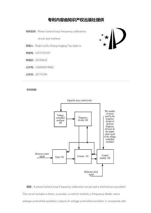
专利名称:Phase locked loop frequency calibrationcircuit and method发明人:Ruijin Liu,Xu Zhang,Jingjing Tao,Jiejie Lv申请号:US15191457申请日:20160623公开号:US09698799B2公开日:20170704专利内容由知识产权出版社提供专利附图:摘要:A phase locked loop frequency calibration circuit and a method are provided.The circuit includes a timer, a counter, a control module, a frequency divider and avoltage controlled oscillator; output of voltage controlled oscillator is connected withfirst input of frequency divider, output of frequency divider is connected with first input of counter, second input of frequency divider, first input of timer and second input of counter are respectively connected with first output of control module, third input of counter is connected with output of timer, output of counter is connected with first input of control module, a reference clock signal is respectively sent to second input of timer and second input of control module, the number of clocks used by frequency divider to perform frequency division on output clock signal of voltage controlled oscillator is sent to third input of control module.申请人:SHANGHAI EASTSOFT MICROELECTRONICS CO., LTD.地址:Shanghai CN国籍:CN代理机构:J.C. Patents更多信息请下载全文后查看。

锁相环电路原理概述By jluhong 锁相环的英文全称是Phase-Locked Loop,简称PLL。
它是由鉴相器(PD)、环路滤波器(LPF)和压控振荡器(VCO)三部分构成的一种信号相差自动调节反馈电路(环)。
PLL电路框图如下,其具体工作过程为,当输入信号Vi(t)=0时,环路滤波器的输出Vc(t)为某一固定值。
这时,压控振荡器按其固有频率fv=f0进行自由振荡。
当有频率为fi的Vi(t)输入时,Vi(t)和Vo(t)同时加到鉴相器进行鉴相。
如果二者相差不大,鉴相器输出一个与二者相位差成正比的误差电压Vd(t),再经过环路滤波器滤去Vd(t)中的高频成分,输出一个直流控制电压Vc,Vc将使压控振荡器的频率fv(和相位)发生变化,向输入信号频率fi靠拢,最后使fv= fi,环路锁定。
环路一旦进入锁定状态后,压控振荡器的输出信号与环路的输入信号(参考信号)之间只有一个固定的稳态相位差,而没有频差存在,而且当输入信号频率在捕捉带范围内变化时或相位变化时,VCO输出信号跟踪输入信号的频率和相位。
(跟踪是有条件的,即输入信号频率变化在一定范围内,否则PLL失锁)。
大家要注意,若鉴相器输入信号和VCO本振频率ωo频差很大时,鉴相器输出的差拍频率很高,则差拍频率经过环路低通滤波器被滤除了。
只有很小的分量漏加到压控振荡器的输入端。
由于控制电压太小,压控振荡器输出仍然是它的固有振荡频率ωo,整个系统输出信号基本没有发生变化,PLL失去其作用,因此要注意一个PLL电路对输入信号频率范围的限制(取决于ωo)。
鉴相器:鉴相器类型很多。
按鉴相特性分类有:正弦形鉴相器、锯齿形鉴相器、三角形鉴相器、梯形鉴相器等等;按电路性质分类有:模拟鉴相器、数字鉴相器、模拟乘法鉴相器等等。
环路滤波器可分为有源和无源二类。
压控振荡器的类别很多,常用的有LC压控振荡器,RC压控振荡器,晶体压控振荡器(VCXO)在锁相环中压控振荡器实现压控主要采用如下两种方法:直接改变决定振荡频率的振荡回路元件(如C、或R)的数值;控制多谐振荡器中定时元件的充放电流或电压。

fll frequency locked loop 结构-回复Frequency Locked Loop (FLL)是一种电子电路技术,用于以高精度地锁定输入信号的频率到内部参考频率。
在本文中,我们将深入探讨FLL结构,从基本概念到实际应用一步一步回答。
让我们开始吧!第一部分:FLL的基础知识FLL是一种反馈控制系统,通过调整VCO的频率来与输入信号的频率保持同步。
FLL主要由3个基本组件组成:一个相位比较器(Phase Comparator,PC),一个低通滤波器(Low-Pass Filter,LPF)和一个压控振荡器(Voltage Controlled Oscillator,VCO)。
PC负责比较输入信号和VCO输出信号的相位差,LPF用于滤除比较器的高频噪声,VCO则产生一个输出信号。
这三个组件构成了FLL的基本反馈环路。
第二部分:FLL的工作原理FLL的工作原理可以简化为如下几个步骤:1. 初始化:开始时,VCO的频率被设置为一个初始值,并且FLL没有锁定到输入信号的频率。
2. 相位比较:相位比较器(PC)将输入信号和VCO输出信号进行相位比较,产生一个相位差信号。
3. 相位误差检测和滤波:LPF接收PC输出信号,将高频噪声滤除,并产生一个稳定的、与相位误差成正比的电压信号。
4. 频率控制:产生的电压信号被用作VCO的控制信号,通过调整VCO频率来减小相位误差。
5. 锁定:随着VCO频率的逐渐调整,相位误差逐渐减小,并最终FLL锁定到输入信号的频率。
第三部分:FLL的应用FLL具有广泛的应用领域,下面是一些常见的应用:1. 载波恢复:在通信系统中,FLL用于恢复和跟踪接收信号的载波频率。
2. 频率合成器:FLL可以用于生成稳定的参考频率,以供其他系统使用。
3. 时钟同步:FLL可以用于同步系统中不同部件的时钟频率,确保它们保持同步。
4. 频率测量:FLL可以用于测量输入信号的频率,同时还可以提供相位差信息。

adisimpll锁相环设计过程锁相环(Phase-Locked Loop,PLL)是一种常用于时钟和信号恢复的电子电路。
它可以将输入信号的频率、相位和幅度与参考信号进行比较,然后通过调整其内部振荡器的频率和相位来保持与参考信号的同步。
在现代电子系统中,锁相环已成为许多应用的核心部件,例如通信系统、数据转换和数字信号处理等。
锁相环的设计过程通常包括以下几个主要步骤:1.确定锁相环的规格要求:首先需要确定系统的特定需求,包括输入和输出信号的频率范围、带宽、相位噪声要求以及抖动限制等。
这些规格要求将直接影响锁相环的设计参数和性能。
2.选择合适的锁相环架构:根据系统的特定需求,选择适合的锁相环架构。
常见的锁相环架构包括基于电压控制振荡器(Voltage-Controlled Oscillator,VCO)的基本锁相环、带自由运行振荡器(Free-Running Oscillator)的环-环(Ring-Oscillator)锁相环和数字控制振荡器(Digital-Controlled Oscillator,DCO)的混合锁相环等。
3.设计相位频率检测器:锁相环中的相位频率检测器(Phase-Frequency Detector,PFD)用于比较参考信号和反馈信号的相位和频率差异,并将其转化为控制信号。
常见的PFD电路包括EXOR门和带有多频偏的PFD等。
4.设计环路滤波器:设计环路滤波器用于平稳化锁相环的控制信号。
环路滤波器通常采用低通滤波器结构,能够滤除高频噪声和不稳定性。
5.设计振荡器:根据系统的频率范围和性能要求,设计合适的振荡器。
常见的VCO设计包括压控晶体振荡器(Voltage-Controlled Crystal Oscillator,VCXO)和频率可调振荡器(Voltage-Controlled Oscillator,VCO)。
6.设计控制电路:根据锁相环的设计需求,设计合适的控制电路。

fll frequency locked loop 结构-回复Frequency Locked Loop (FLL) 是一种控制系统,其结构可以用来锁定输出频率与参考频率同步。
FLL广泛应用于通信系统、电子设备和其他需要频率同步的领域。
接下来,本文将详细介绍FLL的结构和其工作原理。
1. 引言在许多领域,如高频通信、无线电接收器和数字信号处理中,频率同步是至关重要的。
频率同步是指将输出信号的频率与参考频率保持稳定和同步。
FLL可以通过组合锁相环(PLL)和频率比较器实现这一目标。
在接下来的篇章中,我们将深入探讨FLL的结构和运行机制。
2. FLL结构FLL的主要组成部分包括相位锁定环(PLL)、频率比较器和控制环路。
PLL是FLL的核心部分,它接收参考频率信号和输出频率信号,并根据比较结果来调整输出频率。
频率比较器用于比较参考频率和输出频率的差异,并输出一个误差信号。
控制环路通过根据误差信号来调整PLL的参数,从而使输出频率逐渐与参考频率同步。
3. FLL工作原理当参考频率信号进入FLL系统时,它与输出频率信号进行比较。
如果两者的频率差异很小,频率比较器输出的误差信号将趋近于零,表示两者已经同步。
然而,如果存在频率偏差,频率比较器将输出一个非零的误差信号。
这个误差信号将被送入控制环路,通过调整PLL器件的参数来减小频率偏差。
4. PLL的作用相位锁定环(PLL)是FLL的关键组件之一。
它由相位比较器、低通滤波器和电压控制振荡器(VCO)组成。
相位比较器用于比较参考频率信号和输出频率信号的相位差,然后将误差信号输出给低通滤波器。
低通滤波器通过滤除高频噪声,只保留误差信号的直流成分。
最后,VCO根据低通滤波器输出的电压信号来调整输出频率。
5. 控制环路的功能控制环路是FLL系统中的关键组成部分。
它根据频率比较器输出的误差信号来调整PLL的参数,以使输出频率趋向于参考频率。
控制环路可以通过改变PLL的增益、频率或相位来实现这一目标。

pll锁相环工作原理
PLL(Phase Locked Loop):为锁相回路或锁相环,用来统一整合时钟信号,使高频器件正常工作,如内存的存取资料等。
PLL用于振荡器中的反馈技术。
许多电子设备要正常工作,通常需要外部的输入信号与内部的振荡信号同步。
一般的晶振由于工艺与成本原因,做不到很高的频率,而在需要高频应用时,由相应的器件VCO,实现转成高频,但并不稳定,故利用锁相环路就可以实现稳定且高频的时钟信号。
锁相环路是一种反馈控制电路,简称锁相环(PLL,Phase-Locked Loop)。
锁相环的特点是:利用外部输入的参考信号控制环路内部振荡信号的频率和相位。
因锁相环可以实现输出信号频率对输入信号频率的自动跟踪,所以锁相环通常用于闭环跟踪电路。
锁相环在工作的过程中,当输出信号的频率与输入信号的频率相等时,输出电压与输入电压保持固定的相位差值,即输出电压与输入电压的相位被锁住,这就是锁相环名称的由来。
锁相环通常由鉴相器(PD,Phase Detector)、环路滤波器(LF,Loop Filter)和压控振荡器(VCO,Voltage Controlled Oscillator)三部分组成。
锁相环中的鉴相器又称为相位比较器,它的作用是检测输入信号和输出信号的相位差,并将检测出的相位差信号转换成uD(t)电压信号输出,该信号经低通滤波器滤波后形成压控振荡器的控制电压uC(t),对振荡器输出信号的频率实施控制。

Phase locked loop锁相回路Phase-locked loop锁相回路2010-04-27 23:12Phase-locked loop"PLL"redirects here.For the chemical substance polylysine,see polylysine;for the Rubik's Cube Permutation of Last Layer,see Fridrich Method;for the spinal ligament,see Posterior longitudinal ligament.A phase-locked loop or phase lock loop(PLL)is acontrol system that generates asignal that has afixed relation to the phase of a"reference"signal.A phase-locked loop circuit responds to both the frequency and the phase of the input signals,automatically raising or lowering the frequency of acontrolled oscillator until it is matched to the reference in both frequency and phase.A phase-locked loop is an example of acontrol system using negative feedback.Phase-locked loops are widely used inradio,telecommunications,computers and other electronicapplications.They may generate stable frequencies,recover asignal from anoisy communication channel,or distribute clock timing pulses indigital logic designs such as microprocessors.Since asingle integrated circuit can provide acomplete phase-locked-loop building block,the technique is widely used in modern electronic devices,with output frequencies from afraction of ahertz up to ma ny gigahertz.Analogy Tuning astring on aguitar can be compared to the operation of aphase-locked ing atuning fork or pitchpipe to provide areference frequency,the tension of the string is adjusted up or down until the beat frequency is inaudible.This indicates that the tuningfork and guitar are vibrating at the same frequency.If we imagine the guitar could be tuned perfectly to the reference tuning fork frequencyso that the string moved in exact step with the arm of the tuningfork,and maintained that relationship,the guitar string would be said to be in phase-lock with the fork.A phase-locked loops maintains its output signal in afixed phase relationship to the input signal.Structure and function Phase-locked loop mechanisms may be implemented as either analog or digital circuits.Both implementations use the same basic structure.Block diagram of aPLLBoth analog and digital PLL circuits include three basic elements:a variable electronic oscillator,anda feedback path(which oft en includes afrequency divider).Digital phase-locked loop(DPLL)A digital phase-locked loop operates similarly to an analog phase-locked loop,but is implemented entirely using digital circuits.In place of avoltage-controlled oscillator(VCO),a DPLL uses local reference clock and avariable dividing counter under digital control to create the equivalent oscillator function.DPLLs are easier to design and implement,and are less sensitive to voltage noise than analog PLLs,however they typically suffer from higher phase noise due to the quantization error of using anon-analog oscillator.For this reason digital phase locked loops are not well-suited to synthesizing higher frequencies or handling high frequency reference signals.DPLLs are sometimes used for data recovery.Analog phase-locked loop Basic design Phase-locked loop block diagramA phase detector compares two input signals and produces an error signal which is proportional to their phase difference.The error signal is then low-pass filtere dand used to drive avoltage-controlledoscillator(VCO)which creates an output frequency.The output frequency isfed through afrequency divider back to the input of the system,producing anegative feedback loop.If the output frequency drifts,the error signal will increase,driving the VCO frequency in the opposite direction so as to reduce the error.Thus the output is locked to the frequency at the other input.This input is called the reference and is often derived from acrystal oscillator,which is very stable in frequency.Analog phase locked loops are generally built of aphase detector,low pass filter and voltage-controlled oscillator(VCO)placed in anegative feedback closed-loop configuration.There may be afrequency divider in the feedback path or in the reference path,or both,in order to make the PLL's output signal frequency an integer multiple of the reference.A non integer multiple of the reference frequency can be created by replacing the simple divide-by-N counter in the feedback path with aprogrammable pulse swallowing counter.This technique is usually referred to as afractional-N synthesizer or fractional-N PLL.The oscillator generates aperiodic output signal.Assume thatinitially the oscillator is at nearly the same frequency as the reference signal.Then,if the phase from the oscillator falls behind that of the reference,the phase detector changes the control voltage of the oscillator,so that it speeds up.Likewise,if the phase creeps ahead of the reference,the phase detector changes the control voltage to slow down the oscillator.Since initially the oscillator may be far from the reference frequency,practical phase detectors may also respond to frequency differences,so as to increase the lock-in range of allowable inputs.The block commonly called alow pass filter generally has twodistinct functions.The primary function is to determine loop dynamics,also called"stability".This is how the loop responds to disturbances,such aschanges in the reference frequenc y,changes of the feedback divider,or at mon considerations are the range over which the loop can achieve lock(pull-in range or lock range),how fast the loop achieves lock(lock time or lock-up time)and overshoot(damping).Depending on the application,this may require one or more of the following:a simple proportion(gain or attenuation),an integral(low pass filter)and/or derivative(high pass filter).Loop parameters commonly examined for this are the loop's gain margin and phase mon concepts in Control Theory are used to design this function and are covered in the Control system section.The second common consideration is limiting the amount of reference frequency energy(ripple)appearing at the phase detector output that is then applied to the VCO control input.This frequency modulates the VCO and produces FM sidebands commonly called"reference spurious".The low pass characteristic of this block can be used to attenuate thisenergy,but at times aband reject"notch"ma yalso be needed.The design of this block can be dominated by either of these considerations,or can be acomplex process juggling the interactions of the two.Depending on the application,either the output of the controlled oscillator,or the control signal to the oscillator,provides the useful output of the PLL system.It should also be noted that the feedback is not limited to afrequency divider.This element can be other elements such as afrequency multiplier,or amixer.The multiplier will make the VCO output asub-multiple(rather than amultiple)of the reference frequency.A mixer can translate the VFO frequency by afixed offset.It may also be acombination of these.An example being adivider following amixer;this allows thedivider to operate at amuch lower frequency than the VCO without aloss in loop gain.。


Xilinx PLL原理Xilinx是一家全球领先的可编程逻辑器件(FPGA)和可编程系统集成电路(SoC)供应商。
他们的产品广泛应用于各个行业的电子设备中。
其中,PLL (Phase-Locked Loop,锁相环)是Xilinx芯片中的一个重要模块,它在时钟生成和信号处理中发挥着关键作用。
PLL是一种闭环控制系统,其基本原理是通过比较输入参考信号与反馈信号的相位差,并根据相位差产生的误差信号去调节输出信号的频率和相位,最终使两个信号达到同步。
Xilinx的PLL模块通常由相位频率检测器(PFD)、锁相环滤波器(Loop Filter)、电压控制振荡器(VCO)和分频器(Divider)组成。
首先,PFD会比较参考信号和反馈信号的相位差,并输出一个误差信号。
这个误差信号会经过Loop Filter的滤波,产生一个用于控制VCO频率的调节电压。
VCO会根据这个调节电压产生一个相位和频率可调的输出信号。
最后,分频器将VCO输出的信号进行分频,得到最终的输出信号。
通过调节PFD、Loop Filter和VCO的参数,可以实现PLL的多种工作模式,如锁定模式、捕获模式和跟踪模式。
锁定模式是PLL在稳定状态下工作,此时输入和输出信号相位和频率保持同步。
捕获模式用于快速将输出信号锁定到输入信号,对于输入信号发生频率变化时,PLL可以迅速跟随。
跟踪模式用于输出信号与输入信号的相位差小于设定阈值时,可以对输出信号进行微调,以保持相位同步。
Xilinx的PLL模块具有高度可调性和灵活性,用户可以根据具体应用的要求进行参数配置和调节。
它广泛应用于通信系统、数据中心、高性能计算、电视广播等领域,为各类电子设备提供稳定、准确的时钟源和信号处理功能。
总之,Xilinx PLL模块是Xilinx芯片中的一个重要组成部分,可以实现时钟生成和信号处理的关键功能。
其基本原理是利用锁相环闭环控制的方式将输入信号与输出信号同步,通过调节参数实现不同的工作模式,提供高度可调性和灵活性。

Digital Phase Locked Loops (文档可以直接使用,也可根据实际需要修改使用,可编辑欢迎下载)Digital Phase Locked LoopsMike DeLong13 May 2004TopicThe topic for this technical paper will be FPGA implementation of digital phased locked loops.ObjectiveThe objective of this paper is to explore the history, functionality, uses and FPGA implementation of digital phase locked loops.BackgroundPhase locked loops were first written about but not implemented in the early 1930’s by a French engineer named de Bellescize. In 1932 a group of British engineers started developing a receiver ba sed upon de Bellescize’s paper that would be simpler than the superheterodyne receiver that was the best available at the time. Their simple designe included a local oscillator, a mixer and an audio amplifier. When the input signal and the local oscillator were mixed at the same phase and frequency the original audio was reproduced from its modulated form. The design was very clever but had its drawbacks. Reception after a period of time became difficult due to frequency drift of the local oscillator. Their solution to this problem incorporated a phase detector comparing the input frequency to the frequency of the local oscillator. The phase detector would output a differential voltage that was fed back into the local oscillator keeping it at the correct frequency. This technique was the same technique that was developed for electronic servo control systems at the time. This was the first iteration in the evolution of the phase locked loop (PLL).Generally considered better than the superheterodyne receiver, the new phase locked loop receiver did not see widespread adoption due to the fact that cost of the PLLoutweighed it advantages. With the development of the integrated circuit, the PLL became available in low cost IC packages. This would drive the cost down and allow the PLL to be adopted in applications outside of specialized situations where the advantages outweighed the cost.In the 1940’s the PLL started seeing widespread use in horizontal and vertical sweep oscillators in television sets. Since then it has been adopted in AM and FM demodulators, FSK decoders, motor speed controls and just about anything that involves a constant frequency that needs to be tracked.Types of Phased Lock LoopsBefore detailed discussion of the FPGA implementation of the PLL can be explored, the different types of phase locked loops need to be identified. There are basically three types of phase locked loops, the PLL, DPLL and ADPLL.First is the PLL. This is basically the original design wrote about in the early ‘30s by de Bellescize. It consists of all analog components and was the standard loop for many years.The next type of loop is the DPLL or the digital phase locked loop. This new version of the PLL was developed in the 1970’s and contained bo th analog and digital parts. On most of these type of phase locked loops, the phase detector was digital and the oscillator and loop filter on the back end was analog.The ADPLL or all digital phased locked loop came along a few years after the DPLL and was an implementation of the PLL with all digital components. Since the FPGA is an exclusively digital device, the type of device that will be researched in this paper will be the ADPLL.Phase Locked Loop BasicsAny phase locked loop must have three basic components, the phase detector, the loop filter and the voltage-controlled oscillator. The diagram below shows the basic setup for the PLL.The components will differ depending on the chosen type of PLL.The phase comparator portion of the loop compares the signal generated inside of the phase locked loop to the received signal. In an analog PLL the comparator is simply a multiplier. The output from the phase comparator will consist of a frequency component at twice the intended locking frequency and an offset component equaling the sine of the phase difference between the two signals.The low pass filter in a PLL filters out the unwanted double frequency component which contains no useful information. The constant phase offset is then passed on to the voltage-controlled oscillator setting it to and keeping it at the correct frequency.The ADPLL works differently but based upon the same concept. For a digital phase locked loop, the input signal is some type of bit stream. The bit stream can have a variety of sources including an analog to digital converter or a regular bit steam with which the receiver must synchronize. Further Operation of the ADPLL will be discussed in the next section.All Digital Phase Locked Loop Design and ImplementationIn the previous section, the operation of a classic analog phase locked loop was discussed. And as stated before, operation has the same concept but works differently. The three main parts of the phase locked loop are still present in the ADPLL but they are designed and constructed differently due to the fact that the signals that they deal with are different and a FPGA is digital. The input to the ADPLL is a digital stream normally from an analog to digital converter or a clock.In this section, the individual components of the ADPLL will be broken down into their rudimentary components (i.e. counters, control bits, registers). These are the types of components that can but implemented on FPGA’s therefore this section will be about ADPLL loop design and FPGA implementation.The first stage of the ADPLL is the phase detector as it was for the PLL. In the case of the ADPLL the phase detector consists of either an EXOR gate or an edge triggered phase detector. The EXOR type is simply an EXOR logic gate.Below is representation of this kind of gate.This type of detector locks itself 90 degree behind the phase of the input signal. Two drawbacks to this type of phase detector is that it has a phase error limit of + or - 90 degrees and it is not sensitive to edges in the signal but rather the flat section. Below is an example of the “locked” state.One big advantage of this type of phase detector is its simplicity because it consists of only one logic gate.The other type of phase detector is and edge triggered device. This device is an edge triggered JK device. Its locked state is 180 degrees behind the phase of the input signal as shown below.The device is constructed as shown below.Since this device is sensitive to the edges, the clock can be eliminated. This device can be used in conjunction with a counter to output the phase error. This combination is shown below.U0NU1 MF0 JQKEnable Counter ClockIn the configuration shown above, the U0 and U1 are binary values. The MF0 is an integer multiple (M) of the reference signal F0. The counter is reset on the rising edges of U0 and is gated when the output of Q is logic 1. The output N of the counter is proportional to the phase error.The next stage of the loop is the loop filter. The loop filter that always works with the EXOR and the edge triggered phase detectors is the K counter. The K counter is shown below.CarryBarrowThis loop filter contains two separate counters both of which are counting upward. The UP/DN bit determines which counter is running at any moment. The K clock is M*F0 where M is a large integer (8, 16, 32) of the reference signal F0. The carry and borrow outputs are the most significant bits of the counters and are only high when the contents of a particular counter are greater than K/2. These values are used to control the DCO (digitally controlled oscillator). The counters are reset when the contents reach a value of K – 1.The final part of the loop is the DCO (digitally controlled oscillator). In a digital system, the oscillator is a modified counter. This part of the loop is shown on the next page.The DECR and INCR inputs are the carry and borrow outputs from the K counter respectively. This part of the loop operates in conjunction with a divide by N counter that works to slow down this accelerated clock. The 2NFc input is the center frequency of the loop (Fc) multiplied by 2N where N is the variable in the divide by N counter. The two components working together are shown below.The DECR input to the modified counter causes the take one half-cycle out. Conversely, the INCR input causes one half-cycle to be taken out of the output. The adjusted waveform is shown on the next page.This adjustment is constantly assuring that the cycles stay phased locked.All of the components discussed above are looped together forming the phase locked loop. The loop constantly adjusts the produced wave until it is in phase lock with the input wave. Below is the entire loop wired together.The phase detector component can be either discussed methods but the rest of the components are as they are shown.Uses of All Digital Phased Locked LoopsThe main uses for this type of digital phase locked loop are clock synchronization. Clocks can be match or signals with embedded clocks (such as Manchester Encoding) can be easily synchronized to. Also, any repeatable code (M-Code) could be synchronized with a modified version of this loop. For the loop to synchronize with a repeatable code, a code generator with an identical code as the unit in the receiver must be in the loop generating the internal code. The phase detector would also have to be modified to handle long strings of bits.FPGA ImplementationTechnically the topic of this paper, the FPGA implementation section will be relatively short. The sections preceding this section spoke about the individual components and their workings. Since the components have been broken down into their rudimentary parts in the previous discussion, the implementation portion becomes relatively easy. Each part of the loop will be spoken briefly about how it could be implemented.The two types of phase detectors discussed earlier in this paper have relatively simple implementations. The Exclusive-XOR gate has a simple, single gate implementation. The other type is a JK flip flop. Earlier in the paper two D flip flops and a XOR gate were used to build this device. The second part of that phase detector was a counter with a clock enable and a reset. This is an IP Core part available in the Xilinx library or a simply coded part consisting of several embedded IF-ELSIF loops.An example of this code is shown below.IF (reset = ‘1’) THENCount <= 0;ELSEIF (clk_en = ‘1’) THENCount <= Count + 1;ELSENULL;END IF;END IF:The second part of this loop is the K Counter (loop filter). This part consists of two reset able, clock enabled counters. The implementation for both of these counters is the same as the count discussed above except that the reset is based on a maximum value and both counters must be reset simultaneously.The next part of this loop is the DCO (digitally controlled oscillator). In this loop, it is simply a fast running clock that is modified by adding and deleting half cycles. This could be done with a section of code or a modified counter made to respond to the INCR and DECR bits.The last part of this loop is the divide by N counter. This is a simple counter made to switch its output logic level after N clock cycles.It can be seen that the FPGA implementation of a device like the one described in this paper could be relatively easily built. Once the individual parts are analyzed and broken down, it can be seen how to build them in a digital system.Further StudiesAn interesting research topic to branch off of this paper would be an all digital phase lock loop that locks to analog signals. The loop in this research paper synchronizes only digital type signals. An analog signal could be taken through the analog to digital converter and locked to in the loop before being retranslated through the digital to analogconverter back to analog. All of the analog math in the analog phase lock loop could be translated to discrete math and done in an FPGA.ConclusionA digital phase locked loop can have many uses. In spread spectrum, the code or clock synchronization is an important step in the decoding process. If the data bits or clock bits are out of phase then the decoded bits could be decoded incorrectly. Also, if the decoder tries to decode the bits away from the center of the bits then slight variations could cause the decoder to decode the wrong bit. The loop could also be used to synchronize to a repeatable code. This could be important if the dispreading code needed synchronized to the input.BibliographyTroha, Donald, G. “Digital Phase-Locked Loop Design Using SN54/74LS297.”TI Application Notes 5 May 200 ://focus.ti /lit/an/sdla005b/sdla005b.pdf Digital Phase Locked Loop. 5 May 2004 :// /users/gorry/course/phy-pages/dpll.htmlVan Roon, Tony. Phase-Locked Loops. 5 May 2004uoguelph.ca/~antoon/gadgets/pll/pll.html。

专利名称:PHASE-LOCKED LOOP DEVICE 发明人:TAKIMOTO HIDEKI申请号:JP592489申请日:19890117公开号:JPH02188086A公开日:19900724专利内容由知识产权出版社提供摘要:PURPOSE:To follow up even the sudden phase shift of an input video signal instantaneously by performing feedback control over an oscillator which detects the phase difference between the color burst and clock pulses in a PCM video signal directly and generates clock pulses according to the detection result, and drawing the phase back. CONSTITUTION:A 2nd latch circuit 12 synchronizes a burst flag 52 with a modulating subcarrier 55 to obtain pulses, which are used by a 1st latch circuit 11 for holding to obtain a phase error signal 56; and the signal is reconverted by a D/A converter 13 into an analog signal, which is fed back to a crystal oscillator 14. Further, a variable length shift register 17 and a variable delay circuit 15 are controlled through, a data selector 18 with a part where there is no color burst. Therefore, when an input video signal 51 shifts in phase abruptly, a phase error is detected with a color burst right after the abrupt shift, the variable length shift register 14 drawn back the phase in clock units, and the variable delay circuit 15 performs phase drawing-back operation in one clock cycle.申请人:NEC CORP更多信息请下载全文后查看。

Digital Phase Locked LoopDesign and LayoutDali Wang Fan Yang12/21/2001Contents1. Intoduction11.1Project Overview11.2Objective Of The Project21.3Table Listing Of Specifications21.3.1 The Design Specifications31.3.2The Test Specification31.4Table Of Macros41.5Table Of PinOuts51.6 Known Limitations Of Current Design52. Circuit Design 52.1 Components Description 52.1.1Phase And Frequency Detector 52.1.2Loop Filter 62.1.3 Voltage Controlled Oscillator62.2Discussion Of Tradeoffs72.3Description Of Schematics 72.3.1 Phase And Frequency Detector Schematics 72.3.2 Loop Filter Schematics 82.3.3 Voltage Controlled Oscillator Schematics 83. Circuit Performance93.1 Schematics Simulation Results 93.1.1Results For Some Important Components (Other Than Macros)93.1.2Results For Large Macros 113.1.3Entire Circuit 193.2 Discussion Of Results 234. Physical Design 254.1Description Of Components 254.2Layout Considerations 254.3Description Of Physical Layout 254.3.1Phase And Frequency Detector 254.3.2Loop Filter 26本页已使用福昕阅读器进行编辑。

fll frequency locked loop 结构-回复FLL(Frequency Locked Loop)是一种广泛应用于通信系统和信号处理中的频率解调技术。
它的工作原理基于负反馈控制理论,通过将输出信号的频率与参考信号的频率相对比,以实现对输入信号频率的稳定和精确解调。
FLL结构是实现频率锁定环的具体架构。
在一个FLL结构中,主要包括相位检测器、环路滤波器、环路增益和振荡器。
下面将详细介绍FLL各个组成部分的原理和功能,以及它们如何相互作用来实现频率锁定环。
第一个组成部分是相位检测器,它的功能是衡量输出信号的相位与参考信号的相位之间的差异。
常见的相位检测器有两种类型:环形相位检测器和非环形相位检测器。
环形相位检测器是频率锁定环中最常见的相位检测器类型。
它是由比较器构成的闭环环路,其中包含一个正反馈路径来控制环路增益。
环形相位检测器通过比较输入信号和参考信号的相位差异来产生一个误差信号,并将其输入到环路滤波器中。
环路滤波器是频率锁定环中的第二个组成部分,它的作用是对误差信号进行滤波和平滑,以消除高频噪声和不稳定性。
环路滤波器通常采用低通滤波器的形式,通过选择合适的截止频率来实现对频率锁定环的响应速度和稳定性的平衡。
环路增益是频率锁定环的第三个组成部分,它的作用是增加或减小环路的增益,以控制频率锁定的速度和精确度。
环路增益决定了频率锁定环的稳态精确度,较高的环路增益可以实现更快的锁定速度,但也会引入更多的相位噪声和振荡。
最后一个组成部分是振荡器,它的作用是产生输出信号。
在频率锁定环中,振荡器的频率是由误差信号和环路增益共同决定的。
当误差信号为零时,振荡器的频率与参考信号的频率相匹配,并保持锁定状态。
如果误差信号不为零,环路将调整振荡器的频率,以使误差信号趋向于零,并实现对输入信号频率的锁定。
总结来说,FLL结构是一种通过相位检测、环路滤波、环路增益和振荡器等组成部分相互作用的频率解调技术。


fll frequency locked loop 结构-回复什么是频率锁定环路(Frequency Locked Loop)?频率锁定环路(FLL)是一种电子系统,用于锁定输入信号的频率并产生与输入信号同步的输出频率。
FLL可以在各种应用领域中使用,例如通信系统、无线电设备和音频处理,它能够确保系统中的不同部件或设备之间相互同步。
FLL的结构主要包括以下组件:1. 相位比较器(Phase Comparator):用于比较输入信号和参考信号的相位差异,并产生一个相位误差信号。
2. 低通滤波器(Low-pass Filter):将相位误差信号通过低通滤波器滤除高频噪声,并产生一个平均误差信号。
3. 锁相环(Phase Locked Loop):接收平均误差信号,并通过控制自身的振荡频率来追踪并逐渐减小输入信号和参考信号之间的相位误差。
4. 除频器(Divider):将输出信号频率除以一个可选的整数倍,使其与参考信号频率相匹配。
5. 控制电压源(Voltage Controlled Oscillator, VCO):根据除频器输出的频率控制信号,调整VCO的振荡频率,以与输入信号频率相匹配。
6. 采样器(Sampler):从输入信号中采样,作为相位比较器的参考信号。
FLL的工作原理如下:1. 初始状态下,FLL的VCO振荡频率与输入信号的频率存在差异,因此相位比较器会产生一个相位误差信号。
2. 相位误差信号经过低通滤波器平均后,作为控制信号输入到VCO中。
VCO根据控制信号调整自身的振荡频率。
3.通过不断调整VCO振荡频率,FLL逐渐减小输入信号和参考信号之间的相位差异。
当相位误差为零时,FLL系统达到稳态,VCO的振荡频率与输入信号频率完全匹配。
4. 除频器可选地将输出信号频率除以一个整数倍,以匹配参考信号的频率。
这样可以使FLL适应不同的应用场景。
5. 采样器从输入信号中获取参考信号,并提供给相位比较器进行相位误差比较。

fll frequency locked loop 结构-回复FL frequency locked loop(频率锁相环)是一种常见的数字信号处理技术,用于估计和跟踪输入信号的频率。
它具有广泛的应用领域,包括通信、雷达、卫星导航和音频处理等。
FL频率锁相环的结构及原理十分复杂,需要逐步讨论才能全面理解。
首先,我们需要了解频率锁相环的基本概念。
频率锁相环是一种反馈控制系统,其目标是使输出信号的频率保持与输入信号的频率一致。
为了实现这一目标,FL频率锁相环通常由锁相环、相频检测器和低通滤波器组成。
锁相环中的本地振荡器的频率根据相频检测器的输出进行调整,通过反馈控制来保持输出信号与输入信号的频率一致。
在FL频率锁相环中,最关键的是锁相环部分。
锁相环主要包含一个参考信号源、一个相搬移器、一个相频检测器和一个控制环节。
首先,参考信号源提供一个稳定的参考信号。
然后,相搬移器将参考信号与本地振荡器的信号进行相位匹配。
相频检测器将比较相位差,并产生一个与输入信号的相位差成比例的电压或电流。
最后,控制环节根据相频检测器的输出信号调整本地振荡器的频率,以使输出信号的频率与输入信号的频率保持一致。
相频检测器在FL频率锁相环中起着至关重要的作用。
常见的相频检测器包括乘性相频检测器和求和相频检测器。
乘性相频检测器通过将输入信号与本地振荡器的信号进行相乘,产生一个与相位差成比例的电压或电流输出。
求和相频检测器通过将输入信号和本地振荡器的信号相加,产生一个与相位差成比例的电压或电流输出。
相频检测器的选择取决于具体的应用需求和系统性能要求。
一旦相频检测器的输出信号得到,需要经过低通滤波器进行平滑处理。
由于相频检测器的输出信号通常包含噪声和杂散成分,因此需要进行低通滤波以抑制这些不需要的频率成分。
低通滤波器的截止频率应根据具体应用进行选择,以平衡去除噪声和保留所需的信号频率的要求。
FL频率锁相环的性能与设计参数密切相关。
例如,锁相环的增益决定了系统的跟踪能力和稳定性,而环路带宽则决定了系统的响应速度和抗干扰能力。