
NRWS4R7M50V10X20F中文资料
- 格式:pdf
- 大小:215.37 KB
- 文档页数:2


1/6ADVANCED DATAJanuary 2003STW47NM50N-CHANNEL 500V -0.065Ω -45A TO-247MDmesh™Power MOSFET(1)I SD ≤45A,di/dt ≤400A/µs,V DD ≤V (BR)DSS ,T j ≤T JMAX.TYPICAL R DS (on)=0.065ΩHIGH dv/dt AND AVALANCHE CAPABILITIES 100%AVALANCHE TESTEDLOW INPUT CAPACITANCE AND GATE CHARGELOW GATE INPUT RESISTANCETIGHT PROCESS CONTROL AND HIGH MANUFACTURING YIELDSDESCRIPTIONThe MDmesh™is a new revolutionary MOSFET technology that associates the Multiple Drain pro-cess with the Company’s PowerMESH™horizontal layout.Theresulting product has an outstanding low on-resistance,impressively high dv/dt and excellent avalanche characteristics.The adoption of the Company’s proprietary strip technique yieldsoverall dynamic performance that is significantly better than that of similar competition’s products.APPLICATIONSThe MDmesh™family is very suitable for increasing power density of high voltage converters allowing system miniaturization and higher efficiencies.ABSOLUTE MAXIMUM RATINGS(•)Pulse width limited by safe operating areaTYPE V DSS R DS(on)R ds(on)*Q g I D STW47NM50500V<0.085Ω5.6Ω*nC45ASymbol ParameterValue Unit V DS Drain-source Voltage (V GS =0)500V V DGR Drain-gate Voltage (R GS =20k Ω)500V V GS Gate-source Voltage±30V I D Drain Current (continuous)at T C =25°C 45A I D Drain Current (continuous)at T C =100°C 28.4A I DM ( )Drain Current (pulsed)180A P TOT Total Dissipation at T C =25°C 417W Derating Factor2.08W/°C dv/dt (1)Peak Diode Recovery voltage slope 15V/ns T stg Storage Temperature–65to 150°C T jMax.Operating Junction Temperature150°CSTW47NM502/6THERMAL DATAAVALANCHE CHARACTERISTICSELECTRICAL CHARACTERISTICS (T CASE =25°C UNLESS OTHERWISE SPECIFIED)OFFON (1)DYNAMIC1.Pulsed:Pulse duration =300µs,duty cycle 1.5%.2.C oss eq.is defined as a constant equivalent capacitance giving the same charging time as C oss when V DS increases from 0to 80%V DSS .Rthj-case Thermal Resistance Junction-case Max 0.3°C/W Rthj-ambThermal Resistance Junction-ambientMax30°C/W T lMaximum Lead Temperature For Soldering Purpose300°CSymbol ParameterMax ValueUnit I AR Avalanche Current,Repetitive or Not-Repetitive (pulse width limited by T j max)20A E ASSingle Pulse Avalanche Energy(starting T j =25°C,I D =I AR ,V DD =35V)810mJSymbol ParameterTest ConditionsMin.Typ.Max.Unit V (BR)DSS Drain-sourceBreakdown Voltage I D =250µA,V GS =0500V I DSS Zero Gate VoltageDrain Current (V GS =0)V DS =Max Rating10µA V DS =Max Rating,T C =125°C 100µA I GSSGate-body Leakage Current (V DS =0)V GS =±30V±100nASymbol ParameterTest ConditionsMin.Typ.Max.Unit V GS(th)Gate Threshold Voltage V DS =V GS ,I D =250µA 345V R DS(on)Static Drain-source On ResistanceV GS =10V,I D =22.5A0.0650.085ΩSymbol ParameterTest ConditionsMin.Typ.Max.Unit g fs (1)Forward Transconductance V DS >I D(on)x R DS(on)max,I D =22.5A20S C iss Input Capacitance V DS =25V,f =1MHz,V GS =03700pF C oss Output Capacitance 610pF C rss Reverse Transfer Capacitance 50pF C oss eq.(2)Equivalent Output CapacitanceV GS =0V,V DS =0V to 400V 325pF R GGate Input Resistancef=1MHz Gate DC Bias =0Test Signal Level =20mV Open Drain1.7Ω3/6STW47NM50ELECTRICAL CHARACTERISTICS (CONTINUED)SWITCHING ONSWITCHING OFFSOURCE DRAIN DIODENote: 1.Pulsed:Pulse duration =300µs,duty cycle 1.5%.2.Pulse width limited by safe operating area.Symbol ParameterTest ConditionsMin.Typ.Max.Unit t d(on)Turn-on Delay Time V DD =250V,I D =22.5A R G =4.7ΩV GS =10V (see test circuit,Figure 3)40ns t r Rise Time 35ns Q g Total Gate Charge V DD =400V,I D =45A,V GS =10V87117nC Q gs Gate-Source Charge 23nC Q gdGate-Drain Charge42nCSymbol ParameterTest ConditionsMin.Typ.Max.Unit t r(Voff)Off-voltage Rise TimeV DD =400V,I D =45A,R G =4.7Ω,V GS =10V (see test circuit,Figure 5)18ns t f Fall Time 23ns t cCross-over Time44nsSymbol ParameterTest ConditionsMin.Typ.Max.Unit I SD Source-drain Current 45A I SDM (2)Source-drain Current (pulsed)180A V SD (1)Forward On Voltage I SD =45A,V GS =0 1.5V t rr Q rr I RRM Reverse Recovery Time Reverse Recovery Charge Reverse Recovery Current I SD =40A,di/dt =100A/µs,V DD =100V,T j =25°C (see test circuit,Figure 5)5207.830ns µC A t rr Q rr I RRMReverse Recovery Time Reverse Recovery Charge Reverse Recovery CurrentI SD =40A,di/dt =100A/µs,V DD =100V,T j =150°C (see test circuit,Figure 5)68011.233ns µC ASTW47NM504/6Fig.5:Test Circuit For Inductive Load Switching And Diode Recovery TimesFig.4:Gate Charge test CircuitFig.2:Unclamped Inductive WaveformFig.1:Unclamped Inductive Load TestCircuitFig.3:Switching Times Test Circuit For ResistiveLoadSTW47NM505/6STW47NM506/6Information furnished is believed to be accurate and reliable. However, STMicroelectronics assumes no responsibility for the consequences of use of such information nor for any infringement of patents or other rights of third parties which may result from its use. No license is granted by implication or otherwise under any patent or patent rights of STMicroelectronics. Specifications mentioned in this publication are subject to change without notice. This publication supersedes and replaces all information previously supplied. STMicroelectronics products are not authorized for use as critical components in life support devices or systems without express written approval of STMicroelectronics.© The ST logo is a registered trademark of STMicroelectronics© 2002 STMicroelectronics - Printed in Italy - All Rights ReservedSTMicroelectronics GROUP OF COMPANIESAustralia - Brazil - Canada - China - Finland - France - Germany - Hong Kong - India - Israel - Italy - Japan - Malaysia - Malta - Morocco Singapore - Spain - Sweden - Switzerland - United Kingdom - United States.© 。
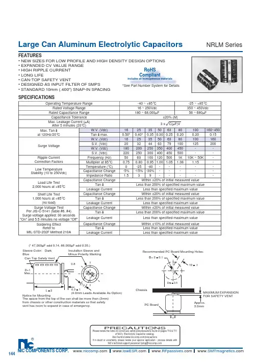
Large Can Aluminum Electrolytic CapacitorsFEATURES• NEW SIZES FOR LOW PROFILE AND HIGH DENSITY DESIGN OPTIONS • EXPANDED CV VALUE RANGE• HIGH RIPPLE CURRENT• LONG LIFE • CAN-TOP SAFETY VENT• DESIGNED AS INPUT FILTER OF SMPS • STANDARD 10mm (.400") SNAP-IN SPACING NRLM SeriesSPECIFICATIONS(* 47,000µF add 0.14, 68,000µF add 0.35.)Notice for MountingThe space from the top of the can shall be more than (3mm) from chassis or other construction materials so that safety vent has room to expand in case of emer g en c y.Sleeve Color: DarkBlueCan Top Safety VentInsulation Sleeve and Minus Polarity Marking(4.0mm Leads Available As Option)D+1Max.L ± 26.3 ± 10.810(-)(+)MAXIMUM EX P AN S IONFOR SAFETY VENT Approx. 3.0mmRecommended PC Board Mounting Holes:10 ± .1∅= 2 ± 0.1D ∅ ± 0.5ChassisPC BoardPRECAUTIONSPlease review the notes on correct use, safety and precautions found on pages T10 & T11of NIC’s Electrolytic Capacitor catalog . Operating Temperature Range-40 ~ +85°C-25 ~ +85°C Rated Voltage Range 16 ~ 250Vdc 350 ~ 450Vdc Rated Capacitance Range 180 ~ 68,000µF56 ~ 680µFCapacitance Tolerance ±20% (M)Max. Leakage Current (µA)After 5 minutes (20°C)3 x C(µF)VMax. Tan δat 120Hz/20°C W.V. (Vdc)162535506380100160~450Tan δ max.0.50*0.40*0.350.300.250.200.200.15Surge VoltageW.V. (Vdc)162535506380100160S.V. (Vdc)2032446379100125200W.V. (Vdc)180200250350400450--S.V. (Vdc)220250300400450500--Ripple CurrentCorrection Factors Frequency (Hz)50601001205001K 10K ~ 50K -Multiplier at 85°C0.750.800.95 1.00 1.05 1.08 1.15-Low TemperatureStability (10 to 250Vdc)Temperature (°C)0-25-40-----Capacitance Change-5%-15%-30%-----Impedance Ratio 1.539-----Load Life Test2,000 hours at +85°CCapacitance ChangeWithin ±20% of initial measured value Tan δLess than 200% of specifi ed maximum valueLeakage Current Less than specifi ed maximum value Shelf Life Test1,000 hours at +85°C (no load)Capacitance Change Within ±20% of initial measured value Tan δLess than 200% of specifi ed maximum valueLeakage Current Less than specifi ed maximum value Surge Voltage Test Per JIS-C-5141 (table #6, #4)Surge voltage applied: 30 seconds"On" and 5.5 minutes no voltage "Off"Capacitance Change Within ±20% of initial measured value Tan δLess than 200% of specifi ed maximum valueLeakage Current Less than specifi ed maximum value Soldering EffectRefer to MIL-STD-202F Method 210A Capacitance Change Within ±10% of initial measured valueTan δLess than specifi ed maximum value Leakage CurrentLess than specifi ed maximum valueRoHS Compliantincludes all homogeneous materials*See Part Number System for DetailsLarge Can Aluminum Electrolytic CapacitorsNRLM SeriesNRLM 222 M 50V 20X25 FRoHS compliant Case Size (mm) Voltage Rating Tolerance Code PART NUMBER SYSTEMLarge Can Aluminum Electrolytic Capacitors NRLM Series STANDARD PRODUCT LIST, CASE SIZE AND SPECIFICATIONS。
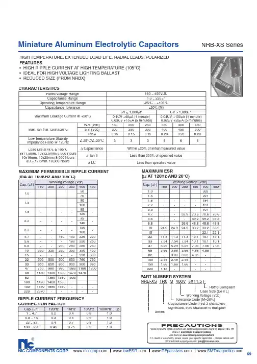

Large Can Aluminum Electrolytic CapacitorsFEATURES• NEW SIZES FOR LOW PROFILE AND HIGH DENSITY DESIGN OPTIONS • EXPANDED CV VALUE RANGE• HIGH RIPPLE CURRENT• LONG LIFE • CAN-TOP SAFETY VENT• DESIGNED AS INPUT FILTER OF SMPS • STANDARD 10mm (.400") SNAP-IN SPACING NRLM SeriesSPECIFICATIONS(* 47,000µF add 0.14, 68,000µF add 0.35.)Notice for MountingThe space from the top of the can shall be more than (3mm) from chassis or other construction materials so that safety vent has room to expand in case of emer g en c y.Sleeve Color: DarkBlueCan Top Safety VentInsulation Sleeve and Minus Polarity Marking(4.0mm Leads Available As Option)D+1Max.L ± 26.3 ± 10.810(-)(+)MAXIMUM EX P AN S IONFOR SAFETY VENT Approx. 3.0mmRecommended PC Board Mounting Holes:10 ± .1∅= 2 ± 0.1D ∅ ± 0.5ChassisPC BoardPRECAUTIONSPlease review the notes on correct use, safety and precautions found on pages T10 & T11of NIC’s Electrolytic Capacitor catalog . Operating Temperature Range-40 ~ +85°C-25 ~ +85°C Rated Voltage Range 16 ~ 250Vdc 350 ~ 450Vdc Rated Capacitance Range 180 ~ 68,000µF56 ~ 680µFCapacitance Tolerance ±20% (M)Max. Leakage Current (µA)After 5 minutes (20°C)3 x C(µF)VMax. Tan δat 120Hz/20°C W.V. (Vdc)162535506380100160~450Tan δ max.0.50*0.40*0.350.300.250.200.200.15Surge VoltageW.V. (Vdc)162535506380100160S.V. (Vdc)2032446379100125200W.V. (Vdc)180200250350400450--S.V. (Vdc)220250300400450500--Ripple CurrentCorrection Factors Frequency (Hz)50601001205001K 10K ~ 50K -Multiplier at 85°C0.750.800.95 1.00 1.05 1.08 1.15-Low TemperatureStability (10 to 250Vdc)Temperature (°C)0-25-40-----Capacitance Change-5%-15%-30%-----Impedance Ratio 1.539-----Load Life Test2,000 hours at +85°CCapacitance ChangeWithin ±20% of initial measured value Tan δLess than 200% of specifi ed maximum valueLeakage Current Less than specifi ed maximum value Shelf Life Test1,000 hours at +85°C (no load)Capacitance Change Within ±20% of initial measured value Tan δLess than 200% of specifi ed maximum valueLeakage Current Less than specifi ed maximum value Surge Voltage Test Per JIS-C-5141 (table #6, #4)Surge voltage applied: 30 seconds"On" and 5.5 minutes no voltage "Off"Capacitance Change Within ±20% of initial measured value Tan δLess than 200% of specifi ed maximum valueLeakage Current Less than specifi ed maximum value Soldering EffectRefer to MIL-STD-202F Method 210A Capacitance Change Within ±10% of initial measured valueTan δLess than specifi ed maximum value Leakage CurrentLess than specifi ed maximum valueRoHS Compliantincludes all homogeneous materials*See Part Number System for DetailsLarge Can Aluminum Electrolytic CapacitorsNRLM SeriesNRLM 222 M 50V 20X25 FRoHS compliant Case Size (mm) Voltage Rating Tolerance Code PART NUMBER SYSTEMLarge Can Aluminum Electrolytic Capacitors NRLM Series STANDARD PRODUCT LIST, CASE SIZE AND SPECIFICATIONS。