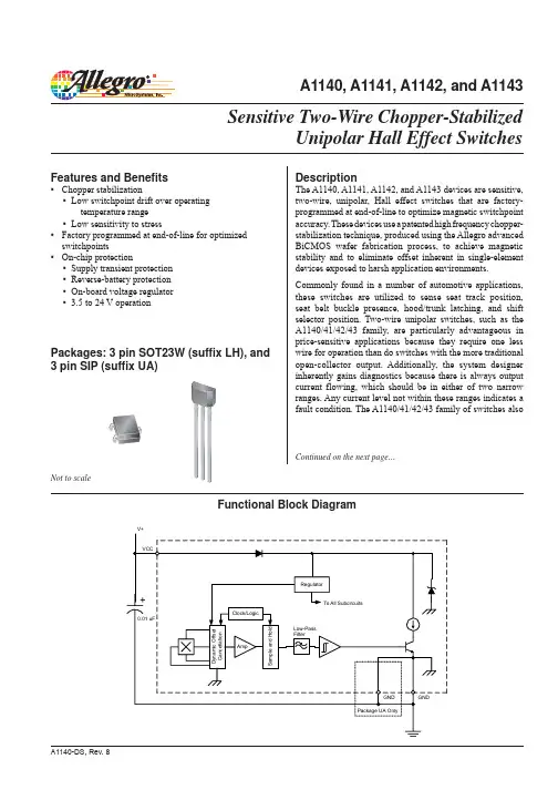
A1140, A1141, A1142, and A1143Sensitive Two-Wire Chopper-StabilizedUnipolar Hall Effect SwitchesA1140, A1141, A1142, and A1143features on-chip transient protection and a Zener clamp to protect against overvoltage conditions on the supply line.The output currents of the A1141 and A1143 switch HIGH in the presence of a south (+) polarity magnetic field of sufficient strength, and switch LOW otherwise, as in the presence of a weak field or a north (–) polarity field. The other two devices in the family (A1140 and A1142) have an opposite output: the currents switch LOW in the presence of a south-polarity magnetic field of sufficient strength,and switch HIGH otherwise. The other differences in the switches are their defined low current levels and magnetic switchpoints.All versions are offered in two package styles. The LH is a SOT-23W, miniature low-profile package for surface-mount applications. The UA is a three-lead ultramini SIP for through-hole mounting. Each package is available in a lead (Pb) free version (suffix, –T ) with 100% matte tin plated leadframe. Field-programmable versionsalso available: A1180, A1181, A1182, and A1183.Absolute Maximum RatingsCharacteristicSymbol NotesRating Units Supply Voltage V CC 28V Reverse Supply Voltage V RCC –18V Magnetic Flux DensityB Unlimited G Operating Ambient Temperature T A Range E –40 to 85ºC Range L–40 to 150ºC Maximum Junction Temperature T J (max)165ºC Storage TemperatureT stg–65 to 170ºCDescription (continued)1. VCC2. No connection3. GND1. VCC2. GND3. GNDPackage LH, 3-pin SOT Package UA, 3-pin SIPSensitive Two-Wire Chopper-StabilizedUnipolar Hall Effect SwitchesA1140, A1141, A1142, and A1143Part Number Pb-Free 1Packing 2Package Operating Ambient Temperature, T A(°C)Output Level in South (+) Field 3Supply Current at Low Output, I CC(L)(mA)A1140EUATI-T 4Yes Tape and Reel, 2000 pieces/reel Through Hole –40 to 85Low2 to 5A1140LUATI-T 4Yes Tape and Reel, 2000 pieces/reel Through Hole –40 to 150A1141EUATI-T 4Yes Tape and Reel, 2000 pieces/reel Through Hole –40 to 85HighA1141LUATI-T 4Yes Tape and Reel, 2000 pieces/reel Through Hole –40 to 150A1142ELHLT-T Yes Tape and Reel, 3000 pieces/reel Surface Mount –40 to 85Low5 to 6.9A1142EUA-T Yes Bulk Bag, 500 pieces/bag Through Hole A1142EUATI-T 4Yes Tape and Reel, 2000 pieces/reel A1142LLHLT-T Yes Tape and Reel, 3000 pieces/reel Surface Mount –40 to 150A1142LUA-T Yes Bulk Bag, 500 pieces/bag Through Hole A1142LUATI-T 4Yes Tape and Reel, 2000 pieces/reel A1143ELHLT-T Yes Tape and Reel, 3000 pieces/reel Surface Mount –40 to 85HighA1143EUA-T Yes Bulk Bag, 500 pieces/bag Through Hole A1143EUATI-T 4Yes Tape and Reel, 2000 pieces/reel A1143LLHLT-T Yes Tape and Reel, 3000 pieces/reel Surface Mount –40 to 150A1143LUA-T Yes Bulk Bag, 500 pieces/bag Through HoleA1143LUATI-T 4YesTape and Reel, 2000 pieces/reelPb-based variants are being phased out of the product line.(a) Certain variants cited in this footnote are in production but have been determined to be NOT FOR NEW DESIGN. This classification indicates that sale of this device is currently restricted to existing customer applications. The device should not be purchased for new design applications because obsolescence in the near future is probable. Samples are no longer available. Status change: May 1, 2006. These variants include A1140EUATI, A1140LUATI, A1140LUATI, A1141EUA, A1141EUATI, A1141LLHLT, A1141LUA, A1141LUATI, A1142EUATI, A1142LUATI,A1142LLHLT, A1142LUA, A1143EUATI, A1143LUA , and A1143LUATI.(b) Certain variants cited in this footnote are in production but have been determined to be LAST TIME BUY . This classification indicates that the product is obsolete and notice has been given. Sale of this device is currently restricted to existing customer applications. The device should not be purchased for new design applications because of obsolescence in the near future. Samples are no longer available. Status date change October 31, 2006. Deadline for receipt of LAST TIME BUY orders is April 27, 2007. These variants include: A1142ELHLT, A1142EUA, A1143ELHLT, A1143EUA, and A1143LLHLT.2Contact Allegro for additional packing options.3South (+) magnetic fields must be of sufficient strength.4Some restrictions may apply to certain types of sales. Contact Allegro for details.5The sensors listed in this footnote are available only in limited distribution. Interested customers should contact the appropriate sales person or field application engineer for more information on availability. These variants include: A1140ELHLT-T, A1140EUA-T, A1140LLHLT-T, A1140LUA-T, A1141ELHLT-T, A1141EUA-T, A1141LLHLT-T, and A1141LUA-T.Product Selection GuideSensitive Two-Wire Chopper-StabilizedUnipolar Hall Effect SwitchesA1140, A1141, A1142, and A1143ELECTRICAL CHARACTERISTICS over the operating voltage and temperature ranges, unless otherwise specifiedCharacteristicSymbol Test ConditionsMin.Typ.Max.Units Supply Voltage 1V CC 3.5–24V Supply Current 2I CC(L)B>B OP for A1140; B<B RP for A1141 2–5mA B>B OP for A1142; B<B RP for A1143 5-– 6.9mA I CC(H)B>B OP for A1141, A1143B<B RP for A1140, A114212-–17mA Reverse Supply Current I RCCV RCC = –18 V –––1.6mA Supply Zener Clamp Voltage V ZSUPPLY I CC = I CC(L)(max) + 3 mA; T A = 25°C 28–40V Supply Zener Clamp Current I ZSUPPLY V ZSUPPLY = 28 V––I CC(L)(max) + 3 mAmA Output Slew Rate 3di/dt Capacitance of the oscilloscope performing the measurement = 20 pF–36–mA/μs Chopping Frequency f C –200–kHz Power-On Time 3t on C BYPASS = 0.01 μF––25μs Power-On State 5,6POSt < t on ; V CC slew rate > 25 mV/μs–HIGH––1V CCrepresents the generated voltage between the VCC pin and the GND pin.2Relative values of B use the algebraic convention, where positive values indicate south magnetic polarity, and negative values indicate north magneticpolarity; therefore greater B values indicate a stronger south polarity field (or a weaker north polarity field, if present).3Measured without bypass capacitor between VCC and GND. Use of a bypass capacitor results in slower current change. 3Measured with and without bypass capacitor of 0.01 μF. Adding a larger bypass capacitor causes longer Power-On Time.5POS is defined as true only with a VCC slew rate of 25 mV/ μs or greater. Operation with a V CC slew rate less than 25 mV / μs can permanently harm device performance.6POS is undefined for t > t on or B RP < B < B OP.MAGNETIC CHARACTERISTICS over the operating voltage and temperature ranges, unless otherwise specifiedCharacteristicSymbol Test ConditionsMin.Typ.*Max.Units Operate PointB OPA1140, A1142I CC = I CC(L) 5080110GA1141, A1143I CC = I CC(H) Release Point B RP A1140, A1142I CC = I CC(H) 4565105G A1141, A1143I CC = I CC(L) HysteresisB HYSB HYS = B OP – B RP51530G*Typical data are for initial design estimations only, and assume optimum manufacturing and application conditions, such as T A = 25°C and V CC = 12 V.Performance may vary for individual units, within the specified maximum and minimum limits.Sensitive Two-Wire Chopper-StabilizedUnipolar Hall Effect SwitchesA1140, A1141, A1142, and A1143Characteristic DataSensitive Two-Wire Chopper-StabilizedUnipolar Hall Effect SwitchesA1140, A1141, A1142, and A1143THERMAL CHARACTERISTICS may require derating at maximum conditions, see application informationCharacteristicSymbolTest Conditions*Value Units Package Thermal ResistanceR θJAPackage LH, 1-layer PCB with copper limited to solder pads 228ºC/W Package LH, 2-layer PCB with 0.463 in.2 of copper area each side connected by thermal vias110ºC/W Package UA, 1-layer PCB with copper limited to solder pads165ºC/W*Additional thermal information available on Allegro Web site.6789234510111213141516171819202122232425M a x i m u m A l l o w a b l e V C C (V )Power Derating CurveV CC(min)V CC(max)100200300400500600700800900100011001200130014001500160017001800190020406080100120140160180Temperature (°C)P o w e r D i s s i p a t i o n ,P D (m W )Power Dissipation versus Ambient TemperatureSensitive Two-Wire Chopper-StabilizedUnipolar Hall Effect SwitchesA1140, A1141, A1142, and A1143Functional DescriptionHYS I CC(H)I C CI CC(L)I+(A) A1140, A1142HYSI CC(H)I C CI CC(L)I+(B) A1141, A1143OperationThe output, I CC , of the A1140 and A1142 devices switch low after the magnetic field at the Hall sensor exceeds the operate point threshold, B OP . When the magnetic field is reduced to below the release point threshold, B RP , the device output goes high. The differences between the magnetic operate and release point is called the hysteresis of the device, B HYS . This built-in hysteresis allows clean switching of the output even in the presence of external mechanical vibration and electrical noise. The A1141 and A1143 devices switch with opposite polarity for similar B OP and B RP values, in comparison to the A1140 and A1142 (see figure 1).Figure 1. Alternative switching behaviors are available in the A114x device family. On the horizontal axis, the B+ direction indicates increasing south polarity magnetic field strength, and the B– direction indicates decreasing south polarity field strength (including the case of increasing north polarity).Sensitive Two-Wire Chopper-StabilizedUnipolar Hall Effect SwitchesA1140, A1141, A1142, and A1143Chopper Stabilization TechniqueWhen using Hall-effect technology, a limiting factor for switchpoint accuracy is the small signal voltage developed across the Hall element. This voltage is disproportionally small relative to the offset that can be produced at the output of the Hall sensor. This makes it difficult to process the signal while maintaining an accurate, reliable output over the specified oper-ating temperature and voltage ranges.Chopper stabilization is a unique approach used to minimize Hall offset on the chip. The patented Allegro technique, namely Dynamic Quadrature Offset Cancellation, removes key sources of the output drift induced by thermal and mechanical stresses. This offset reduction technique is based on a signal modulation-demodulation process. The undesired offset signal is separated from the magnetic field-induced signal in the frequency domain, through modulation. The subsequent demodulation acts as a modulation process for the offset, causing the magnetic field-induced signal to recover its original spectrum at baseband, while the dc offset becomes a high-frequency signal. The magnetic-sourced signal then can pass through a low-pass filter, while the modulated dc offset is suppressed. This configuration is illus-trated in figure 2.The chopper stabilization technique uses a 200 kHz highfrequency clock. For demodulation process, a sample and hold technique is used, where the sampling is performed at twice the chopper frequency (400 kHz). This high-frequency operation allows a greater sampling rate, which results in higher accuracy and faster signal-processing capability. This approach desensi-tizes the chip to the effects of thermal and mechanical stresses, and produces devices that have extremely stable quiescent Hall output voltages and precise recoverability after temperature cycling. This technique is made possible through the use of a BiCMOS process, which allows the use of low-offset, low-noise amplifiers in combination with high-density logic integration and sample-and-hold circuits.The repeatability of magnetic field-induced switching is affected slightly by a chopper technique. However, the Allegro high-frequency chopping approach minimizes the affect of jitter and makes it imperceptible in most applications. Applications that are more likely to be sensitive to such degradation are those requiring precise sensing of alternating magnetic fields; forexample, speed sensing of ring-magnet targets. For such applica-tions, Allegro recommends its digital sensor families with lower sensitivity to jitter. For more information on those devices, contact your Allegro sales representative.Figure 2. Chopper stabilization circuit (Dynamic Quadrature Offset Cancellation)HallSensitive Two-Wire Chopper-StabilizedUnipolar Hall Effect SwitchesA1140, A1141, A1142, and A1143Application InformationFor additional general application information, visit the Allegro Web site at www. .0.01μFUA Onlyseparation 5mmBYP Figure 3. Typical application circuitTypical Application CircuitThe A114x family of devices must be protected by an external bypass capacitor, C BYP , connected between the supply, VCC, and the ground, GND, of the device. C BYP reduces both external noise and the noise generated by the chopper-stabilization func-tion. As shown in figure 3, a 0.01 μF capacitor is typical.Installation of C BYP must ensure that the traces that connect it to the A114x pins are no greater than 5 mm in length.All high-frequency interferences conducted along the supply lines are passed directly to the load through C BYP , and it serves only to protect the A114x internal circuitry. As a result, the load ECU (electronic control unit) must have sufficient protection, other than C BYP , installed in parallel with the A114x.A series resistor on the supply side, RS (not shown), in combina-tion with C BYP , creates a filter for EMI pulses.When determining the minimum V CC requirement of the A114x device, the voltage drops across R S and the ECU sense resistor, R SENSE , must be taken into consideration. The typical value for R SENSE is approximately 100 Ω.Sensitive Two-Wire Chopper-StabilizedUnipolar Hall Effect SwitchesA1140, A1141, A1142, and A1143Power DeratingThe device must be operated below the maximum junctiontemperature of the device, T J(max). Under certain combinations of peak conditions, reliable operation may require derating sup-plied power or improving the heat dissipation properties of the application. This section presents a procedure for correlating factors affecting operating T J . (Thermal data is also available on the Allegro MicroSystems Web site.)The Package Thermal Resistance, R θJA , is a figure of merit sum-marizing the ability of the application and the device to dissipate heat from the junction (die), through all paths to the ambient air. Its primary component is the Effective Thermal Conductivity, K, of the printed circuit board, including adjacent devices and traces. Radiation from the die through the device case, R θJC , is relatively small component of R θJA . Ambient air temperature, T A , and air motion are significant external factors, damped by overmolding.The effect of varying power levels (Power Dissipation, P D ), can be estimated. The following formulas represent the fundamental relationships used to estimate T J , at P D . P D = V IN × I IN (1)ΔT = P D × R θJA (2)T J = T A + ΔT(3)For example, given common conditions such as: T A = 25°C,V CC = 12 V, I CC = 4 mA, and R θJA = 140 °C/W, then: P D = V CC × I CC = 12 V × 4 mA = 48 mW ΔT = P D × R θJA = 48 mW × 140 °C/W = 7°CT J = T A + ΔT = 25°C + 7°C = 32°CA worst-case estimate, P D(max), represents the maximum allow-able power level (V CC(max), I CC(max)), without exceeding T J(max), at a selected R θJA and T A .Example : Reliability for V CC at T A = 150°C, package UA, using minimum-K PCB.Observe the worst-case ratings for the device, specifically: R θJA = 165°C/W, T J(max) = 165°C, V CC(max) = 24 V , and I CC(max) = 17 mA.Calculate the maximum allowable power level, P D(max). First, invert equation 3:ΔT max = T J(max) – T A = 165 °C – 150 °C = 15 °CThis provides the allowable increase to T J resulting from internal power dissipation. Then, invert equation 2:P D(max) = ΔT max ÷ R θJA = 15°C ÷ 165 °C/W = 91 mW Finally, invert equation 1 with respect to voltage: V CC(est) = P D(max) ÷ I CC(max) = 91 mW ÷ 17 mA = 5 V The result indicates that, at T A , the application and device can dissipate adequate amounts of heat at voltages ≤V CC(est).Compare V CC(est) to V CC(max). If V CC(est) ≤ V CC(max), then reli-able operation between V CC(est) and V CC(max) requires enhanced R θJA . If V CC(est) ≥ V CC(max), then operation between V CC(est) and V CC(max) is reliable under these conditions.Sensitive Two-Wire Chopper-StabilizedUnipolar Hall Effect SwitchesA1140, A1141, A1142, and A1143Device Qualification ProgramEMC (Electromagnetic Compatibility) RequirementsTest NameReference Specification ESD – Human Body Model AEC-Q100-002ESD – Machine Model AEC-Q100-003Conducted Transients ISO 7637-2Direct RF Injection ISO 11452-7Bulk Current Injection ISO 11452-4TEM CellISO 11452-3Contact Allegro for information.Contact your local representative for EMC results.Sensitive Two-Wire Chopper-StabilizedUnipolar Hall Effect SwitchesA1140, A1141, A1142, and A1143Package LH, 3-Pin; (SOT-23W)Sensitive Two-Wire Chopper-StabilizedUnipolar Hall Effect SwitchesA1140, A1141, A1142, and A1143The products described herein are manufactured under one or more of the following U.S. patents: 5,045,920; 5,264,783; 5,442,283; 5,389,889; 5,581,179; 5,517,112; 5,619,137; 5,621,319; 5,650,719; 5,686,894; 5,694,038; 5,729,130; 5,917,320; and other patents pending.Allegro MicroSystems, Inc. reserves the right to make, from time to time, such de p ar t ures from the detail spec i f i c a t ions as may be required to permit improvements in the per f or m ance, reliability, or manufacturability of its products. Before placing an order, the user is cautioned to verify that the information being relied upon is current.Allegro products are not authorized for use as critical components in life-support devices or sys t ems without express written approval. The in f or m a t ion in c lud e d herein is believed to be ac c u r ate and reliable. How e v e r, Allegro MicroSystems, Inc. assumes no re s pon s i b il i t y for its use; nor for any in f ringe m ent of patents or other rights of third parties which may result from its use. Copyright © 2004, 2006 Allegro MicroSystems, Inc.Package UA, 3-Pin SIP。