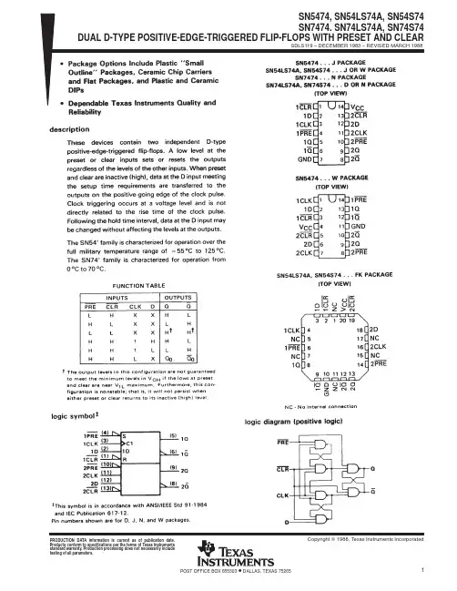
CY5474FCT157T中文资料
- 格式:pdf
- 大小:65.91 KB
- 文档页数:6
Quad 2-Input MultiplexerCY54/74FCT157TSCCS014 - May 1994 - Revised February 2000Data sheet acquired from Cypress Semiconductor Corporation.Data sheet modified to remove devices not offered.Copyright © 2000, T exas Instruments IncorporatedFeatures•Function, pinout, and drive compatible with FCT and F logic•FCT-C speed at 4.3 ns max. (Com’l),FCT-A speed at 5.0 ns max. (Com’l)•Reduced V OH (typically = 3.3V) versions of equivalent FCT functions•Edge-rate control circuitry for significantly improved noise characteristics •Power-off disable feature •Matched rise and fall times•Fully compatible with TTL input and output logic levels •ESD > 2000V•Extended commercial range of −40˚C to +85˚C •Sink current 64 mA (Com’l),32 mA (Mil)Source current 32 mA (Com’l),12 mA (Mil)Functional DescriptionThe FCT157T is a quad two-input multiplexer that selects four bits of data from two sources under the control of a common data Select input (S).The Enable input (E)is Active LOW.When (E)is HIGH,all of the outputs (Y)are forced LOW regardless of all other input conditions.Moving data from two groups of registers to four common output buses is a common use of the FCT157T.The state of the Select input determines the particular register from which the data comes.It can also be used as a function generator.The device is useful for implementing highly irregular logic by generating any four of the sixteen different functions of two variables with one variable common.The FCT157T is a logic implementation of a four-pole,two-position switch where the position of the switch is determined by the logic levels supplied to the Select input.The outputs are designed with a power-off disable feature to allow for live insertion of boards.LogicBlock Diagram,FCT157TPin Configurations12345678V CC GNDTop ViewFCT157T 4891011127651516171832120131419I 1bI 0bY a I 1dI 0cI 0dNC N C N C V CC EGND Y dTop ViewSOIC/QSOP I 1aLCC NC 161514131211109Y a SI 1a I 0a I 1d I 0d E I 0aSI 1aI 0bI 1bI 0cI 1cI 0dI 1dY aY bY cY dY b I 1b I 0b I 1c I 0c Y d Y cS I 0a Y b I 1cY c EFCT157T–1Y aSI 1a I 0a I 1dI 0d Y bI 1b I 0b I 1c I 0c Y cY dE FCT157TFCT157TLogic SymbolMaximum Ratings [2,3](Above which the useful life may be impaired.For user guide-lines, not tested.)Storage T emperature .....................................−65°C to +150°C Ambient T emperature withPower Applied ..................................................−65°C to +135°C Supply Voltage to Ground Potential ..................−0.5V to +7.0V DC Input Voltage .................................................−0.5V to +7.0V DC Output Voltage ..............................................−0.5V to +7.0V DC Output Current (Maximum Sink Current/Pin)......120 mAPower Dissipation..........................................................0.5W Static Discharge Voltage............................................>2001V (per MIL-STD-883, Method 3015)Pin DescriptionName DescriptionS Common Select Input E Enable Inputs (Active LOW)I 0Data Inputs from Source 0I 1Data Inputs from Source 1YNon-Inverted OutputFunction Table [1]InputsOutputsE S I 0I 1Y H X X X L L H X L L L H X H H L L L X L LLHXHOperating RangeRange Range Ambient Temperature V CC Commercial All −40°C to +85°C 5V ± 5%Military [4]All−55°C to +125°C5V ± 10%Electrical Characteristics Over the Operating RangeParameter DescriptionTest ConditionsMin.Typ.[5]Max.Unit V OHOutput HIGH VoltageV CC =Min., I OH =−32 mA Com’l 2.0V V CC =Min., I OH =−15 mA Com’l 2.4 3.3V V CC =Min., I OH =−12 mAMil 2.43.3V V OL Output LOW Voltage V CC =Min., I OL =64 mA Com’l 0.30.55V V CC =Min., I OL =32 mAMil0.30.55V V IH Input HIGH Voltage 2.0V V IL Input LOW Voltage 0.8V V H Hysteresis [6]All inputs0.2V V IK Input Clamp Diode Voltage V CC =Min., I IN =−18 mA −0.7−1.2V I I Input HIGH Current V CC =Max., V IN =V CC 5µA I IH Input HIGH Current V CC =Max., V IN =2.7V ±1µA I IL Input LOW CurrentV CC =Max., V IN =0.5V ±1µA I OZH Off State HIGH-Level Output CurrentV CC = Max., V OUT = 2.7V 10µA I OZL Off State LOW-Level Output CurrentV CC =Max., V OUT = 0.5V −10µA I OS Output Short Circuit Current [7]V CC =Max., V OUT =0.0V −60−120−225mA I OFFPower-Off DisableV CC =0V , V OUT =4.5V±1µANote:1.H = HIGH Voltage Level. L = LOW Voltage Level. X = Don’t Care2.Unless otherwise noted, these limits are over the operating free-air temperature range.3.Unused inputs must always be connected to an appropriate logic voltage level, preferably either V CC or ground.4.T A is the “instant on” case temperature.5.Typical values are at V CC =5.0V , T A =+25˚C ambient.6.This parameter is specified but not tested.7.Not more than one output should be shorted at a time.Duration of short should not exceed one second.The use of high-speed test apparatus and/or sampleand hold techniques are preferable in order to minimize internal chip heating and more accurately reflect operational values.Otherwise prolonged shorting of a high output may raise the chip temperature well above normal and thereby cause invalid readings in other parametric tests.In any sequence of parameter tests, I OS tests should be performed last.Capacitance[6]Parameter Description Typ.[5]Max.Unit C IN Input Capacitance510pFC OUT Output Capacitance912pF Power Supply CharacteristicsParameter Description Test Conditions Typ.[5]Max.Unit I CC Quiescent Power Supply Current V CC=Max., V IN≤0.2V, V IN≥V CC−0.2V0.10.2mA∆I CC Quiescent Power Supply Current(TTL inputs HIGH)V CC=Max., V IN=3.4V,[8]f1=0, Outputs Open0.5 2.0mAI CCD Dynamic Power Supply Current[9]V CC=Max., One Input Toggling,50% Duty Cycle, Outputs Open,OE=GND, V IN≤0.2V or V IN≥V CC−0.2V0.060.12mA/MHzI C Total Power Supply Current[10]V CC=Max., 50% Duty Cycle,Outputs Open,One Input Toggling at f1=10 MHz,OE=GND, V IN≤0.2V or V IN≥V CC−0.2V0.7 1.4mAV CC=Max., 50% Duty Cycle,Outputs Open,One Input Toggling at f1=10 MHz,OE=GND, V IN=3.4V or V IN=GND1.02.4mAV CC=Max., 50% Duty Cycle,Outputs Open,Four Bits Toggling at f1=2.5 MHz,OE=GND, V IN≤0.2V or V IN≥V CC−0.2V0.7 1.4[11]mAV CC=Max., 50% Duty Cycle,Outputs Open,Four Bits Toggling at f1=2.5 MHz,OE=GND, V IN=3.4V or V IN=GND1.7 5.4[11]mANotes:8.Per TTL driven input (V IN=3.4V); all other inputs at V CC or GND.9.This parameter is not directly testable, but is derived for use in Total Power Supply calculations.10.I C=I QUIESCENT + I INPUTS+ I DYNAMICI C=I CC+∆I CC D H N T+I CCD(f0/2 + f1N1)I CC=Quiescent Current with CMOS input levels∆I CC=Power Supply Current for a TTL HIGH input (V IN=3.4V)D H=Duty Cycle for TTL inputs HIGHN T=Number of TTL inputs at D HI CCD=Dynamic Current caused by an input transition pair(HLH or LHL)f0=Clock frequency for registered devices, otherwise zerof1=Input signal frequencyN1=Number of inputs changing at f1All currents are in milliamps and all frequencies are in megahertz.11.Values for these conditions are examples of the I CC formula. These limits are specified but not tested.Document #: 38−00288-CSwitching Characteristics Over the Operating RangeParameter Description FCT157T FCT157ATFCT157CT Unit Fig.No.[13}CommercialMilitaryCommercial Commercial Min.[12]Max.Min.[12]Max.Min.[12]Max.Min.[12]Max.t PLH t PHL Propagation Delay I to Y1.5 6.0 1.5 5.8 1.5 5.0 1.5 4.3ns 1, 3t PLH t PHL Propagation Delay E to Y1.510.5 1.57.4 1.5 6.0 1.5 4.8ns 1, 5t PLH t PHLPropagation Delay S to Y1.510.51.58.11.57.01.55.2ns1, 3Ordering InformationSpeed (ns)Ordering CodePackage Name Package TypeOperating Range 4.3CY74FCT157CTQCT Q116-Lead (150-Mil) QSOP CommercialCY74FCT157CTSOC/SOCT S116-Lead (300-Mil) Molded SOIC 5.0CY74FCT157ATQCT Q116-Lead (150-Mil) QSOP Commercial CY74FCT157ATSOC/SOCT S116-Lead (300-Mil) Molded SOIC 5.8CY54FCT157ATLMBL6120-Pin Square Leadless Chip CarrierMilitary Note:12.Minimum limits are specified but not tested on Propagation Delays.13.See “Parameter Measurement Information” in the General Information SectionPackage Diagrams20-Pin Square Leadless Chip Carrier L61MIL −STD −1835 C −2APackage Diagrams(continued)16-Lead Quarter Size Outline Q116-Lead Molded SOIC S1IMPORTANT NOTICETexas Instruments and its subsidiaries (TI) reserve the right to make changes to their products or to discontinue any product or service without notice, and advise customers to obtain the latest version of relevant information to verify, before placing orders, that information being relied on is current and complete. All products are sold subject to the terms and conditions of sale supplied at the time of order acknowledgement, including those pertaining to warranty, patent infringement, and limitation of liability.TI warrants performance of its semiconductor products to the specifications applicable at the time of sale in accordance with TI’s standard warranty. Testing and other quality control techniques are utilized to the extent TI deems necessary to support this warranty. Specific testing of all parameters of each device is not necessarily performed, except those mandated by government requirements.CERTAIN APPLICATIONS USING SEMICONDUCTOR PRODUCTS MAY INVOLVE POTENTIAL RISKS OF DEATH, PERSONAL INJURY, OR SEVERE PROPERTY OR ENVIRONMENTAL DAMAGE (“CRITICAL APPLICATIONS”). TI SEMICONDUCTOR PRODUCTS ARE NOT DESIGNED, AUTHORIZED, OR WARRANTED TO BE SUITABLE FOR USE IN LIFE-SUPPORT DEVICES OR SYSTEMS OR OTHER CRITICAL APPLICATIONS. INCLUSION OF TI PRODUCTS IN SUCH APPLICATIONS IS UNDERSTOOD TO BE FULLY AT THE CUSTOMER’S RISK.In order to minimize risks associated with the customer’s applications, adequate design and operating safeguards must be provided by the customer to minimize inherent or procedural hazards.TI assumes no liability for applications assistance or customer product design. TI does not warrant or represent that any license, either express or implied, is granted under any patent right, copyright, mask work right, or other intellectual property right of TI covering or relating to any combination, machine, or process in which such semiconductor products or services might be or are used. TI’s publication of information regarding any third party’s products or services does not constitute TI’s approval, warranty or endorsement thereof.Copyright © 2000, Texas Instruments Incorporated。