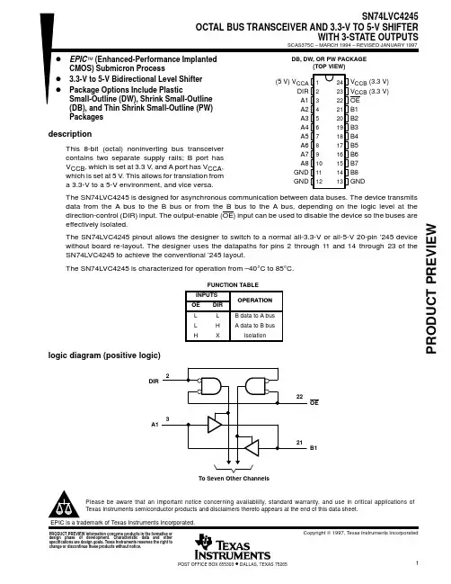
SN74CBTLV3125中文资料
- 格式:pdf
- 大小:290.77 KB
- 文档页数:12
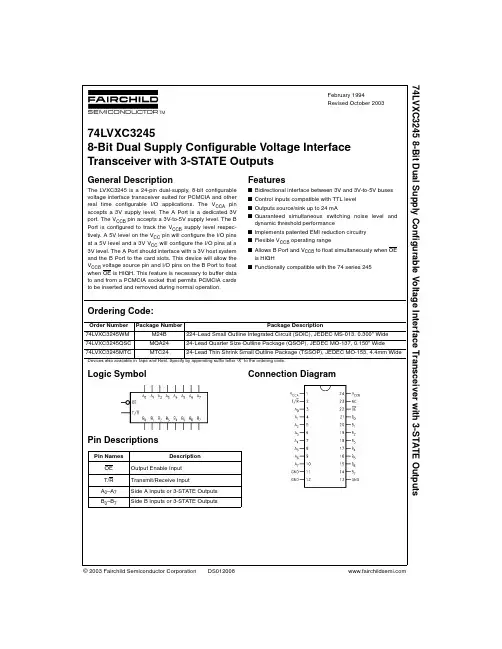
SN74CBTLV3125LOWĆVOLTAGE QUADRUPLE FET BUS SWITCH
SCDS037J − DECEMBER 1997 − REVISED OCTOBER 2003
1POST OFFICE BOX 655303 • DALLAS, TEXAS 75265POST OFFICE BOX 1443 • HOUSTON, TEXAS 77251−1443DStandard ’125-Type PinoutD5-Ω Switch Connection Between Two PortsDRail-to-Rail Switching on Data I/O PortsDIoff Supports Partial-Power-Down ModeOperationDLatch-Up Performance Exceeds 100 mA PerJESD 78, Class II
D, DGV, NS, OR PW PACKAGE(TOP VIEW)
NC − No internal connectionDBQ PACKAGE(TOP VIEW)
12345678161514131211109NC1OE1A1B2OE2A2BGNDVCC4OE4A4B3OE3A3BNC12345671413121110981OE1A1B2OE2A2BGNDVCC4OE4A4B3OE3A3BRGY PACKAGE(TOP VIEW)
114
78234561312111094OE4A4B3OE3A1A1B2OE2A2B1OE
3BV
GNDCC
description/ordering informationThe SN74CBTLV3125 quadruple FET bus switch features independent line switches. Each switch is disabledwhen the associated output-enable (OE) input is high.This device is fully specified for partial-power-down applications using Ioff. The Ioff feature ensures thatdamaging current will not backflow through the device when it is powered down. The device has isolation duringpower off.To ensure the high-impedance state during power up or power down, OE should be tied to VCC through a pullupresistor; the minimum value of the resistor is determined by the current-sinking capability of the driver.ORDERING INFORMATIONTAPACKAGE†ORDERABLEPART NUMBERTOP-SIDEMARKINGQFN − RGYTape and reelSN74CBTLV3125RGYRCL125TubeSN74CBTLV3125DSOIC − DTape and reelSN74CBTLV3125DRCBTLV3125°°SOP − NSTape and reelSN74CBTLV3125NSRCBTLV3125−40C to 85CSSOP (QSOP) − DBQTape and reelSN74CBTLV3125DBQRCL125TSSOP − PWTape and reelSN74CBTLV3125PWRCL125TVSOP − DGVTape and reelSN74CBTLV3125DGVRCL125†Package drawings, standard packing quantities, thermal data, symbolization, and PCB design guidelinesare available at www.ti.com/sc/package.
Copyright 2003, Texas Instruments IncorporatedPRODUCTION DATA information is current as of publication date.Products conform to specifications per the terms of Texas Instrumentsstandard warranty. Production processing does not necessarily includetesting of all parameters.Please be aware that an important notice concerning availability, standard warranty, and use in critical applications ofTexasInstruments semiconductor products and disclaimers thereto appears at the end of this data sheet.元器件交易网www.cecb2b.comSN74CBTLV3125LOWĆVOLTAGE QUADRUPLE FET BUS SWITCH
SCDS037J − DECEMBER 1997 − REVISED OCTOBER 2003
2POST OFFICE BOX 655303 • DALLAS, TEXAS 75265POST OFFICE BOX 1443 • HOUSTON, TEXAS 77251−1443FUNCTION TABLE(each bus switch)INPUTOEFUNCTIONLA port = B portHDisconnectlogic diagram (positive logic)
1A
1OESW1B
2A
2OESW2B
3A
3OESW3B
4A
4OESW4B2
1
5
43
6
9
10
12
138
11
Pin numbers shown are for the D, DGV, NS, PW, and RGY packages.
simplified schematic, each FET switch
A
(OE)B元器件交易网www.cecb2b.comSN74CBTLV3125LOWĆVOLTAGE QUADRUPLE FET BUS SWITCH
SCDS037J − DECEMBER 1997 − REVISED OCTOBER 2003
3POST OFFICE BOX 655303 • DALLAS, TEXAS 75265POST OFFICE BOX 1443 • HOUSTON, TEXAS 77251−1443absolute maximum ratings over operating free-air temperature range (unless otherwise noted)†
Supply voltage range, VCC −0.5 V to 4.6 V. . . . . . . . . . . . . . . . . . . . . . . . . . . . . . . . . . . . . . . . . . . . . . . . . . . . . . . . . Input voltage range, VI (see Note 1) −0.5 V to 4.6 V. . . . . . . . . . . . . . . . . . . . . . . . . . . . . . . . . . . . . . . . . . . . . . . . . Continuous channel current 128 mA. . . . . . . . . . . . . . . . . . . . . . . . . . . . . . . . . . . . . . . . . . . . . . . . . . . . . . . . . . . . . . Input clamp current, IIK (VI/O < 0) −50 mA. . . . . . . . . . . . . . . . . . . . . . . . . . . . . . . . . . . . . . . . . . . . . . . . . . . . . . . . . Package thermal impedance, θJA(see Note 2):D package 86°C/W. . . . . . . . . . . . . . . . . . . . . . . . . . . . . . . . . . . (see Note 2):DBQ package 90°C/W. . . . . . . . . . . . . . . . . . . . . . . . . . . . . . . . (see Note 2):DGV package 127°C/W. . . . . . . . . . . . . . . . . . . . . . . . . . . . . . . (see Note 2):NS package 76°C/W. . . . . . . . . . . . . . . . . . . . . . . . . . . . . . . . . (see Note 2):PW package 113°C/W. . . . . . . . . . . . . . . . . . . . . . . . . . . . . . . . (see Note 3):RGY package 47°C/W. . . . . . . . . . . . . . . . . . . . . . . . . . . . . . . . Storage temperature range, Tstg −65°C to 150°C. . . . . . . . . . . . . . . . . . . . . . . . . . . . . . . . . . . . . . . . . . . . . . . . . . . †Stresses beyond those listed under “absolute maximum ratings” may cause permanent damage to the device. These are stress ratings only, andfunctional operation of the device at these or any other conditions beyond those indicated under “recommended operating conditions” is notimplied. Exposure to absolute-maximum-rated conditions for extended periods may affect device reliability.NOTES:1.The input and output negative-voltage ratings may be exceeded if the input and output clamp-current ratings are observed.2.The package thermal impedance is calculated in accordance with JESD 51-7.3.The package thermal impedance is calculated in accordance with JESD 51-5.recommended operating conditions (see Note 4)MINMAXUNITVCCSupply voltage2.33.6VVVCC = 2.3 V to 2.7 V1.7IHHigh-level control input voltageVCC = 2.7 V to 3.6 V2VVCC = 2.3 V to 2.7 V0.7VILLow-level control input voltageVCC = 2.7 V to 3.6 V0.8VTAOperating free-air temperature−4085°CNOTE 4:All unused control inputs of the device must be held at VCC or GND to ensure proper device operation. Refer to the TI application report,Implications of Slow or Floating CMOS Inputs, literature number SCBA004.元器件交易网www.cecb2b.com