
FLDL-TTL-14T中文资料
- 格式:pdf
- 大小:1.07 MB
- 文档页数:2
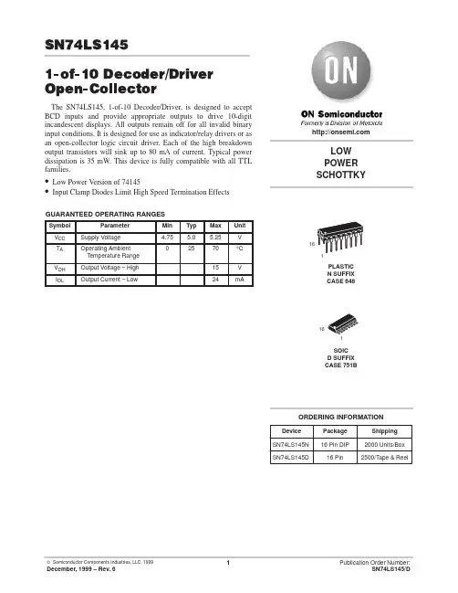
LOW POWER SCHOTTKYDevice Package Shipping SN74LS145N 16 Pin DIP 2000 Units/Box SN74LS145D16 PinSOIC D SUFFIX CASE 751B2500/T ape & ReelPLASTIC N SUFFIX CASE 648161161ON Semiconductor and are trademarks of Semiconductor Components Industries, LLC (SCILLC). SCILLC reserves the right to make changes without further notice to any products herein. SCILLC makes no warranty, representation or guarantee regarding the suitability of its products for any particular purpose, nor does SCILLC assume any liability arising out of the application or use of any product or circuit, and specifically disclaims any and all liability, including without limitation special, consequential or incidental damages. “Typical” parameters which may be provided in SCILLC data sheets and/or specifications can and do vary in different applications and actual performance may vary over time. All operating parameters, including “Typicals” must be validated for each customer application by customer’s technical experts. SCILLC does not convey any license under its patent rights nor the rights of others.SCILLC products are not designed, intended, or authorized for use as components in systems intended for surgical implant into the body, or other applications intended to support or sustain life, or for any other application in which the failure of the SCILLC product could create a situation where personal injury or death may occur. Should Buyer purchase or use SCILLC products for any such unintended or unauthorized application, Buyer shall indemnify and hold SCILLC and its officers, employees, subsidiaries, affiliates, and distributors harmless against all claims, costs, damages, and expenses, and reasonable attorney fees arising out of, directly or indirectly, any claim of personal injury or death associated with such unintended or unauthorized use, even if such claim alleges that SCILLC was negligent regarding the design or manufacture of the part. SCILLC is an Equal Opportunity/Affirmative Action Employer. PUBLICATION ORDERING INFORMATIONASIA/PACIFIC: LDC for ON Semiconductor – Asia SupportPhone:303–675–2121 (Tue–Fri 9:00am to 1:00pm, Hong Kong Time)Toll Free from Hong Kong 800–4422–3781Email: ONlit–asia@JAPAN: ON Semiconductor, Japan Customer Focus Center4–32–1 Nishi–Gotanda, Shinagawa–ku, Tokyo, Japan 141–8549Phone: 81–3–5487–8345Email: r14153@Fax Response Line:303–675–2167。
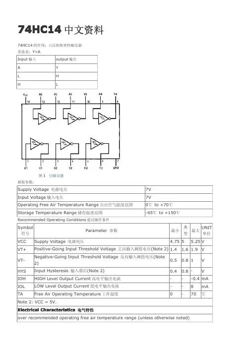
74HC14中文资料74HC14的作用:六反相斯密特触发器真值表:Y=AInput输入output输出A YL HH L图1引脚功能极限参数:Supply Voltage电源电压7VInput Voltage输入电压7VOperating Free Air Temperature Range自由空气温度范围0℃to+70℃Storage Temperature Range储存温度范围-65℃to+150℃Recommended Operating Conditions建议操作条件Symbol 符号Parameter参数最小典型最大UNIT单位VCC Supply Voltage电源电压 4.755 5.25V VT+Positive-Going Input Threshold Voltage正向输入阈值电压(Note2)1.4 1.6 1.9VVT-Negative-Going Input Threshold Voltage反向输入阈值电压(Note2)0.50.81VHYS Input Hysteresis输入滞后(Note2)0.40.8-V IOH HIGH Level Output Current高电平输出电流---0.4mA IOL LOW Level Output Current低电平输出电流--8mA TA Free Air Operating Temperature工作温度0-70℃Note2:VCC=5V.Electrical Characteristics电气特性over recommended operating free air temperature range(unless otherwise noted)Symbol 符号Parameter参数Conditions条件最小典型最大UNIT单位VI Input Clamp Voltage输入钳位电压VCC=最小,II=-18mA---1.5VVOH HIGH Level Output Voltage输出高电平电压VCC=最小,IOH=最大VIL=最大2.73.4-VVOL LOW Level输出低电平电压VCC=最小,IOL=最大-0.350.5--Output Voltage输出电压VIH=最小---V VCC=最小,IOL=4mA-0.250.4IT+Input Current at Positive-GoingThreshold正向阈值输入电流VCC=5V,VI=VT+--0.14-mAIT-Input Current at Negative-GoingThreshold反向阈值输入电流VCC=5V,VI=VT---0.18-mAII Input Current@MAX Input Voltage输入电流@最大输入电压VCC=最大,VI=7V--0.1mAIIH HIGH Level Input Current输入高电平电流VCC=最大,VI=2.7V--20μAIIL LOW Level Input Current输入低电平电流VCC=最大,VI=0.4V---0.4mAIOS Short Circuit Output Current短路输出电流VCC=最大(Note4)-20--100mAICCH Supply Current with Out puts HIGH高电平输出电源电流VCC=最大-8.616mAICCL Supply Current with Outputs LOW低电平输出电源电流VCC=最大-1221mANote3:VCC=5V,TA=25℃.Note4:Not more than one output should be shorted at a time,and the duration should not exceed one second.Switching Characteristics开关特性at VCC=5V and TA=25℃Switching Characteristics开关特性at VCC=5V and TA=25℃Symbol 符号Parameter参数RL=2kΩUNIT单位CL=15pF CL=50pF最小最大最小最大tPLH Propagation Delay Time LOW-to-HIGH Level Output低到高电平输出传递延迟时间522825nstPHL Propagation Delay Time HIGH-to-LOW Level Output高到低电平输出传递延迟时间5221033ns应用电路:图2光电藕合器接收整形电路图3方波振荡器。
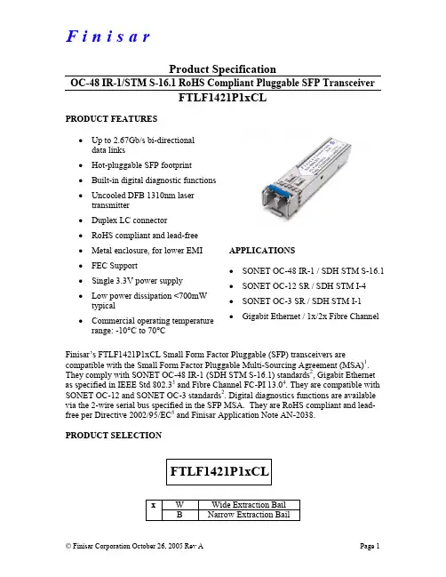

FLM1414-4FInternally Matched Power GaAs FETFujitsu recommends the following conditions for the reliable operation of GaAs FETs:1. The drain-source operating voltage (V DS ) should not exceed 10 volts.2. The forward and reverse gate currents should not exceed 16.0 and -2.2 mA respectively with gate resistance of 100Ω.G.C.P.: Gain Compression Point,S.C.L.: Single Carrier LevelFEATURES• High Output Power:P 1dB = 36.0dBm (Typ.)• High Gain:G 1dB = 6.0dB (Typ.)• High PAE:ηadd = 27% (Typ.)• Low IM 3= -46dBc@Po = 25.5dBm (Typ.)• Broad Band:14.0 ~ 14.5GHz• Impedance Matched Zin/Zout = 50Ω• Hermetically SealedDESCRIPTIONThe FLM1414-4F is a power GaAs FET that is internally matched for standard communication bands to provide optimum power and gain in a 50 ohm system.Eudyna’s stringent Quality Assurance Program assures the highest reliability and consistent performance.ηa d d (%)FLM1414-4FInternally Matched Power GaAs FETS-PARAMETERSV DS= 10V, I DS= 1100mAFREQUENCY S11S21S12S22 (MHZ)MAG ANG MAG ANG MAG ANG MAG ANG13800.479-159.9 1.883-51.6.080-54.0.459156.713900.436-178.2 1.921-70.6.084-73.1.454134.314000.388162.3 1.955-90.8.093-94.2.438112.714100.334141.1 1.990-110.4.098-115.0.43092.114200.278117.4 2.017-131.2.100-135.6.41368.914300.20988.3 2.032-151.9.110-157.1.38148.014400.16247.6 2.050-172.9.113-177.9.35324.814500.150-8.2 2.016165.3.114160.0.3070.414600.194-55.1 1.966143.4.116138.4.256-24.414700.264-89.3 1.882121.0.115117.5.216-55.4S0°S21S12FLM1414-4FInternally Matched Power GaAs FETEudyna Devices Inc. products contain gallium arsenide(GaAs) which can be hazardous to the human body and the environment. For safety, observe the following procedures:CAUTION• Do not put this product into the mouth.• Do not alter the form of this product into a gas, powder, or liquidthrough burning, crushing, or chemical processing as these by-products are dangerous to the human body if inhaled, ingested, or swallowed.• Observe government laws and company regulations when discarding this product. This product must be discarded in accordance with methods specified by applicable hazardous waste procedures.For further information please contact:Eudyna Devices USA Inc.2355 Zanker Rd.San Jose, CA 95131-1138, U.S.A.TEL:(408) 232-9500FAX:(408) 428-9111Eudyna Devices Europe Ltd.Network House Norreys DriveMaidenhead, Berkshire SL6 4FJ United KingdomTEL:+44 (0) 1628 504800FAX:+44 (0) 1628 504888Eudyna Devices Asia Pte Ltd.Hong Kong BranchRm.1101, Ocean Centre, 5 Canton Rd.Tsim Sha Tsui, Kowloon, Hong Kong TEL:+852-2377-0227FAX:+852-2377-3921Eudyna Devices Inc.Sales Division1, Kanai-cho, Sakae-kuY okohama, 244-0845, Japan TEL:+81-45-853-8156FAX:+81-45-853-8170Eudyna Devices Inc.reserves the right to change products and specifications without notice.The information does not convey any license under rights of Eudyna Devices Inc.or others.©2004 Eudyna Devices USA Inc.Printed in U.S.A.。