西门康可控硅介绍
- 格式:pdf
- 大小:172.88 KB
- 文档页数:8
mcr16可控硅中文参数摘要:一、可控硅简介1.可控硅的定义2.可控硅的作用二、mcr16 可控硅的参数1.额定电压2.额定电流3.控制极电压4.开关速度5.静态阻抗三、mcr16 可控硅的特性与应用1.低动态阻抗2.高电压应答速度3.应用领域四、mcr16 可控硅的注意事项1.安装与接线2.工作环境3.维护与保养正文:一、可控硅简介可控硅(Silicon Controlled Rectifier,简称SCR)是一种四层三端的半导体器件,具有电压控制的开关特性。
它主要用于交流电路中的整流、交直流转换、逆变等,从而实现对电压、电流的控制。
二、mcr16 可控硅的参数1.额定电压:mcr16 可控硅的额定电压为1600V,这意味着在正常工作条件下,其可以承受的电压范围为1600V。
2.额定电流:mcr16 可控硅的额定电流为16A,表示在1600V 的电压下,其最大可承受的电流为16A。
3.控制极电压:mcr16 可控硅的控制极电压范围为2-10V,这是控制信号所需的电压范围。
4.开关速度:mcr16 可控硅的开关速度快,响应时间一般在100ns 左右,能够满足大多数应用场景的需求。
5.静态阻抗:mcr16 可控硅的静态阻抗低,有利于减小电路中的电压降,提高整体系统的效率。
三、mcr16 可控硅的特性与应用1.低动态阻抗:mcr16 可控硅具有低动态阻抗,可以有效降低整流器、逆变器等设备的体积和重量。
2.高电压应答速度:mcr16 可控硅具有高电压应答速度,能够实现快速、精确的控制,满足高精度电力电子设备的需求。
3.应用领域:mcr16 可控硅广泛应用于工业控制、通信、家电、电源等领域,如交流调压、直流稳压、交直流变换等。
四、mcr16 可控硅的注意事项1.安装与接线:在安装和接线过程中,应确保mcr16 可控硅的引脚正确连接,避免引脚短路或接错。
2.工作环境:mcr16 可控硅应安装在干燥、通风、无腐蚀性气体的环境中,以保证其正常工作和使用寿命。
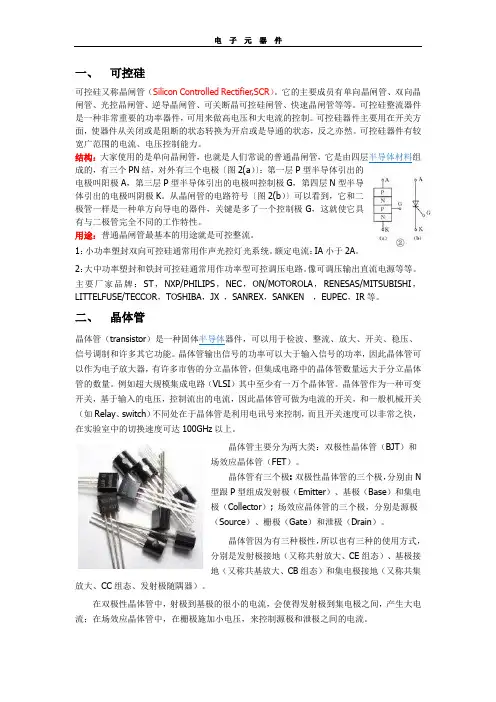
一、可控硅可控硅又称晶闸管(Silicon Controlled Rectifier,SCR)。
它的主要成员有单向晶闸管、双向晶闸管、光控晶闸管、逆导晶闸管、可关断晶可控硅闸管、快速晶闸管等等。
可控硅整流器件是一种非常重要的功率器件,可用来做高电压和大电流的控制。
可控硅器件主要用在开关方面,使器件从关闭或是阻断的状态转换为开启或是导通的状态,反之亦然。
可控硅器件有较宽广范围的电流、电压控制能力。
结构:大家使用的是单向晶闸管,也就是人们常说的普通晶闸管,它是由四层半导体材料组成的,有三个PN结,对外有三个电极〔图2(a)〕:第一层P型半导体引出的电极叫阳极A,第三层P型半导体引出的电极叫控制极G,第四层N型半导体引出的电极叫阴极K。
从晶闸管的电路符号〔图2(b)〕可以看到,它和二极管一样是一种单方向导电的器件,关键是多了一个控制极G,这就使它具有与二极管完全不同的工作特性。
用途:普通晶闸管最基本的用途就是可控整流。
1:小功率塑封双向可控硅通常用作声光控灯光系统。
额定电流:IA小于2A。
2:大中功率塑封和铁封可控硅通常用作功率型可控调压电路。
像可调压输出直流电源等等。
主要厂家品牌:ST,NXP/PHILIPS,NEC,ON/MOTOROLA,RENESAS/MITSUBISHI,LITTELFUSE/TECCOR,TOSHIBA,JX ,SANREX,SANKEN ,EUPEC,IR等。
二、晶体管晶体管(transistor)是一种固体半导体器件,可以用于检波、整流、放大、开关、稳压、信号调制和许多其它功能。
晶体管输出信号的功率可以大于输入信号的功率,因此晶体管可以作为电子放大器,有许多市售的分立晶体管,但集成电路中的晶体管数量远大于分立晶体管的数量。
例如超大规模集成电路(VLSI)其中至少有一万个晶体管。
晶体管作为一种可变开关,基于输入的电压,控制流出的电流,因此晶体管可做为电流的开关,和一般机械开关(如Relay、switch)不同处在于晶体管是利用电讯号来控制,而且开关速度可以非常之快,在实验室中的切换速度可达100GHz以上。
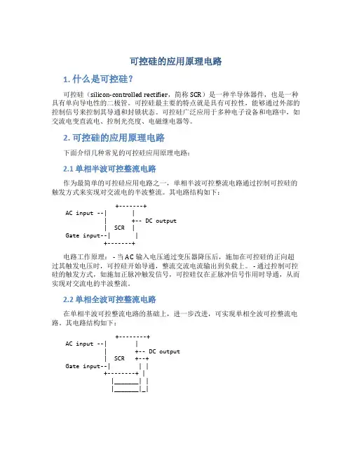
可控硅的应用原理电路1. 什么是可控硅?可控硅(silicon-controlled rectifier,简称SCR)是一种半导体器件,也是一种具有单向导电性的二极管。
可控硅最主要的特点就是具有可控性,能够通过外部的控制信号来控制其导通和封锁状态。
可控硅广泛应用于多种电子设备和电路中,如交流电变直流电、控制光亮度、电磁继电器等。
2. 可控硅的应用原理电路下面介绍几种常见的可控硅应用原理电路:2.1 单相半波可控整流电路作为最简单的可控硅应用电路之一,单相半波可控整流电路通过控制可控硅的触发方式来实现对交流电的半波整流。
其电路结构如下:+-------+AC input --| || +-- DC output| SCR |Gate input--| |+-------+电路工作原理: - 当AC输入电压通过变压器降压后,施加在可控硅的正向超过其触发电压时,可控硅开始导通,整流交流电流输出到负载上。
- 通过控制可控硅的触发方式,如施加正脉冲触发信号,可控硅仅在正脉冲信号作用时导通,从而实现对交流电的半波整流。
2.2 单相全波可控整流电路在单相半波可控整流电路的基础上,进一步改进,可实现单相全波可控整流电路。
其电路结构如下:+--------+AC input --| || +-- DC output| SCR +--+Gate input--| | |+--------+ ||_______| ||_______|_|电路工作原理: - 当AC输入电压通过变压器降压后,施加在可控硅的正向超过其触发电压时,可控硅开始导通,整流交流电流输出到负载上。
- 在正半周期内,一个可控硅导通,另一个不导通;在负半周期内,上述两个可控硅的导通状态互换。
通过交替控制两个可控硅的触发方式,可实现对交流电的全波整流。
2.3 可控硅交流电压调光电路可控硅还可用于交流电压的调光控制。
常见的应用是在家庭或公共场所的照明系统中。
可控硅象限可控硅(ControllableSilicon)是一种可控材料,是指利用电场把硅原子在它们的原子核外转移,从而改变硅材料的自由电子状态的过程。
因此,可控硅具有非常重要的应用价值,它不仅可以用于新型非易失存储器的开发,用于新型生物传感器的开发,还可以应用于新型电脑内存和芯片制造等方面。
可控硅作为一种电子材料,具有极佳的优点:比如体积小,传导能力强,成本低等。
其中比较显著的一个优势就是它的非易失性。
可控硅的一个重要特征是它的自由电子状态可以完全由电场控制,这种可控性使其成为未来电子存储技术的重要发展方向。
可控硅象限(Controllable Silicon Quadrant)是一种基于可控硅的新型电子存储技术,主要通过改变可控硅的电子态来实现存储信息的功能。
它的要点是在可控硅表面上制作出以二维网格形式排列的“象限”,并通过相应的电场对它们进行控制,使其具备存取和编辑功能,从而实现电子存储。
可控硅象限的优势在于拥有非常高的可靠性和稳定性。
它可以通过电场控制来改变自由电子状态,从而实现稳定性,在这种情况下拥有极高的可靠性。
此外,由于可控硅象限的体积小,重量轻,成本低,因此在实用性方面也占据绝对的优势,是一种有前景的新型电子存储技术。
可控硅象限的应用也在不断拓展,它在科学研究方面的应用也是非常广泛的,比如在医学集成电路、生物探测器、芯片制造、内存存储优化、芯片模拟、智能传感器、高速电路设计等都有着重要的作用。
可控硅象限是一种新颖的电子存储技术,它不仅拥有传统存储技术所不具备的可靠性,而且具有体积小、重量轻、成本低等的特点,在实用性方面也占据绝对的优势,在未来电子存储技术中将取得更大的发展和进步。
总之,可控硅象限已经成为一种新型电子存储技术,它具有稳定性、可靠性、体积小、重量轻等特点,并且有着广泛的应用价值,对学术界和工业界具有重要的意义,因此,今后将有更多实际应用和发展前景,可控硅象限必将成为电子存储技术的一部分,给我们带来更多的发展机遇。
bta416y可控硅参数摘要:一、可控硅简介1.可控硅的定义2.可控硅的分类二、bta416y 可控硅参数1.结构与特性2.电气参数a.额定电压b.额定电流c.极间耐压d.开关速度三、bta416y 可控硅应用领域1.电气控制2.电力电子3.通信设备4.家用电器四、bta416y 可控硅的优势与局限1.优势a.高效率b.快速开关c.低噪音d.长寿命2.局限a.承受电压有限b.导通电阻较大c.控制电路复杂正文:【一、可控硅简介】可控硅(Silicon Controlled Rectifier,简称SCR)是一种四层三端的半导体器件,具有电压控制的开关特性。
它有阳极(Anode,A)、阴极(Cathode,K)和控制极(Gate,G)三个端子。
通过改变控制极的电压,可以控制器件的导通与截止。
可控硅广泛应用于各种电子设备和电气控制系统中。
【二、bta416y 可控硅参数】【1.结构与特性】bta416y 可控硅采用平面结构,具有体积小、重量轻的特点。
其内部为NPN 和PNP 晶体管结构,具有高速、高效率、低噪音和长寿命等优点。
【2.电气参数】【a.额定电压】bta416y 可控硅的额定电压为1000V,表示在额定电压下可以正常工作。
【b.额定电流】bta416y 可控硅的额定电流为4A,表示在额定电压下最大可承受的电流。
【c.极间耐压】bta416y 可控硅的极间耐压为1200V,意味着在极间施加1200V 的电压时,器件不会被击穿。
【d.开关速度】bta416y 可控硅的开关速度较快,可以实现快速开关控制,响应时间短。
【三、bta416y 可控硅应用领域】【1.电气控制】bta416y 可控硅在电气控制系统中可以实现稳压、调压、交直流转换等功能,提高系统的稳定性和可靠性。
【2.电力电子】bta416y 可控硅在电力电子设备中具有广泛应用,如整流器、逆变器、变频器等,提高能源转换效率。
【3.通信设备】bta416y 可控硅在通信设备中也有广泛应用,如电源系统、充电器等,确保通信设备的稳定运行。

SH30A三相智能型可控硅控制器使用说明书上海史晖自动化设备有限公司SH30A三相智能型可控硅触发器使用说明书产品特点◆自动判别R.S.T三相相位◆自动/手动控制任意切换◆电压限制:0-100%可调◆带上电缓启动,时间可调◆负载接法不限,可设定◆LED三色灯指示运行/故障◆调压分辨率:0.2 °,线性化精度:±0.3V◆全智能三相六路宽脉冲触发电路,安全.可靠.稳定◆调压、周波调功、PWM调功,三种工作模式任意设定◆三相负载任意断一相时另两相可以继续工作一、主要技术指标:1 输入信号4~20mA DC 输 入, 接受阻抗:100 Ω ; 0~10V DC输入 ,输入阻抗450KΩ0~5V DC输入 ,输入阻抗450KΩ2 调节输出分辨力调节输出分辨力:0.2 °。
线性化精度:±0.3 V3 负载方式50Hz 三相380V AC ,中心接地或不接地可选。
4 LED状态显示灯输入指示LED灯(1支):红色:4~20mA 输入信号指示三色状态LED灯(1支):绿色,运行(有输出)黄色闪烁,停机(无输出)红绿闪烁,散热器超温报警(无输出)5 缓启动缓关断缓启动:0-120 秒可调。
首次上电或手动转自动时启动, 用于降低冷态启动的平均功率,减小对负载的冲击。
缓关断:10秒,不可调6 启动/停止开关(外接开关)R1端:CN1-3端子,RS端:CN1-7端子R1 - RS端:无电压接点输入短路:缓关断, 开路:缓启动7 一组报警输出继电器报警输出: ALM,报警接点,容量 240V AC 1A (纯阻)。
8 散热器超温保护CN3检测散热器温度信号,常闭点。
建议使用75℃常闭温度开关。
当散热器温度超过75℃时,温度开关断开,触发板急停。
若不使用温度开关,CN3两端子需短路。
9 控制方式调相控制:连续调压调功控制:阻性周波过零调功10 移相范围0~175°,星型负载(中心点接地)0~150°,三角型负载或星型负载(中心点不接地)11 驱动输出配单硅反并联式可控硅模块可变宽度脉冲:8°~120°电压:5V 电流:100mA最大(最大可触发西门康SKT1000单硅反并联)12 手自动切换可转换手动或自动调节,配10K电位器可手动调节输出功率。
bta12可控硅参数摘要:一、可控硅简介1.可控硅定义2.可控硅的作用二、bta12 可控硅参数1.结构与特点2.参数说明a.额定电压b.额定电流c.极间耐压d.开关速度e.最小触发电流三、bta12 可控硅应用领域1.电气控制2.电力电子3.工业自动化四、bta12 可控硅的优缺点1.优点a.高电压、大电流应用b.快速开关c.低导通电阻2.缺点a.控制较复杂b.存在反向恢复电流正文:【一、可控硅简介】可控硅(Silicon Controlled Rectifier,简称SCR)是一种四层三端的半导体器件,具有电压控制的开关特性。
它具有两个主电极(阳极和阴极)和一个控制极(栅极)。
当控制极施加一定的正向电压时,可控硅处于导通状态,允许电流流过;当控制极电压移除时,可控硅处于截止状态,电流不会流过。
可控硅广泛应用于各种电气控制、电力电子和工业自动化等领域。
【二、bta12 可控硅参数】bta12 是一种常用的可控硅型号,具有以下参数:1.结构与特点:bta12 可控硅采用平面结构,具有体积小、重量轻、可靠性高等特点。
2.参数说明:a.额定电压:bta12 可控硅的额定电压为1200V。
b.额定电流:bta12 可控硅的额定电流为30A。
c.极间耐压:bta12 可控硅的极间耐压为1800V。
d.开关速度:bta12 可控硅的开关速度快,响应时间一般在100ns 左右。
e.最小触发电流:bta12 可控硅的最小触发电流为10mA。
【三、bta12 可控硅应用领域】bta12 可控硅广泛应用于以下领域:1.电气控制:用于交流电机、直流电机、变频器、电源等设备的控制和保护。
2.电力电子:用于整流器、逆变器、斩波器、交流稳压器等电力电子设备。
3.工业自动化:用于自动化生产线、机器人、可编程逻辑控制器(PLC)等工业自动化系统。
【四、bta12 可控硅的优缺点】bta12 可控硅具有以下优点:1.高电压、大电流应用:bta12 可控硅具有较高的额定电压和额定电流,适用于高电压、大电流场合。
双向可控硅的相关介绍,一文讲清楚!01▶双向可控硅介绍◀双向可控硅TRIAC(Triode ACSemiconductor Switch)为三端双向可控硅开关,亦称为双向晶闸管或双向可控硅。
TRIAC为三端元件,其三端分别为T1 (第二端子或第二阳极),T 2(端子或阳极)和G(控制极)亦为一闸极控制开关,与SCR的不同点在于TRIAC无论于正向或反向电压时皆可导通,其符号构造及外型,如图1所示。
02▶双向可控硅的特性及用途◀1. 双向可控硅替的主要优点体现在:(1)大功率双向可控硅为无触点式开关,无火花、寿命长、体积小、无噪音;(2)接触器工作时,其控制回路需要消耗一定的电能,而可控硅为弱电控制,控制回路耗电微乎其微;(3)接触器控制电路中,操作者接触的器件电压都较高,不安全,而大功率双向可控硅控制电路中操作者只接触5~15V的直流低压电源,非常安全;(4)大功率双向可控硅为弱电控制强电,弱电电路更新方便,较容易设计出满足各种要求的控制电路。
2. 双向可控硅替在电路中的主要用途双向可控硅基本的用途就是可控整流。
大家熟悉的二极管整流电路属于不可控整流电路。
如果把二极管换成晶闸管,就可以构成可控整流电路。
在正弦交流电压U2的正半周期间,如果VS的控制极没有输入触发脉冲Ug,VS仍然不能导通,只有在U2处于正半周,在控制极外加触发脉冲Ug时,晶闸管被触发导通。
而只有在触发脉冲Ug到来时,负载RL上才有电压UL输出(波形图上阴影部分)。
Ug到来得早,晶闸管导通的时间就早;Ug到来得晚,晶闸管导通的时间就晚。
通过改变控制极上触发脉冲Ug到来的时间,就可以调节负载上输出电压的平均值UL(阴影部分的面积大小)。
在电工技术中,常把交流电的半个周期定为180°,称为电角度。
这样,在U2的每个正半周,从零值开始到触发脉冲到来瞬间所经历的电角度称为控制角α;在每个正半周内晶闸管导通的电角度叫导通角θ。
很明显,α和θ都是用来表示晶闸管在承受正向电压的半个周期的导通或阻断范围的。
可控硅参数符号意义可控硅(Silicon Controlled Rectifier,SCR)是一种典型的半导体器件,在电力电子领域广泛应用。
它是一种电流控制型的电子开关,可以实现电路的开关控制,广泛应用于电能控制、电流调节、频率变换和电力转换等方面。
在可控硅的参数中,有一些重要的符号和意义,下面将详细解释。
1. IGT:触发电流(Gate Trigger Current)IGT是指在开关偏置电压条件下,从控制极(Gate)流入可控硅的电流。
当IGT达到一定值时,可控硅进入导通状态。
IGT的大小与可控硅的导通灵敏度和触发电路设计有关。
IGT越小,可控硅的触发能力越强。
2. VGT:触发电压(Gate Trigger Voltage)VGT是指正常导通状态下,为使可控硅在控制极(Gate)上具有触发能力所需的电压。
当VGT达到一定值时,可控硅开始导通,只有当控制极的电压达到或超过这个值时,可控硅才能被触发。
3. IH:保持电流(Holding Current)IH是可控硅在导通状态下能够维持稳定导通所需的最小电流。
当电路中的电流小于IH时,可控硅将进入关断状态。
4. VDRM:最大反向电压(Maximum Repetitive Peak Reverse Voltage)VDRM是可控硅在关断状态下的最大允许电压。
当电路的反向电压超过VDRM时,可控硅将出现击穿现象,导致不可逆损坏。
5. IT(RMS):有效值电流(RMS On-State Current)IT(RMS)是指可控硅在导通状态下所能承受的最大有效值电流。
超过这个值,可控硅将无法承受,可能引起过热和损坏。
6. VTM:最大导通压降(Maximum On-State Voltage Drop)VTM是可控硅在导通状态下的最大导通电压降。
这个电压降是导通状态下硅芯片内部电导引起的,电流大时电压降也相应增大。
7. dV/dt:最大耐受斜率(Maximum Allowable Rate of Rise of Off-State Voltage)dV/dt是可控硅在关断状态下能够承受的最大耐受斜率。
CR6AM可控硅参数介绍1. 可控硅简介可控硅(Silicon Controlled Rectifier,SCR),也被称为晶闸管,是一种具有控制能力的半导体器件。
可控硅最早由贝尔实验室的团队在1957年研制成功,它具有双极性能,可以用作开关和增强电压效应。
可控硅常用于电力控制、电机控制、电子加热、光控制等领域。
2. CR6AM可控硅参数CR6AM是一种常见的可控硅型号,它具有以下主要参数:2.1 极限参数•电压:最大反向电压(VRRM)和最大正向电压(VRM)是可控硅能够承受的最大电压范围。
•电流:最大正向电流(IFRM)是可控硅能够连续承受的最大电流,最大阻断电流(IRRM)是可控硅处于关断状态时能够承受的最大电流。
•温度:最大结温(Tjmax)是可控硅能够承受的最高温度。
2.2 电特性可控硅的电特性描述了其在导通和关断状态下的电压和电流关系。
- 正向特性:正向压降(VF)是可控硅在导通状态下的正向电压,正向电导(Rd)描述了导通状态下的电流变化情况。
- 反向特性:反向电流(IR)是可控硅在关断状态下的反向漏电流。
2.3 控制特性•门极电流(IGT):为了将可控硅从关断状态转变为导通状态,需要施加一个足够的正向电流,该电流称为门极电流。
•电压门极电流产品(VGT):在门极电流作用下,可控硅在导通状态下的电压范围。
•关断特性:关断电流(IH)是当可控硅处于导通状态时,再次转变为关断状态所需的最小电流。
•瞬态特性:可控硅的开启时间(tq)是指从施加控制信号到可控硅导通的时间。
关断时间(trr)是指从控制信号撤离到可控硅完全关断的时间。
3. CR6AM可控硅应用CR6AM可控硅常应用于以下领域: - 电力控制:可控硅可以用来调节电压、电流,实现对电力系统的精确控制。
例如,交流调光、电力供应的无功补偿等。
- 电机控制:通过控制可控硅的导通和关断,可以实现对电机速度的调节、制动,同时也可以避免电机过载烧坏。
可控硅工作象限一、概述可控硅(SCR)是一种半导体器件,也被称为晶闸管。
它可以在某些条件下控制电流的流动,因此被广泛应用于电力电子领域。
可控硅工作象限是指可控硅在电路中正常工作的区域。
二、可控硅的基本原理可控硅由四个半导体材料构成,分别是P型半导体、N型半导体和两个金属接触层。
当一个正向电压施加在P型半导体上时,它将吸收大量的电子,并形成一个空穴区域。
同样地,当一个反向电压施加在N型半导体上时,它将吸收大量的空穴,并形成一个电子区域。
当P型和N型半导体相互连接时,它们之间会形成一个PN结。
当PN结处于正向偏置状态时,正向电流可以通过它流动,并且PN结内部没有阻力。
但是,在反向偏置状态下,PN结内部会有很高的阻力,并且几乎不允许任何电流通过。
三、可控硅工作象限1. 通态区通态区是指可控硅处于正向偏置状态时的区域。
在这个区域内,可控硅可以承受电流和电压,并且正常工作。
在通态区中,可控硅的电阻非常小,几乎为零。
2. 关断区关断区是指可控硅处于反向偏置状态时的区域。
在这个区域内,可控硅不能承受任何电流或电压。
如果在关断区施加电压或电流,它会立即烧毁。
3. 触发区触发区是指可控硅处于正向偏置状态时,在某些条件下可以转换到导通状态的区域。
在触发区中,可控硅的电阻开始变大,并且需要一个外部信号来触发它进入导通状态。
4. 饱和区饱和区是指可控硅处于导通状态时的区域。
在这个区域内,可控硅可以承受很大的电流和电压,并且保持导通状态。
在饱和区中,可控硅的电阻非常小,几乎为零。
四、触发方式1. 门极触发门极触发是最常用的一种方式。
它通过施加一个脉冲信号来激活可控硅,使其进入导通状态。
门极触发的优点是速度快、可靠性高。
2. 电流触发电流触发是通过施加一个足够大的电流来激活可控硅,使其进入导通状态。
这种方式适用于需要长时间保持导通状态的情况。
3. 光触发光触发是通过施加一个光信号来激活可控硅,使其进入导通状态。
这种方式适用于需要隔离高电压或高电流的情况。
电动车充电器输出端的可控硅一、可控硅的概念和作用可控硅(SCR)是一种半导体器件,也称为晶闸管。
它可以实现电流的控制和开关功能,常用于电力电子设备中。
在电动车充电器中,可控硅被用来控制输出端的电流和电压。
二、电动车充电器输出端的可控硅原理1. 可控硅的结构可控硅由PNP结构和NPN结构组成,具有三个引脚:阳极(A)、阴极(K)和门(G)。
PNP结构由P型半导体片、N型半导体片和P型半导体片组成;NPN结构由N型半导体片、P型半导体片和N型半导体片组成。
2. 可控硅的工作原理当可控硅的门极接受到一个正脉冲信号时,它就会进入导通状态。
在这个状态下,从阳极到阴极之间的电流可以被完全地控制。
当门极信号结束时,可控硅将自动断开。
3. 电动车充电器输出端的可控硅工作原理在充电器输出端,通过对可控硅进行触发信号来控制输出电流和电压。
当充电器需要输出电流时,可控硅被触发进入导通状态,从而使电流通过输出端口。
当充电器需要停止输出电流时,可控硅被关闭。
三、可控硅在电动车充电器中的应用1. 控制充电器的输出功率在使用充电器为电动车充电时,可控硅可以帮助调整输出功率。
通过改变可控硅的触发角度和工作周期,可以调整输出端口的平均功率和有效值。
2. 控制充电器的输出电压在使用充电器为不同类型的车辆充电时,需要调整输出端口的电压。
通过改变可控硅的触发角度和工作周期,可以实现对输出端口的直流或交流信号进行调整。
3. 控制充电器的输出稳定性在使用充电器为不同类型的车辆进行快速或慢速充电时,需要保持稳定性。
通过使用可控硅来实现对输出端口信号波形进行调整,可以提高稳定性并减少噪声。
四、可控硅在其他领域中的应用除了在汽车行业中广泛应用之外,在其他领域中也有许多应用。
以下是一些例子:1. 电力电子设备可控硅在各种电力电子设备中都有广泛应用,如变频器、直流变换器、逆变器等。
2. 照明设备可控硅可以帮助调整照明设备的亮度和颜色,如LED灯。
3. 家电设备可控硅可以帮助实现家电设备的控制,如空调、冰箱、洗衣机等。
可控硅和固态继电器
可控硅和固态继电器都是电子控制器件,但它们在特性和应用上存在一些差异。
可控硅是一种半导体器件,其运作是通过控制电流的相位和幅度来实现的。
它的主要特点是能够处理高电压和大电流,因此在许多需要高功率控制的场合中都有应用,例如电机控制、电网控制等。
可控硅的优点在于其高耐压、大电流的特性,以及良好的热稳定性和可靠性。
然而,它的控制精度和反应速度相对较低,且在使用过程中会产生较大的噪音和热量。
固态继电器则是一种基于半导体元件的电子控制开关。
它可以控制电压、电流以及开关的通断状态,类似于机械继电器。
但是,固态继电器在执行这些功能时没有机械运动,因此具有快速响应、高精度、长寿命等优点。
此外,固态继电器具有较小的体积和重量,因此便于集成到各种电路和控制系统中。
然而,固态继电器的价格较高,并且在处理大电流和高电压时可能不如可控硅可靠。
综上所述,可控硅和固态继电器各有优缺点,具体选择哪种器件需要根据实际应用的需求来决定。
可控硅(Silicon Controlled Rectifier, SCR)和金属氧化物半导体场效应管(Metal-Oxide-Semiconductor Field-Effect Transistor, MOSFET)都是电力电子领域的常用器件,它们各自具有不同的工作原理和应用特点:
可控硅:
- 是一种半控型开关器件,主要用于交流电源的控制,尤其是在高压大电流的电力电子设备中,如交流调压、电机调速、无触点开关等场合。
- 控制方式为电流触发,一旦触发导通后,即使控制信号撤销,只要阳极和阴极间仍有足够的正向电压和一定的负载电流(维持电流),就能继续保持导通状态,直到电流降至维持电流以下或反向电压作用才会关断。
- 分为单向可控硅和双向可控硅,前者仅在一个方向上导通,后者可以在正负两个方向上导通。
MOSFET:
- 是全控型开关器件,既可以控制其导通也可以控制其关断,广泛应用在各种电源转换、电机驱动、开关电源、信号放大等领域。
- 通过控制栅极与源极间的电压(VGS)来改变漏极与源极间的导通电阻,从而控制通过的电流大小。
- MOSFET开关速度快,控制简单,适合高频应用,且由于栅极输入阻抗极高,几乎不消耗控制电流,有利于提高系统效率。
- MOSFET的关断只需要撤去栅源电压或者将其降低到阈值电压以下即可实现快速关断。
总结来说,可控硅主要用于中低频的大功率控制场合,而MOSFET则因具备更好的开关性能和控制灵活性,更适合于高速、精细控制的电力电子应用。
mcr16可控硅中文参数可控硅(Silicon Controlled Rectifier,简称SCR)是一种常见的半导体器件,具有单向导电性能,可以控制电流的通断和导通时间。
MCR16是一种型号较为常见的可控硅,本文将详细介绍MCR16可控硅的中文参数。
MCR16可控硅的中文参数如下:1.最大额定电压(VDRM):该参数表示可控硅能够承受的最大电压。
在MCR16中,最大额定电压为xxxV。
2.最大触发电压(VGT):该参数表示可控硅需要达到的最小触发电压,才能将其从关断状态转变为导通状态。
在MCR16中,最大触发电压为xxxV。
3.最大锁定电流(IL):该参数表示可控硅在锁定状态下的最大电流。
在MCR16中,最大锁定电流为xxxA。
4.最大导通电流(IT):该参数表示可控硅能够承受的最大导通电流。
在MCR16中,最大导通电流为xxxA。
5.最大关断电流(IH):该参数表示可控硅在关断状态下的最大电流。
在MCR16中,最大关断电流为xxxA。
6.最大反向耐压(VR):该参数表示可控硅能够承受的最大反向电压。
在MCR16中,最大反向耐压为xxxV。
7.最大耗散功率(PD):该参数表示可控硅在工作过程中的最大耗散功率。
在MCR16中,最大耗散功率为xxxW。
8.最大工作温度(Tj max):该参数表示可控硅能够正常工作的最高温度。
在MCR16中,最大工作温度为xxx℃。
以上是MCR16可控硅的中文参数,这些参数对于使用者来说是非常重要的参考指标。
在实际的应用中,根据具体的电路要求和工作环境,选择合适的可控硅型号和参数,以确保设备的可靠性和安全性。
总结:本文对MCR16可控硅的中文参数进行了详细的介绍。
准确了解和理解可控硅的参数,有助于合理选择器件以满足电路需求。
在使用可控硅过程中,还需注意工作温度、额定电压等因素,以保证其正常工作和稳定性。
希望本文对读者在理解和选择MCR16可控硅上有所帮助。
一、可控硅可控硅又称晶闸管(Silicon Controlled Rectifier,SCR)。
它的主要成员有单向晶闸管、双向晶闸管、光控晶闸管、逆导晶闸管、可关断晶可控硅闸管、快速晶闸管等等。
可控硅整流器件是一种非常重要的功率器件,可用来做高电压和大电流的控制。
可控硅器件主要用在开关方面,使器件从关闭或是阻断的状态转换为开启或是导通的状态,反之亦然。
可控硅器件有较宽广范围的电流、电压控制能力。
结构:大家使用的是单向晶闸管,也就是人们常说的普通晶闸管,它是由四层半导体材料组成的,有三个PN结,对外有三个电极〔图2(a)〕:第一层P型半导体引出的电极叫阳极A,第三层P型半导体引出的电极叫控制极G,第四层N型半导体引出的电极叫阴极K。
从晶闸管的电路符号〔图2(b)〕可以看到,它和二极管一样是一种单方向导电的器件,关键是多了一个控制极G,这就使它具有与二极管完全不同的工作特性。
用途:普通晶闸管最基本的用途就是可控整流。
1:小功率塑封双向可控硅通常用作声光控灯光系统。
额定电流:IA小于2A。
2:大中功率塑封和铁封可控硅通常用作功率型可控调压电路。
像可调压输出直流电源等等。
主要厂家品牌:ST,NXP/PHILIPS,NEC,ON/MOTOROLA,RENESAS/MITSUBISHI,LITTELFUSE/TECCOR,TOSHIBA,JX ,SANREX,SANKEN ,EUPEC,IR等。
二、晶体管晶体管(transistor)是一种固体半导体器件,可以用于检波、整流、放大、开关、稳压、信号调制和许多其它功能。
晶体管输出信号的功率可以大于输入信号的功率,因此晶体管可以作为电子放大器,有许多市售的分立晶体管,但集成电路中的晶体管数量远大于分立晶体管的数量。
例如超大规模集成电路(VLSI)其中至少有一万个晶体管。
晶体管作为一种可变开关,基于输入的电压,控制流出的电流,因此晶体管可做为电流的开关,和一般机械开关(如Relay、switch)不同处在于晶体管是利用电讯号来控制,而且开关速度可以非常之快,在实验室中的切换速度可达100GHz以上。
SEMIPACK® Thyristor/Diode Modules Features•Modules with isolated baseplate and thyristor and/or diode chips for currents up to 1200A and reverse voltages up to 2200 V•Available as single component elements or as double packs with internal, functional interconnection •Case with copper baseplate in 7 sizesSEMIPACK® 0: 61 x 21 mm, module height 23.2 mm SEMIPACK® 1: 93 x 20 mm, module height 30 mmSEMIPACK® 2: 94 x 29 mm, module height 30 mmSEMIPACK® 3: 115 x 51 mm, module height 52 mm SEMIPACK® 4: 101 x 50 mm, module height 52 mm SEMIPACK® 5: 150 x 60 mm, module height 52 mm SEMIPACK® 6: 104 x 70 mm, module height 90 mm SEMITRANS® 4: 107 x 62 mm, module height 37 mm (fast, high-current modules SKKE 330F, SKKE 600F with CAL diodes)•Screw connections for power interconnect (SEMI-PACK® 0: Fast-on tabs)•Semiconductor chips soldered onto ceramic isolated metal baseplate (SEMIPACK® 0...2 and some SEMI-PACK® 3, SEMITRANS® 4 modules) or pressure con-tact modules (SEMIPACK® 3, 4, 5, 6) with very high load cycle capability•Optimum heat transfer to heat sink thanks to ceramic isolated metal baseplate with Al2O3 (SEMIPACK® 0, 1,2) or AlN (SEMIPACK® 3, 4, 5, 6) insulating substrateand copper baseplate•No hard mould (Exceptions: SEMIPACK® 0 and some SEMIPACK® 1 modules•Thyristor chips in SEMIPACK® 3...6 with amplifying gate to reduce the gate current•Fast diode modules with diodes in diffusion, Epitaxial and CAL (Controlled Axial Lifetime) technology up to 600 A and 1700 V•Insulation voltage up to 4 kVrms for 1 min., 4.8kV rms for 1 s•UL approval in accordance with UL1557, Reference no. E63532Technical ExplanationsThe terms in [ ] apply to thyristors onlyInsulation voltage V isolThe insulation voltage of SEMIPACK® modules is a gua-ranteed value for the insulation between the terminals and the baseplate. The limiting value 3.6kV rms specified for 1s is subject to 100 % production testing.All terminals - including the gate connections - must be interconnected during dielectric testing. All specifications for the final product's dielectric test voltage are described in the IEC publications IEC60146-1-1:1991 and EN60146-1-1:1994 Section 4.2.1 (=VDE0558 T1-1: 1993), EN 50178:11.1997 (= DIN EN50178 (VDE 0160): 1998, as well as in UL1557: 1997. For railway applications, for instance, please refer to the specificati-ons of the IEC61287-1 standard.Non-repetitive peak reverse voltage V RSM; [Non-repeti-tive peak off-state voltage V DSM]Maximum permissible value for non-repetitive, occasio-nally transient peak voltages.Repetitive peak reverse voltage V RRM [and off-state voltage V DRM]Maximum permissible value for repetitive transient off-state and reverse voltages.Direct blocking voltages V R, [V D] for continuous duty Maximum permissible direct reverse voltage for stationary operation for diodes (V R) [or thyristors (V D, V R)]. This value is 0.7 V RRM [0.7 V DRM].Mean forward [on-state] current I FAV, [I TAV]The symbols I FAV, [I TAV] are used to refer to both the mean current values in general and the current limits. The limi-ting values are absolute maximum continuous values for the on-state current load of a diode [thyristor] for a given current waveform and given cooling conditions (e.g. case temperature T c). At this current value, the maximum per-missible junction temperature is reached, with no margins for overload or worst-case reserves. The recommended maximum continuous current is therefore approximately 0.8 I TAV . For operation frequencies of between 40 Hz and 200 Hz the maximum mean on-state current can be taken from Fig. 1 of the datasheet. If standard diodes and thyri-stors (diodes/thyristors for line application) are operated at frequencies of between 200 Hz and 500 Hz, further cur-rent reductions should be carried out to compensate for the switching losses that are no longer negligible.RMS forward [on-state] current I FRMS, [I TRMS]The symbols I FRMS, [I TRMS] are used to refer to both the mean current values and the current limits. The limiting values are absolute maximum values for the continuous on-state current for any chosen current waveform and cooling conditions.Surge forward [on-state] current I FSM [I TSM]Crest value for a surge current in the form of a single sinu-soidal half wave which lasts for 10 ms. After occasional current surges with current values up to the given surge forward current, the diode [thyristor] can withstand the119120© by SEMIKRONreverse voltages specified in Fig. 8 or Fig. 16 of the data sheets.Surge current characteristics I F(OV), [I T(OV)]Crest values for full or part sinusoidal half wave currents lasting between 1 ms and 10 ms or for sequential sinusoi-dal half wave currents with a maximum duration of 10 ms,permissible under fault conditions only, i.e. the diode [thy-ristor] may only be subjected to this value occasionally;the controllability of a thyristor may be lost during over-load. The overload current depends on the off-state voltage value across the component (cf. Fig. 8 or Fig. 16of the data sheets).i 2t valueThis value is given to assist in the selection of suitable fuses to provide protection against damage caused by short circuits and is given for junction temperatures of 25°C and 125 °C. The i 2t value of the fuse for the intended input voltage and the prospective short circuit in the device must be lower than the i 2t of the diode [thyristor] for t =10ms. When the operating temperature increases, the i 2t value of the fuse falls more rapidly than the i 2 t value of the diode [thyristor], a comparison between the i 2t of the diode (thyristor) for 25 °C and the i 2t value of the (unloaded) fuse is generally sufficient.[Critical rate of rise of on-state current (di/dt)cr ]Immediately after the thyristor has been triggered, only part of the chips conducts the current flow, meaning that the rate rise of the on-state current has to be limited. The critical values specified apply to the following conditions:repetitive loads of between 50 and 60 Hz; a peak current value corresponding to the crest value of the permissible on-state current for sinusoidal half waves; a gate trigger current that is five times the peak trigger current with a rate of rise of at least 1 A/μs. The critical rate of rise for on-state current falls as the frequency increases, but rises as the peak on-state current decreases. For this reason, for fre-quencies >60 Hz and pulses with a high rate of rise of cur-rent, the peak on-state current must be reduced to values below those given in the datasheets.[Critical rate of rise of off-state voltage (dv/dt)cr ]The values specified apply to an exponential increase in off-state voltage to 0.66 V DRM . If these values are excee-ded, the thyristor can break over and self trigger.Direct reverse [off-state] current I RD [I DD ]Maximum reverse or off-state [for thyristors] current for the given temperature and maximum voltage. This value depends exponentially on the temperature.Direct forward [on-state] voltage V F [V T ]Maximum forward voltage across the main terminals for a given current at 25°C.Threshold voltage V (TO) [V T(TO)] and Forward [on-state] slope resistance r TThese two values define the forward characteristics (upper value limit) and are used to calculate the instanta-neous value of the forward power dissipation P F [P T ] or the mean forward power dissipation P FAV [P TAV ]:P F[T] = V T(TO) * I F[T] + r T * i 2F[T]P F[T]AV = V T(TO) * I F[T]AV + r T * I 2F[T]RMS I 2F[T]RMS / I 2F[T]AV = 360° / Θfor square-wave pulses I 2F[T]RMS / I 2F[T]AV = 2.5 orI 2F[T]RMS / I 2F[T]AV = (π/2)2 * 180° / Θfor [part] sinusoidal half waves Θ: Current flow anglei F[T]: Instantaneous forward current value I F[T]RMS : RMS forward [on-state] current I F[T]AV : Mean forward [on-state] current [Latching current I L ]Minimum anode current which at the end of a triggering pulse lasting 10 μs will hold the thyristor in its on-state. The values specified apply to the triggering conditions stipula-ted in the section on "Critical rate of rise of on-state cur-rent".[Holding current I H ]Minimum anode current which will hold the thyristor in its on-state at a temperature of 25 °C. If the thyristor is swit-ched on at temperatures below 25 °C, the values specified may be exceeded.Recovery charge Q rrQ rr is the total charge which flows through the main circuit (current-time area) during commutation against the reverse recovery time t rr . The corresponding characteristic in the datasheet shows this value's dependence on the forward current threshold value I FM [I TM ] before commuta-tion, as well as the forward current rate of fall di/dt (cf.Fig.1).Fig. 1 Current curve during diode/thyristor turn-off© by SEMIKRONModules – Explanations – SEMIPACK121The following relations exist between t rr , Q rr , the current fall time t f and the peak reverse recovery current I RM (cf.Fig. 1):t rr = I RM / (- di F[T]/dt) + t fI RM = 2 * Q rr / t rrIf the fall rate of the forward current I F [I T] is very low, t f will be small in comparison to t rrand the equations can be sim-plified as follows:Further details, in particular with regard to fast diode swit-ching, can be found in the section "Fast rectifier diodes"under "Diode turn-off".[Circuit commutated turn-off time t q ]The circuit commutated turn-off time lies in the range of several hundred μs and constitutes the time required for a thyristor to discharge to allow it to take on forward voltage again. This value is defined as the time that elapses bet-ween zero crossing of the commutation voltage and the earliest possible load with off-state voltage. In the case of thyristors for phase-commutated converters and a.c. con-verters, the circuit commutated turn-off time is usually of no significance. For this reason, the datasheets contain typical values only, and no guarantee is given for these values.[Gate trigger voltage V GT and Gate trigger current I GT ]Minimum values for square-wave triggering pulses lasting longer than 100 μs or for d.c. with 6 V applied to the main terminals. These values will increase if the triggering pul-ses last for less than 100 μs. For 10 μs, for instance, the gate trigger current I GT would increase at least by a factor of between 1.4 and 2. It´s recommended that firing circuits should therefore be arranged in such as way that trigger current values are 4 to 5 times larger than I GT . If the thyri-stor is loaded with reverse blocking voltage, no trigger voltage may be applied to the gate in order to avoid a non-permissible increase in off-state power losses and the for-mation of hot spots on the thyristor chip.[Gate non-trigger voltage V GD und Non-trigger current I GD ]These trigger voltage and current values will not cause the thyristor to fire within the permissible operating tempera-ture range. Inductive or capacitive interference in the trig-gering circuits must be kept below these values.[Time definitions for triggering]Fig. 2 shows the characteristics of gate trigger signal V Gand anode-cathode voltage V AK which define the time intervals for the triggering process.Fig. 2 Time definitions for thyristor triggering[Gate-controlled delay time t gd ]: Time interval between the start of a triggering pulse and the point at which the anode-cathode voltage falls to 90 % of its starting value.The datasheet specifies a typical value which is applica-ble, provided the following conditions are fulfilled:- Square-wave gate pulse, duration 100 μs - Anode-cathode starting voltage 0.5 V DRM- On-state current after firing approx. 0.1 I TAV @ 85 °C - Junction temperature during firing approx. 25 °C [Gate controlled rise time t gr ]: Period within which the anode-cathode voltage falls from 90 % to 10 % of its star-ting value during firing.[Gate current pulse duration t gt ]: The sum of the gate controlled delay time t gd and the gate controlled rise time t gr .Thermal resistances R th(x-y) and thermal impedances Z th(x-y)For SEMIPACK ® modules, thermal resistances/impedan-ces are given for the heat flow between points "x" and "y".The indices uses are as follows:j - junction c - case/baseplate s - sinkr - reference point a - ambientThe contact thermal resistance case to heatsink R th(c-s)applies provided the assembly instructions are followed. In such cases, the given dependences of the internal thermal resistance junction to case R th(j-c) on the current waveformand the current flow angle should take into account any deviations from the maximum instantaneous value of the mean junction temperature calculated. The values given in the datasheet tables apply to sinusoidal half waves only. Values for other current wave forms can be taken from Fig.7 of the datasheet.The thermal resistance junction to ambient R th(j-a) to be used in Fig. 1 and Fig.11 of the datasheet comprises the following components:R th(j-a) = R th(j-c) + R th(c-s) + N * R th(s-a)where N: the number of thyristors or diodes operating simultaneously on one heat sink.The thermal resistance R th(s-a) of the heat sink decreases as the following items increase: power dissipation, the cooling air flow rate, the number of SEMIPACK® modules mounted and the distance between the individual modu-les.The transient thermal impedances in the SEMIPACK®modules Z th(j-c) and Z th(j-s) are shown in the diagrams shown in Fig. 6 and Fig 14 of the datasheets as a function of the time t. For times > 1 s, the transient thermal impe-dance Z th(s-a) of the heat sink must be added to this in order to calculate the total thermal impedance. For this purpose, the datasheets for SEMIKRON heat sinks normally con-tain a diagram illustrating the given thermal impedance Z th(s-a) or Z th(c-a) as a function of the time t. When several components are being mounted on one heat sink, in order to calculate the transient thermal impedance of one com-ponent, the thermal heat sink impedance must be multip-lied by the total number of components N. TemperaturesThe most important referential value for calculating limiting values is the maximum permissible virtual junction tempe-rature T vj. At most in the event of a circuit fault (e.g. when a fuse is activated) may this value be exceeded briefly (cf. "Surge on-state current"). Another important reference point for the permissible current capability is the case tem-perature T c. In SEMIPACK® modules, the measuring point for T c (Reference point/Reference temperature T cref) is the hottest point of the baseplate beneath the hottest chip, measured through a hole in the heat sink. The heat sink temperature T s is of particular interest for defining power dissipation and heat sink. In SEMIPACK® modules the measuring point for T s (Reference point/Reference tempe-rature T sref) is the hottest point of the heat sink besides the baseplate, measured from above on the side wall of the module (cf. also IEC60747-1, Am. 1 to Am. 3 and IEC60747-15 cls.7.4.3).The permissible ambient conditions without current or voltage stress are described, among other things, by the maximum permissible storage temperature T stg. The para-meter T stg is also the maximum permissible case tempera-ture which must not be exceeded as a result of internal or external temperature rise.Mechanical limiting valuesThe limiting values for mechanical load are specified in the datasheets, e.g.:Mn : Max. tightening torque for terminal screws and faste-nersFt : Max. permissible mounting force (pressure force) forcapsule devicesa : Max. permissible amplitude of vibration or shock acce-leration in x, y and z direction.If SEMIPACK® modules with no hard mould are to be usedin rotating applications, the soft mould mass may comeaway and leak. Please contact SEMIKRON for there appli-cations.Application NotesThe terms in [ ] apply solely to thyristors.Voltage class selectionThe table below contains the recommended voltage class allocations for the repetitive peak reverse voltages V RRM,[V DRM ] of SEMIPACK® modules and (sample) rated ACinput voltage V VN (samples).As detailed in the technical explanations, the maximum permissible value for direct reverse voltages (continuousduty) across diodes (V R) [or thyristors (V D, V R)] in statio-nary operation is 0.7 V RRM [0.7 V DRM].Overvoltage protectionRC snubber circuits are often connected in parallel to thediode [thyristor] to provide protection from transient over-voltage, although in some cases varistors are used. Dueto the RC circuit the rate of rise of voltage is limited during commutation, which reduces the peak voltages across thecircuit inductors.For higher circuit requirements, the RC circuit designshould first be tested experimentally. The table below con-Rated AC voltage L-L Recommended peakreverse voltageV VN / V V RRM, [V DRM] / V60200125 400250 8003801200400 140044014004601600500 160057518006602200690 2200122123tains sample resistance and capacitance values recom-mended by SEMIKRON for standard line applications SEMIPACK ® ModulesOver-current and short circuit protectionIf short circuit protection is required for the diodes, [thyri-stors], (ultra fast) semiconductor fuses are used. These are to be dimensioned on the basis of the forward current and i 2t value.Other types of protection for high current circuits are, for example, fuses which isolate damaged diodes [thyristors]from the parallel connections. To protect components from statically non-permissible high overcurrents, it is possible to use magnetic or thermal overcurrent circuit breakers or temperature sensors on the heat sinks, although these do not detect dynamic overload within a circuit. For this rea-son, temperature sensors are used mainly with forced air cooling in order to prevent damage to the diodes [thyri-stors] in the event of fan failure.Permissible overcurrentsThe permissible forward currents for short-time or interme-diate operation, as well as for frequencies below 40 Hz are to be calculated on the basis of the transient thermal impe-dance or the thermal impedance under pulse conditions so that the virtual junction temperature T vj does not exceed the maximum permissible value at any time.Assembly instructionsIn order to ensure good thermal contact and to obtain the thermal contact resistance values specified in the datas-heets, the contact surface of the heat sink must be clean and free from dust particles, as well as fulfilling the follo-wing mechanical specifications:•Unevenness: < 20 μm over a distance of 100 mm •Roughness R Z : < 10 μmBefore assembly onto the heat sink, the module baseplate or the contact surface of the heat sink is to be evenly coated with a thin layer (approx. 50 μm) of a thermal com-V VN ≤ 250V V VN ≤ 400V V VN ≤ 500V V VN ≤ 660VSKK_15 (27)0.22μF 68Ω/ 6W 0.22μF 68Ω/ 6W0.1μF 100Ω/10W- -SKK_42...1060.22μF 33Ω/ 10W 0.22μF 47Ω/ 10W 0.1μF 68Ω/ 10W 0.1μF 100Ω/10WSKK_122...260 (on P3 heatsink)0.22μF33Ω/ 10W 0.22μF 47Ω/ 10W 0.1μF 68Ω/ 10W 0.1μF 100Ω/10W SKK_122 (260)(higher currents)0.47μF33Ω/ 25W 0.47μF 33Ω/ 25W 0.22μF 47Ω/ 25W 0.22μF 68Ω/ 50W pound such as Wacker-Chemie P 12 (silicon-based, 30 g tube: SEMIKRON ID No. 30106620). For even distribution we recommend using a hard rubber roller or a silk screen process. The SEMIPACK ® modules should be secured with the following DIN steel screws: M4 (SEMIPACK ® 0),M5 (SEMIPACK ® 1, 2, 4) or M6 (SEMIPACK ® 3, 5) (pro-perty class 8.8) in combination with suitable washers and spring lock washers or combination screws. When doing so, the torque value specified in the datasheet must be observed. The screws must be tightened in diagonal order with equal torque in several steps until the specified torque value M1 has been reached. We further recommend that the screws are retightened according to the given torque,value following a period of a few hours, as part of the heat sink compound may spread under the mounting pressure.For the electrical terminals, suitable screws, washers and spring lock washers or combination screws are to be used.We also recommend using contact rails for the power ter-minals in SEMIPACK ® modules. If connecting leads are used, suitable steps must be taken to prevent non-permis-sible tensile and shear stress on the power connections.Furthermore, the maximum and minimum thread reaches,which can be taken from the module drawings (see data sheets), and the permissible tightening torque values M2must be observed. When soldering flat plug connectors (using a grounded solder tool), a soldering temperature of T solder = 245 ± 5°C / <20sec. must be observed.All gate control cables must be kept as short as possible in order to minimise stray inductance and prevent electro-magnetic interference and oscillation from occurring. In the case of SEMIPACK ® thyristor modules with auxiliary cathode terminals, the gate and cathode control leads are to be twisted together, as far as possible.The tables below contain details on the contents of the mounting accessory kits for the respective SEMIPACK ®module (SEMIPACK ® 1...4).ContentsSEMIPACK ® 1for 12 modules SEMIKRON ID No.33403900Mounting screws 24 pcs M5x18 Z4-1 DIN 7984-8.8Connection screws 36 pcs M5x10 Z4-1 DIN 7985-4.8Plain washersPart of combi-screw Spring lock washers Part of combi-screwPush-on receptacles 48 pcs B2.8-1 for connec-tors 2.8x0.8mm Insulating sleeves48 pcs 6x3.5x20Contents SEMIPACK ® 2for 8 modulesSEMIKRON ID No.33404000Mounting screws 16 pcs M5x18 Z4-1 DIN7984-8.8Connection screws24 pcs M6x12 Z4-1 DIN7985-8.8Push-on receptacles32 pcs A2.8-0.25 for con-nectors 2.8x0.8mm Insulating caps Left and right, 8 pcs each15x9.8x6.8Contents SEMIPACK® 3for 3 modules SEMIKRON ID No.33404100Mounting screws12 pcs M5x18 Z4-1 DIN7984-8.8Connection screws9 pcs M8x16 Z4-1 DIN 933-8.8Plain washers Part of combi-screw Spring lock washers Part of combi-screwPush-on receptacles12 pcs A2.8-0.25 for con-nectors 2.8x0.8mm Insulating caps Left and right, 3 pcs each15x9.8x6.8Contents SEMIPACK® 4for 3 modules SEMIKRON ID No.33404500Mounting screws12 pcs M5x18 Z4-1 DIN7984-8.8Connection screws Threaded pin, 6 pcsM10x50 DIN 916-45 H Spring lock washers 6 x conical spring washersA10 DIN 6796Hex nut 6 pcs M10 DIN 934Push-on receptacles 6 pcs A2.8-0.25 for connec-tors 2.8x0.8 mm Insulating caps 3 pcs right SEMIPACK®: Thyristor/Diode Modules with Thyristor and Diodes for Line ApplicationType Designation Systemn o p q r s tSK K T430/22E H4n SEMIKRON componento Internal connectionE: Single elementK: followed by D, H, L or T = Series connection with centre tap (phase leg)followed by Q = Anti parallel connection (AC controller) followed by E = Single diodeM: Centre-tapped connection, common cathodeN: Centre-tapped connection, common anodep Functional elements and configurationD: All elements diodesE: Single diodeH: Thyristor (cathode-side) + diodeL: Thyristor (anode-side) + diodeQ: Anti-parallel thyristorsT: All elements thyristorsq Rated current (I TAV [A])r Voltage class (V RRM [V]/100)s dv/dt classD: 500 V/μsE: 1000 V/μst Option, where applicable, e.g. H4 = V isol 4,8 kV/1s Captions of the FiguresSEMIPACK® thyristor modulesFig. 1Left: Power dissipation P TAV as a function of the mean on-state current I TAV for d.c. (cont.), sinusoidal half waves (sin. 180) and square-wave pulses (rec. 15...180) for a sin-gle thyristor (typical values)Right: Max. permissible power dissipation P TAV as a function of the ambient temperature T a (temperature of the cooling air flow) for the total thermal resistances (junction to ambient air) R th(j-a) (typical values)Fig. 2Left: Total power dissipation P TOT of a SEMIPACK®module used in an a.c. controller application (W1C a.c.124converter) as a function of the maximum rated rms current I RMS at full conduction angle (typical values)Right: Max. permissible power dissipation P TOT and resul-tant case temperature T c as a function of the ambient tem-perature T a; Parameter: Heatsink thermal resistance case to ambient air R th(c-a) (including the total contact thermal resistance 1/2 R th(c-s) between a SEMIPACK® module and the heat sink. For the power dissipation given on the l.h.s vertical, the case temperatures given on the r.h.s. vertical are permissibleFig. 3Left: Total power dissipation P TOT of 2 SEMIPACK®modules in a two-pulse bridge connection (B2C) as a function of the output direct current I D at full conduction angle for resistive (R) and inductive (L) load (typical values)Right: Max. permissible power dissipation P TOT and resul-tant case temperature T c as a function of the ambient tem-perature T a; Parameter: Heatsink thermal resistance case to ambient air R th(c-a) (including the total contact thermal resistance 1/4 R th(c-s) between a SEMIPACK® module and the heat sink. For the power dissipation given on the l.h.s vertical, the case temperatures given on the r.h.s. vertical are permissibleFig. 4Left: Total power dissipation P TOT of 3 SEMIPACK®modules in a six-pulse bridge connection (B6C) or in an a.c. controller connection (W3C) as a function of the direct output current I D at full conduction angle resistive (R) and inductive (L) load (typical values)Right: Max. permissible power dissipation P TOT and resul-tant case temperature T c as a function of the ambient tem-perature T a; Parameter: Heatsink thermal resistance case to ambient air R th(c-a) (including the total contact thermal resistance 1/6 R th(c-s) of a SEMIPACK® module and the heat sink. For the power dissipation given on the l.h.s ver-tical, the case temperatures given on the r.h.s. vertical are permissibleFig. 5 Typical recovery charge Q rr for the max. permissible junction temperature as a function of the rate of fall of the forward current -di T/dt during turn-off, Parameter: Peak on-state current I TM before commutationFig. 6 Transient thermal impedances junction to case Z th(j-c) and junction to sink Z th(j-s) for d.c. as a function of thetime t elapsed after a step change in power dissipation, for a single thyristorFig. 7 Forward characteristics: on-state voltage V T as a function of the on-state current I T; typical and maximum values for T vj = 25 °C and T vjmaxFig. 8 Surge current characteristics: Ratio of permissible overload on-state current I T(OV) for 10 ms to surge on-state current I TSM, shown as a function of the load period t; Para-meter: Ratio V R / V RRM of the reverse voltage V R between the sinusoidal half waves, to the peak reverse voltage V RRM Fig. 9 Gate voltage V G as a function of the gate current I G, indicating the regions of possible (BMZ) and certain (BSZ) triggering for various virtual junction temperatures T vj. The current and voltage values of the triggering pulses must lie within the range of certain (BSZ) triggering, but the peak pulse power P G must not exceed that given for the pulse duration t p. Curve 20 V; 20 Ω is the output characteristic of suitable trigger equipment.SEMIPACK® diode modulesFig. 11Left: Mean power dissipation P FAV as a function of the mean continuous forward current I FAV for d.c. (cont.), sinu-soidal half waves (sin. 180) and square-wave pulses (rec.15...180) for a single diode (typical values)Right: Max. permissible power dissipation P FAV as a function of the ambient temperature T a (temperature of the cooling air flow) for different total thermal resistances (junction to ambient air) R thja (typical values)Fig. 12Left: Total power dissipation P TOT of 2 SEMIPACK®modules in a two-pulse bridge connection (B2C) as a function of the output direct current I D (typical values) Right: Max. permissible power dissipation P TOT and resul-tant case temperature T c as a function of the ambient tem-perature T a; Parameter: Heatsink thermal resistance case to ambient air R th(c-a) (including the total contact thermal resistance 1/4 R th(c-s) between a SEMIPACK® module and the heat sink. For the power dissipation given on the l.h.s vertical, the case temperatures given on the r.h.s. vertical are permissibleFig. 13Left: Total power dissipation P TOT of 3 SEMIPACK®modules in a six-pulse bridge connection (B6C) as a function of the direct output current I D (typical values) Right: Max. permissible power dissipation P TOT and resul-tant case temperature T c as a function of the ambient tem-perature T a; Parameter: Heatsink thermal resistance case to ambient air R th(c-a) (including the total contact thermal resistance 1/6 R th(c-s) between a SEMIPACK® module and the heat sink. For the power dissipation given on the l.h.s vertical, the case temperatures given on the r.h.s. vertical are permissibleFig. 14 Transient thermal impedances junction to case Z th(j-c) and junction to heat sink Z th(j-s) of a single diode for d.c. as a function of the time t elapsed after a step change in power dissipationFig. 15 Forward characteristics: forward voltage V F as a function of the forward current I F; typical and maximum values for T vj = 25 °C and T vjmaxFig. 16 Surge current characteristics: Ratio of permissible overload on-state current I T(OV) to surge on-state current I TSM for 10 ms as a function of the load period t; Parameter: Ratio V R / V RRM of the reverse voltage V R between the sinusoidal half waves, to the peak reverse voltage V RRM125。