
TSS2J47中文资料
- 格式:pdf
- 大小:209.16 KB
- 文档页数:4


Quarterly Reliability ReportforT0247 / T0220 Products Manufactured atIRGBIGBT / CoPackISSUE.3.October 1997Contents1Introduction2Reliability Information3Environmental Test Results4Environmental Test Conditions / Schematics 5Device Package and Frequency ListingsIntroductionThe reliability report is a summary of the test data collated since the implementation of the reliability programme.This report will be periodically updated typically on a quarterly basis.Future publications of this report will also include as appropriate additional information to assist the user in the interpretation of the data provided.The programme covers only IGBT/ CoPack manufactured products at IRGB,Holland Road,Oxted.The reliability data provided in this report are for the package types TO247and TO220.Further information regarding reliability data is available in the IR data book IGBT-3, pages E-65-E-72. This also, is available from the Oxted office.Reliability Engineering _____________________________________ Quality Manager _____________________________________Date _____________________________________Section2 Reliability InformationFit Rate / Equivalent Device HoursTraditionally,reliability results have been presented in terms of Mean-Time-To-Failure or Median-Time-To-Failure.While these results have their value,they do not necessarily tell the designer what he most needs to know.For example,the Median-Time-To-Failure tells the engineer how long it will take for half a particular lot of devices to fail.Clearly no designer wishes to have a50%failure rate within a reasonable equipment lifetime.Of greater interest,therefore,is the time to failure of a much smaller percentage of devices say1%or0.1%.For example,in a given application one failure per hundred units over five years is an acceptable failure rate for the equipment,the designer knows that time to accumulate1%failure of that components per unit,then no more than0.1%of the components may fail in five years.Therefore,the IGBT/CoPack reliability or operating-life data is presented in terms of the time it will take to produce a prescribed number of failures under given operating conditions.To obtain a perspective of failure rate from an example,let us assume that an electronic system contains1,000semiconductor devices,and that it can tolerate1% system failures per month. The equation for the device failure is:λ =Proportion allowed system failures X1X109=FITS In the case of the example,λ =0.01 Failures X1=109=14 FITS or 14 FITs or 14 failures per 109 devices hours.Using IGBT Reliability InformationClassic Bathtub Curve for failure rate of solid state devicesλ ( t )InfantReliability is the probability that a semiconductor device will perform its specified function in a given environment for a specified period of time.Reliability is quality over time & environmental conditions.Reliability can be defined as a probability of failure-free performance of a required function,under a specified environment,for a given period of time.The reliability of semiconductors has been extensively studied and the data generated from these works is widely used in industry to estimate the probabilities of system lifetimes.The reliability of a specific semiconductor device is unique to the technology process used in fabrication and to the external stress applied to the device.In order to understand the reliability of specific product like the IGBT it is useful to determine the failure rate associated with each environmental stress that IGBT's encounter.The values reported in this report are at a 60%upper confidence limit and the equivalent device hours at state of working temperature of 90°C.It has been shown that the failure rate of semiconductors in general.when followed for a long period of time,exhibits what has been called a "Bathtub Curve"when plotted against time for a given set of environmental conditions.tL o g F a i l u r eThe IGBT StructureThe silicon cross-section of an Insulated Gate Bipolar Transistor(IGBT),theterminal called Collector is,actually,the Emitter of the PNP.In spite of itssimilarity to the cross-section of a power MOSFET,operating of the twotransistors is fundamentally different,the IGBT being a minority carrier device.Except for the P+substrate is virtually identical to that of a power MOSFET,both devices share a similar polysilicon gate structure and P wells with N+source contacts.In both devices the N-type material under the P wells is sizedin thickness and reistivity to sustain the full voltage rating of the device.However,in spite of the many similarities,he physical operation of the IGBT iscloser to that of a bipolar transistor than to that of a power MOSFET.This isdue to the P+substrate which is responsible for the minority carrier injectioninto the N regtion and the resulting conductivity modulation,a significant shareof the conduction losses occur in the N region, typically 70% in a 500v device.The part number itself contains in coded form the key features of the IGBT.Anexplanation of the nomenclature in contained below.IR G4B C40S DDiode International Rectifier Speed DesignatorIGBT S StandardGeneration Modifier F FastVoltage Designator Die Size M Short Cicuit Fast Package Designator C 600v E 800v U UltraFastB T0220 F 900v G 1000v K Short Circuit UltraFastP T0247H 1200vBasic IGBT StructureSection3 Environmental Test ResultsT0247 PackageJunction Temperature :Tj = as specified belowApplied Bias:Vge = 0VVce = 80% of maximum rated BVcesN Channel MID FREQUENCY ( Fast )EQUIVALENT FAILURE RATE @ DEVICE DATE TEMP VOLTAGE QTY ACTUAL FAILURES DEV-HRS90°C & 60% UCL TYPE CODE MAX TEST@ 90°CTIME#MODE FITs(deg C)(V)(hours)(note b)(note a) IRGPC30FD293441506002010800 2.01E+06456 IRGPC50FD292371506005920080 1.10E+0783TOTALS7930880 1.30E+0770 N Channel HIGH FREQUENCY ( Ultra-Fast )EQUIVALENT FAILURE RATE @ DEVICE DATE TEMP VOLTAGE QTY ACTUAL FAILURES DEV-HRS90°C & 60% UCL TYPE CODE MAX TEST@ 90°CTIME#MODE FITs(deg C)(V)(hours)(note b)(note a) IRGPC40U95381506002020080 3.73E+06245 IRGPC40U96201506002020080 3.73E+06245 IRGPC40UD292371506002010080 1.87E+06489 IRG4PC40UD296431506002020300 3.78E+06243 IRGPC50UD293461506002010800 2.01E+06456 IRGPH60UD29450150120010100809.37E+05977TOTALS11091420 1.61E+0757NOTESa. One FIT represents one failure in one billion (1.0E+09) hours.b. FAILURE MODES:T0220 PackageJunction Temperature:Tj = as specified belowApplied Bias:Vge = 0VVce = 80% of maximum rated BVcesN Channel LOW FREQUENCY ( Standard )EQUIVALENT FAILURE RATE @ DEVICE DATE TEMP VOLTAGE QTY ACTUAL FAILURES DEV-HRS90°C & 60% UCL TYPE CODE MAX TEST@ 90°CTIME#MODE FITs(deg C)(V)(hours)(note b)(note a) IRGBC20S95441506002020080 3.73E+06245 IRGBC40S96061506002020080 3.73E+06245TOTALS40401607.47E+06123 N Channel MID FREQUENCY ( Fast )EQUIVALENT FAILURE RATE @ DEVICE DATE TEMP VOLTAGE QTY ACTUAL FAILURES DEV-HRS90°C & 60% UCL TYPE CODE MAX TEST@ 90°CTIME#MODE FITs(deg C)(V)(hours)(note b)(note a) IRGBC30F95371506002020080 3.73E+06245 IRGNC30FD296401506002020070 3.73E+06245 IRGBF30F96131509002020080 3.73E+06245TOTALS6060230 1.12E+0782NOTESa. One FIT represents one failure in one billion (1.0E+09) hours.b. FAILURE MODES:HIGH TEMPERATURE REVERSE BIAS (HTRB)T0220 PackageJunction Temperature:Tj = as specified belowApplied Bias:Vge = 0VVce = 80% of maximum rated BVcesN Channel HIGH FREQUENCY ( Ultra-Fast )EQUIVALENT FAILURE RATE @ DEVICE DATE TEMP VOLTAGE QTY ACTUAL FAILURES DEV-HRS90°C & 60% UCL TYPE CODE MAX TEST@ 90°CTIME#MODE FITs(deg C)(V)(hours)(note b)(note a) IRGBC20K96131506002020080 3.73E+06245 IRGBC30U96051506002020080 3.73E+06245 IRGB440U96431504002020080 3.73E+06245TOTALS6060240 1.12E+0782NOTESa. One FIT represents one failure in one billion (1.0E+09) hours.b. FAILURE MODES:Junction Temperature:Tj = as specified belowVc = Ve = 0VVg = as specifiedN Channel MID FREQUENCY ( Fast )FAILURE RATE @ DEVICE DATE TEMP GATE QTY ACTUAL FAILURES DEV-HRS90°C & 60% UCL TYPE CODE BIAS TEST@ 90°CTIME#MODE FITs(deg C)(V)(hours)(note b)(note a) IRGPF30F9642150202020070 2.46E+053724 IRGPC50FD29237150202020880 2.56E+053579TOTALS4040950 5.02E+051825 N Channel HIGH FREQUENCY ( Ultra-Fast )EQUIVALENT FAILURE RATE @ DEVICE DATE TEMP GATE QTY ACTUAL FAILURES DEV-HRS90°C & 60% UCL TYPE CODE BIAS TEST@ 90°CTIME#MODE FITs(deg C)(V)(hours)(note b)(note a) IRGPC40U9538150202020080 2.46E+053722 IRGPC40U9620150202020080 2.46E+053722 IRG4PC50U9721150202022130 2.71E+053377 IRG4PC40UD29643150202020390 2.50E+053665TOTALS8082680 1.01E+06904NOTESa. One FIT represents one failure in one billion (1.0E+09) hours.b. FAILURE MODES:Junction Temperature:Tj = as specified belowVc = Ve = 0VVg = as specifiedN Channel LOW FREQUENCY ( Standard )FAILURE RATE @ DEVICE TEMP GATE ACTUAL FAILURES DEV-HRSTYPE BIAS TESTTIME#FITs(deg C)(hours)(note b)IRGBC20S954420200 2.46E+05IRGBC40S960520200 2.46E+05TOTALS400 4.92E+05N Channel MID FREQUENCY ( Fast )EQUIVALENT FAILURE RATE @ DATE TEMP QTY ACTUAL DEV-HRS90°C & 60% UCL TYPE BIAS@ 90°CTIME MODE FITs(V)(hours)(note a) IRGBC30F15020200803722 IRGBC30FD215020209503567 IRGBC30FD215020********* IRGBF30F15020200803722TOTALS81180921NOTESb. FAILURE MODES:T0220 PackageJunction Temperature:Tj = as specified belowApplied Bias:Vc = Ve = 0VVg = as specifiedN Channel HIGH FREQUENCY ( Ultra-Fast )EQUIVALENT FAILURE RATE @ DEVICE DATE TEMP GATE QTY ACTUAL DEV-HRSTYPE CODE BIAS TEST@ 90°CTIME#MODE FITs(deg C)(V)(hours)96131502020200803722960515020202008037229641150202020070372496431502020205403639TOTALS8080770925NOTESa. One FIT represents one failure in one billion (1.0E+09) hours.b. FAILURE MODES:TEMPERATURE & HUMIDITY (THB)T0247 PackageJunction Temperature:85°CRelative Humidity:85% rhApplied Bias:Vge = 0VVce = as specifiedN Channel MID FREQUENCY ( Fast )DEVICE DATE COLLECTOR QTY ACTUAL FAILURESTYPE CODE VOLTAGE TESTTIME#MODE(V)(hours)(note b) IRGPF30F96421002020000TOTALS2020000N Channel HIGH FREQUENCY ( Ultra-Fast )DEVICE DATE COLLECTOR QTY ACTUAL FAILURESTYPE CODE VOLTAGE TESTTIME#MODE(V)(hours)(note b) IRGPC40U953850020150431IRGPC40U962050020150441IRG4PC40UD296431002020510IRGPH60UD294505001010080TOTALS7060677NOTESb. F AILURE MODES:1.3devices failed@1504hrs85/85and4devices failed@1552HRS85/85all the failures were due to terminationstructure corrosion, caused by moisture ingression.T0220 PackageJunction Temperature:85°CRelative Humidity:85% rhApplied Bias:Vge = 0VVce = as specifiedN Channel LOW FREQUENCY ( Standard )DEVICE DATE COLLECTOR QTY ACTUAL FAILURESTYPE CODE VOLTAGE TESTTIME#MODE(V)(hours)(note b) IRGBC20S95445002010080IRGBC30S96431002020510IRGBC40S96065002010080TOTALS6040670N Channel MID FREQUENCY ( Fast )DEVICE DATE COLLECTOR QTY ACTUAL FAILURESTYPE CODE VOLTAGE TESTTIME#MODE(V)(hours)(note b) IRGBC30F953760020100811IRGBF30F96139002010080IRGBC30FD296401002020510TOTALS6040671NOTESb. F AILURE MODES:11device failed@1008hrs85/85it was due to terminationstructure corrosion, caused by moisture ingression.T0220 PackageJunction Temperature:85°CRelative Humidity:85% rhApplied Bias:Vge = 0VVce = as specifiedN Channel HIGH FREQUENCY ( Ultra-Fast )DEVICE DATE COLLECTOR QTY ACTUAL FAILURESTYPE CODE VOLTAGE TESTTIME#MODE(V)(hours)(note b) IRG4BC30U96411002020000IRGB440U96431002020510IRGBC20K961350020100831TOTALS6050593NOTESb. F AILURE MODES:13devices failed@1008hrs85/85all the failures were dueto termination structure corrosion,caused by moistureingression.T0247 PackageTemperature Cycle:Tmin = - 55°C, Tmax = + 150°CCycle time:25 minutesBias NoneN Channel MID / HIGH FREQUENCYDEVICE DATE QTY ACTUAL FAILURESTYPE CODE CYCLES#MODE(note b) IRGPC30FD293443910000IRGPC50FD292378021740IRGPC40U95382020080IRGPC40U96202020550IRGPC40UD292374010870IRG4PC40UD296432014960IRG4PC50U97212020860IRGPC50UD293463810000IRGPF30F96422020150IRGPH60UD294501010440TOTALS307159650NOTESb. FAILURE MODES:T0220 PackageTemperatre Cycle:Tmin = - 55°C, Tmax = + 150°CCycle Time25 minutesBias NoneN Channel LOW / MID / HIGH FREQUENCYDEVICE DATE QTY ACTUAL FAILURESTYPE CODE CYCLES#MODE(note b) IRGBC20S95442020620IRGBC40S96062020080IRGBC30S96432020170IRGBC30F95372020080IRGBF30F96132020320IRGBC20K96132020320IRGBC30U96052020080IRG4BC30U96142020150IRGB440U96432021070IRGBC30FD296402020770IRGBC30FD296432020430TOTALS220224090NOTESb. FAILURE MODES:POWER CYCLING (P/C) unbiasedT0247 PackageBias:Set to give ∆ T = 100°CTemperature:Tj = ∆ 100°CDuration:10000 CyclesTest Points:2500, 5000, 10000 NominalN Channel HIGH FREQUENCY ( Ultra-Fast )FAILURESDEVICE DATE QTY ACTUALTYPE CODE(hours)#MODE(note b) IRGPC40U962020100000TOTALS20100000NOTESb. FAILURE MODES:T0247 PackagePressure:15 Ibs psigTemperature:121°CHumidity:100%Bias:NoneN Channel MID / HIGH FREQUENCYFAILURESDEVICE DATE QTY ACTUALTYPE CODE(hours)#MODE(note b) IRGPF30F964220960IRGPC40U953820960IRGPC40U962020960IRG4PC40UD2964320960IRG4PC50U972120960TOTALS1004800NOTESb. FAILURE MODES:T0220 PackagePressure:15 Ibs psigTemperature:121°CHumidity:100%Bias:NoneN Channel LOW / MID / HIGH FREQUENCYFAILURESDEVICE DATE QTY ACTUALTYPE CODE(hours)#MODE(note b) IRGBC20S954420960IRGBC30S964320960IRGBC40S960620960IRGBC30F953720960IRGBF30F961320960IRGBC20K961320960IRGBC30U960620960TOTALS1406720NOTESb. FAILURE MODES:Section4Environmental Test Conditions / SchematicsHIGH TEMPERATURE REVERSE BIAS (HTRB)Test circuit ConditionsBias:Vce = As required Temperature:Tmax Duration:2000 Hours nominalTest points:168, 500, 1000,1500, 2000, Hours nominal D = Diode for CoPack devices onlyPurposeFailure ModesSensitive ParametersV (BR)CES, I CES, I GES, V GE(th)High temperature reverse bias (HTRB)burn-in is to stress the devices with the applied voltage in the blocking mode while elevating the junction temperature.This will accelerate any blocking voltage degradation process.The primary failure mode for HTRB stress is a gradual degradation of the breakdown characteristics or V (BR)CES .This degradation has been attributed to the presence of foreign materials and polar/ionic contaminants.These materials,migrating under application of electric field at high temperature,can perturb the electric field termination structure.Extreme care must be exercised in the course of a long term test to avoid potential hazards such as electrostatic discharge or electrical overstress to the gate during test.Failures arising from this abuse can be virtually indistinguishable from true HTRB failures which results from the actual stress test.HIGH TEMPERATURE GATE BIAS (HTGB)Test circuit ConditionsBias:Vge = As required Temperature:Tmax Duration:2000 Hours nominal Test points:168, 500, 1000,1500, 2000 Hours nominal.D = Diode for CoPack devices onlyPurposeFailure ModesSensitive ParametersI CES,V GE(th)The purpose of High Temperature Gate Bias is to stress the devices with the applied bias to the gate while at elevated junction temperature to accelerate time dependent dielectric breakdown of the gate structure.The primary failure modes for long term gate stress is a rupture of the gate oxide,causing either a resistive short between gate-to-emitter or gate-to-collector or what appears to be a low breakdown diode between the gate and source.The oxide breakdown has been attributed to the degradation in time of existing defects in the thermally grown oxide.These defects can take form of localized thickness variations,structural anomalies or the presence of sub-micron particulate, within the oxide.As with HTRB,extreme care must be exercised in the course of a long term test to avoid potential hazards such as electrostatic discharge or electrical overstress to the gate during test.Failures arising from this abuse are virtually indistinguishable from true oxide breakdown which result from the actual stress test.TEMPERATURE & HUMIDITY (THB)Test circuit ConditionsBias:Vce = 100% of maximum ratedV (BR)CES up to 500V: 500V forall devices with rated V (BR)CESgreater than 500V *Temperature:85°CRelative Humidity:85%Duration:2000 Hours nominalTest points:168, 500, 1000,1500, 2000 Hours nominal.* Devices manufactured since weekcode 9640 the applied bias: V (BR)CES =Vmax or 100v which ever the lesser D = Diode for CoPack devices only PurposeFailure ModesSensitive ParametersV (BR)CES,V CE(on)Temperature and Humidity bias testing for non-hermetic packages is to subject the devices to extremes of temperature and humidity to examine the ability of the package to withstand the deleterious effect of the humid environment.There are two primary failure modes which have been observed.The first failure mode comes about as a result of the ingression of water molecules into the active area on the surface of the die.Once sufficient water has accumulated in the region of the electric field termination structure on the die,the perturbation of that field begins to degrade the breakdown characteristics of the device.The second failure mode that has been observed is due to cathodic corrosion of the aluminum emitter bonding pad.As with first failure mode,water will ingress to the top of the die.There,in the presence of applied bias,an electric current through the few monolayers of water will begin to cause the bond pad to dissolve.Eventually.the corrosion will proceed to the point where the current capability of the device is increased and become unstable.The dominance of either of these failure modes is basically determined by the amount of bias present during test.Under low bias conditions,the corrosion proceeds slowly,so the first failure mode will proceed very rapidly and the device will fail due to on-resistance before the breakdown characteristics can degrade.TEMPERATURE CYCLING (T/C) UnbiasedConditionsTemperature:Tmin = - 55°CTmax = + 150°CBias:UnbiasedDuration:2000 CyclesTest points:250,500,1000,1500,2000 NominalPurposeTemperature Cycling simulates the extremes of thermal stresses which devices willencounter in the actual circuit applications in combination with potentially extremeoperating ambient temperatures.Some equipment is destined to be used in extremeenvironments, and subject to daily temperature cycles.Failure ModesThe primary failure mode for temperature cycling is a thermal fatigue of the silicon/metalinterfaces and metal/metal interfaces.The fatigue results from thermomechanicalstresses due to heating and cooling and will cause electrical or thermal performance todegrade.If the degradation occurs at the header/die interface,then the thermal impedance,RθJCwill begin to increase well before any electrical effect is seen.If the degradation occurs at the wire bond/die interface or the wire bond/bond postinterface,then on resistance,V CE(on),will slowly increase or become unstable with time.The thermal impedance,when measured during this time,may appear to decrease orchange erratically.The mechanical stresses from the temperature can also propagate fractures in the siliconwhen the die is thermally mismatched to the solder/heat sink system.These fractureswill manifest themselves in the form of shorted gates or degraded breakdowncharacteristics (V(BR)CES)Sensitive ParametersI CES,V(BR)CES, RθJC,V CE(on)POWER CYCLING (P/C) Unbiased Test circuit ConditionsBiasSet to give ∆ T = 100°C TemperatureTj = ∆ 100°CDuration10000 Cycles Test points D = Diode for CoPack devices onlyPurposeFailure ModesSensitive ParametersI CES , V (BR)CES ,R θJC , V CE(on)The purpose of Power Cycling is to simulate the thermal and current pulsing stresses which devices will encounter in actual circuit applications when either the equipment is turned on and off or power is applied to the device in short bursts interspersed with quiescent,low power periods.The simulation is achieved by the on/off application of power to each device while they are in the active linear region.The primary failure mode for power cycling is a thermal fatigue of the silicon/metal interfaces and metal/metal interfaces.The fatigue,due to the thermomechanical stresses from the heating and cooling,will cause electrical or thermal performance or degrade.If the degradation occurs at the header/die interface,then the thermal impedance R θJC ,will begin to increase well before any electrical effect is seen.If the degradation occurs at the wire bond/die interface or the wire bond/post interface,then on resistance,V CE(on),will slowly increase or become unstable with time.The thermal impedance,when measured during this time may appear to decrease or change erratically.The mechanical stresses from the application of power can also propagate fractures in the silicon when the die is thermally mismatched to the solder/heat sink system.These fractures will manifest themselves in the form of shorted gates or degraded breakdown characteristics (V (BR)CES ).ACCELERATEDMOISTURE RESISTANCE (A/C)UnbiasedConditionsTemperature:121°CPressure:15Ibs psigBias:NoneDuration:96 Hours nominalTest points:96 HoursPurposeAccelerated Moisture Resistance test is performed to evaluate the moisture resistanceof non-hermetic packages.Severe conditions of pressure,humidity and temperatureare applied that accelerate the penetration of moisture through the interface of theencapsulant and the conductors that pass through it.Failure ModesThere are two failure modes which have been observed.The first mode,degradationof the breakdown characteristics of the devices, can occur.The second failure mode that has been observed is due to cathodic corrosion ofaluminum emitter bonding pad.Water will ingress to the top of the die.It is possiblefor contaminants to work their way into the active area of the device while underpressure in the presence of water.For that reason,the devices and test board arecleaned prior to use.Then,throughout the course of the testing,the parts and the testboards are never brought into contact with human contaminant.Sensitive ParametersV(BR)CES, V CE(on)Section5Device Package and Frequency ListingsT0247 Generation III PackagePart Number Channel Voltage Speed Hex Size Frequency Family IRGPC30S N600Standard3Low Frequency IRGPC40S N600Standard4Low Frequency IRGPC50S N600Standard5Low Frequency IRGPH20S N1200Standard2Low Frequency IRGPH30S N1200Standard3Low Frequency IRGPH40S N1200Standard4Low Frequency IRGPH50S N1200Standard5Low Frequency IRGPC20F N600Fast2Mid Frequency IRGPC20M N600Short Circuit Rated Fast2Mid Frequency IRGPC20MD2N600Short Circuit Rated Fast2Mid Frequency IRGPC30F N600Fast3Mid Frequency IRGPC30M N600Short Circuit Rated Fast3Mid Frequency IRGPC30FD2N600Fast3Mid Frequency IRGPC30MD2N600Short Circuit Rated Fast3Mid Frequency IRGPC40F N600Fast4Mid Frequency IRGPC40M N600Short Circuit Rated Fast4Mid Frequency IRGPC40FD2N600Fast4Mid Frequency IRGPC40MD2N600Short Circuit Rated Fast4Mid Frequency IRGPC50F N600Fast5Mid Frequency IRGPC50M N600Short Circuit Rated Fast5Mid Frequency IRGPC50FD2N600Fast5Mid Frequency IRGPC50MD2N600Short Circuit Rated Fast5Mid Frequency IRGPF20F N900Fast2Mid Frequency IRGPF30F N900Fast3Mid Frequency IRGPF40F N900Fast4Mid Frequency IRGPF50F N900Fast5Mid Frequency IRGPH20M N1200Short Circuit Rated Fast2Mid Frequency IRGPH30MD2N1200Short Circuit Rated Fast3Mid Frequency IRGPH40F N1200Fast4Mid Frequency IRGPH40M N1200Short Circuit Rated Fast4Mid Frequency IRGPH40FD2N1200Fast4Mid Frequency IRGPH40MD2N1200Short Circuit Rated Fast4Mid Frequency IRGPH50F N1200Fast5Mid Frequency IRGPH50M N1200Short Circuit Rated Fast5Mid Frequency IRGPH50FD2N1200Fast5Mid Frequency IRGPH50MD2N1200Short Circuit Rated Fast5Mid FrequencyIRGP420U N500Ultra-Fast2High Frequency IRGP430U N500Ultra-Fast3High Frequency IRGP440U N500Ultra-Fast4High Frequency IRGP440UD2N500Ultra-Fast4High Frequency IRGP450U N500Ultra-Fast5High Frequency IRGP450UD2N500Ultra-Fast5High Frequency IRGPC20K N600Short Circuit Rated Ultra-Fast2High Frequency IRGPC20U N600Ultra-Fast2High Frequency IRGPC20KD2N600Short Circuit Rated Ultra-Fast2High Frequency IRGPC30K N600Short Circuit Rated Ultra-Fast3High Frequency IRGPC30U N600Ultra-Fast3High Frequency IRGPC30KD2N600Short Circuit Rated Ultra-Fast3High Frequency IRGPC30UD2N600Ultra-Fast3High Frequency IRGPC40K N600Short Circuit Rated Ultra-Fast4High Frequency IRGPC40U N600Ultra-Fast4High Frequency IRGPC40KD2N600Short Circuit Rated Ultra-Fast4High Frequency IRGPC40UD2N600Ultra-Fast4High Frequency IRGPC50K N600Short Circuit Rated Ultra-Fast5High Frequency IRGPC50U N600Ultra-Fast5High Frequency IRGPC50KD2N600Short Circuit Rated Ultra-Fast5High Frequency IRGPC50UD2N600Ultra-Fast5High Frequency IRGPH50K N1200Short Circuit Rated Ultra-Fast5High Frequency IRGPH50KD2N1200Short Circuit Rated Ultra-Fast5High FrequencyT0247 Generation IV PackagePart Number Channel Voltage Speed Hex Size Frequency FamilyIRG4P254S N250Standard5Low Frequency IRG4PC30S N600Standard3Low Frequency IRG4PC40S N600Standard4Low Frequency IRG4PC50S N600Standard5Low FrequencyIRG4PC30F N600Fast3Mid Frequency IRG4PC30FD N600Fast3Mid Frequency IRG4PC40F N600Fast4Mid Frequency IRG4PC40FD N600Fast4Mid Frequency IRG4PC50F N600Fast5Mid Frequency IRG4PC50FD N600Fast5Mid Frequency IRG4PC30U N600Ultra-Fast3High Frequency IRG4PC30UD N600Ultra-Fast3High Frequency IRG4PC30K N600Short Circuit Rated Ultra-Fast3High Frequency IRG4PC40U N600Ultra-Fast4High Frequency IRG4PC40UD N600Ultra-Fast4High Frequency IRG4PC40K N600Short Circuit Rated Ultra-Fast4High Frequency IRG4PC40KD N600Short Circuit Rated Ultra-Fast4High Frequency IRG4PC50U N600Ultra-Fast5High Frequency IRG4PC50UD N600Ultra-Fast5High Frequency IRG4PH50U N1200Ultra-Fast5High Frequency IRG4PH50UD N1200Ultra-Fast5High FrequencyT0220 Generation III PackagePart Number Channel Voltage Speed Hex Size Frequency FamilyIRGBC20S N600Standard2Low Frequency IRGBC30S N600Standard3Low Frequency IRGBC40S N600Standard4Low FrequencyIRGBC20F N600Fast2Mid Frequency IRGBC20M N600Short Circuit Rated Fast2Mid Frequency IRGBC20FD2N600Fast2Mid Frequency IRGBC20MD2N600Short Circuit Rated Fast2Mid Frequency IRGBC30F N600Fast3Mid Frequency IRGBC30M N600Short Circuit Rated Fast3Mid Frequency IRGBC30FD2N600Fast3Mid Frequency IRGBC30MD2N600Short Circuit Rated Fast3Mid Frequency IRGBC40F N600Fast4Mid Frequency IRGBC40M N600Short Circuit Rated Fast4Mid Frequency IRGBF20F N900Fast2Mid Frequency IRGBF30F N900Fast3Mid Frequency IRGB420U N500Ultra-Fast2High Frequency IRGB420UD2N500Ultra-Fast2High Frequency IRGB430U N500Ultra-Fast3High Frequency IRGB430UD2N500Ultra-Fast3High Frequency IRGB440U N500Ultra-Fast4High Frequency IRGBC20K N600Short Circuit Rated Ultra-Fast2High Frequency IRGBC20U N600Ultra-Fast2High Frequency IRGBC20KD2N600Short Circuit Rated Ultra-Fast2High Frequency IRGBC20UD2N600Ultra-Fast2High Frequency IRGBC30K N600Short Circuit Rated Ultra-Fast3High Frequency IRGBC30U N600Ultra-Fast3High Frequency IRGBC30KD2N600Short Circuit Rated Ultra-Fast3High Frequency IRGBC30UD2N600Ultra-Fast3High Frequency IRGBC40K N600Short Circuit Rated Ultra-Fast4High Frequency IRGBC40U N600Ultra-Fast4High Frequency。

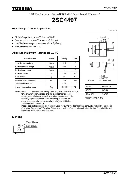
TOSHIBA Transistor Silicon NPN Triple Diffused Type (PCT process)2SC4497High Voltage Control Applications• High voltage: V CBO = 300 V, V CEO = 300 V • Low saturation voltage: V CE (sat) = 0.5 V (max) • Small collector output capacitance: C ob = 3 pF (typ.) • Complementary to 2SA1721Absolute Maximum Ratings (Ta = 25°C)Characteristics Symbol RatingUnitCollector-base voltage V CBO 300 V Collector-emitter voltage V CEO 300 V Emitter-base voltage V EBO 6 V Collector current I C 100 mA Base currentI B 20 mA Collector power dissipation P C 200 mW Junction temperature T j 150 °C Storage temperature rangeT stg−55~150 °CNote: Using continuously under heavy loads (e.g. the application of hightemperature/current/voltage and the significant change in temperature, etc.) may cause this product to decrease in thereliability significantly even if the operating conditions (i.e.operating temperature/current/voltage, etc.) are within the absolute maximum ratings.Please design the appropriate reliability upon reviewing the Toshiba Semiconductor Reliability Handbook (“Handling Precautions”/“Derating Concept and Methods”) and individual reliability data (i.e. reliability test report and estimated failure rate, etc).MarkingUnit: mmJEDEC TO-236MODJEITA SC-59TOSHIBA 2-3F1A Weight: 0.012 g (typ.)Electrical Characteristics (Ta = 25°C)Characteristics Symbol TestCondition MinTyp.Max Unit Collector cut-off current I CBO V CB= 300 V, I E= 0 ⎯ ⎯ 0.1 μA Emitter cut-off current I EBO V EB= 6 V, I C= 0 ⎯⎯ 0.1 μA Collector-base breakdown voltage V (BR) CBO I C= 0.1 mA, I E= 0 300 ⎯⎯ V Collector-emitter breakdown voltage V (BR) CEO I C= 1 mA, I B= 0 300 ⎯⎯ Vh FE (1)(Note)V CE= 10 V, I C= 20 mA 30 ⎯ 150DC current gainh FE (2)V CE= 10 V, I C= 1 mA 20 ⎯⎯Collector-emitter saturation voltage V CE (sat)I C= 20 mA, I B= 2 mA ⎯⎯ 0.5 V Base-emitter saturation voltage V BE (sat)I C= 20 mA, I B= 2 mA ⎯⎯ 1.2 V Transition frequency f T V CE= 10 V, I C= 10 mA ⎯ 70 ⎯ MHz Collector output capacitance C ob V CB= 20 V, I E= 0, f = 1 MHz ⎯ 3 4 pF Note: h FE (1) classification R: 30~90, O: 50~150RESTRICTIONS ON PRODUCT USE20070701-EN GENERAL •The information contained herein is subject to change without notice.•TOSHIBA is continually working to improve the quality and reliability of its products. Nevertheless, semiconductor devices in general can malfunction or fail due to their inherent electrical sensitivity and vulnerability to physical stress. It is the responsibility of the buyer, when utilizing TOSHIBA products, to comply with the standards of safety in making a safe design for the entire system, and to avoid situations in which a malfunction or failure of such TOSHIBA products could cause loss of human life, bodily injury or damage to property.In developing your designs, please ensure that TOSHIBA products are used within specified operating ranges as set forth in the most recent TOSHIBA products specifications. Also, please keep in mind the precautions and conditions set forth in the “Handling Guide for Semiconductor Devices,” or “TOSHIBA Semiconductor Reliability Handbook” etc.• The TOSHIBA products listed in this document are intended for usage in general electronics applications (computer, personal equipment, office equipment, measuring equipment, industrial robotics, domestic appliances, etc.).These TOSHIBA products are neither intended nor warranted for usage in equipment that requires extraordinarily high quality and/or reliability or a malfunction or failure of which may cause loss of human life or bodily injury (“Unintended Usage”). Unintended Usage include atomic energy control instruments, airplane or spaceship instruments, transportation instruments, traffic signal instruments, combustion control instruments, medical instruments, all types of safety devices, etc.. Unintended Usage of TOSHIBA products listed in his document shall be made at the customer’s own risk.•The products described in this document shall not be used or embedded to any downstream products of which manufacture, use and/or sale are prohibited under any applicable laws and regulations.• The information contained herein is presented only as a guide for the applications of our products. No responsibility is assumed by TOSHIBA for any infringements of patents or other rights of the third parties which may result from its use. No license is granted by implication or otherwise under any patents or other rights of TOSHIBA or the third parties.• Please contact your sales representative for product-by-product details in this document regarding RoHS compatibility. Please use these products in this document in compliance with all applicable laws and regulations that regulate the inclusion or use of controlled substances. Toshiba assumes no liability for damage or losses occurring as a result of noncompliance with applicable laws and regulations.。