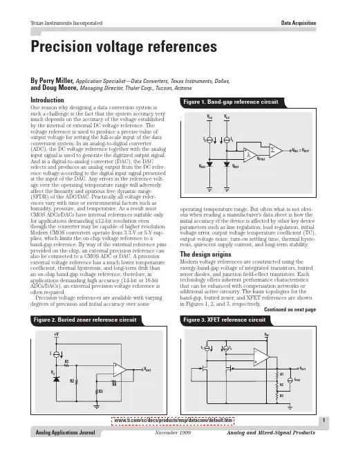
Precision voltage referencesIntroductionOne reason why designing a data conversion system is such a challenge is the fact that the system accuracy very much depends on the accuracy of the voltage established by the internal or external DC voltage reference. The voltage reference is used to produce a precise value of output voltage for setting the full-scale input of the data conversion system. In an analog-to-digital converter(ADC), the DC voltage reference together with the analog input signal is used to generate the digitized output signal.And in a digital-to-analog converter (DAC), the DACselects and produces an analog output from the DC refer-ence voltage according to the digital input signal presented at the input of the DAC. Any errors in the reference volt-age over the operating temperature range will adversely affect the linearity and spurious free dynamic range (SFDR) of the ADC/DAC. Practically all voltage refer-ences vary with time or environmental factors such as humidity, pressure, and temperature. As a result most CMOS ADCs/DACs have internal references suitable only for applications demanding ≤12-bit resolution eventhough the converter may be capable of higher resolution.Modern CMOS converters operate from 3.3-V or 5-V sup-plies, which limits the on-chip voltage reference to aband-gap reference. By way of the external reference pins provided on the chip, an external precision reference can also be connected to a CMOS ADC or DAC. A precision external voltage reference has a much lower temperature coefficient, thermal hysteresis, and long-term drift than an on-chip band-gap voltage reference; therefore, in applications demanding high accuracy (14-bit or 16-bit ADCs/DACs), an external precision voltage reference is often required.Precision voltage references are available with varying degrees of precision and initial accuracy over someoperating temperature range. But often what is not obvi-ous when reading a manufacturer’s data sheet is how theinitial accuracy of the device is affected by other key device parameters such as line regulation, load regulation, initial voltage error, output voltage temperature coefficient (TC),output voltage noise, turn-on settling time, thermal hyste-resis, quiescent supply current, and long-term stability.The design originsModern voltage references are constructed using the energy-band-gap voltage of integrated transistors, buried zener diodes, and junction field-effect transistors. Each technology offers inherent performance characteristics that can be enhanced with compensation networks or additional active circuitry. The basis topologies for the band-gap, buried zener, and XFET references are shown in Figures 1, 2, and 3, respectively.Texas Instruments Incorporated Data AcquisitionBy Perry Miller, Application Specialist—Data Converters, Texas Instruments, Dallas,and Doug Moore, Managing Director, Thaler Corp., Tucson, Arizona Continued on next pageTexas Instruments IncorporatedData AcquisitionBand-gap referenceAt its simplest, a band-gap reference is simply two tran-sistors with different emitter areas used for generating a voltage proportional to absolute temperature. V BE1and V BE2have opposite temperature coefficients. The voltage V CC is converted to a current I 1and I 2that are mirrored to the output branch. The output equation is(1)where λis the scale factor, V BE1is the base-emitter volt-age of the larger of the two transistors, and V BE2is thebase-emitter voltage of the second transistor.The band-gap references are widely used in ADC/DAC converters as well as for external reference source because they are fairly inexpensive. Generally, they are used in system designs where a maximum accuracy of 10 bits is required. Band-gap references typically have an initial error of 0.5–1.0% and a TC of 25–50 ppm/°C. The output voltage noise is typically 15–30 µV p-p (0.1–10 Hz) with a long-term stability of 20–30 ppm/1000 hrs.Zener referenceThe zener voltage reference and feedback amplifier shown in Figure 2 are used to provide a very stable output. A current source is used to bias a 6.3-V zener diode. The zener voltage is divided by the resistor network R1 and R2.This voltage is applied to the non-inverting input of the operational amplifier, which amplifies the voltage to the required output voltage. The amplifier gain is determined by the resistor networks R3 and R4, where G = 1 + R4/R3.A 6.3-V zener diode is used because it is the most stable zener diode over time and temperature.The output equation is(2)Buried zener diode references are more expensive than band-gap references but provide a higher performance level. They typically have an initial error of 0.01–0.04%, a TC of 1–10 ppm/°C, and less than 10-µV p-p (0.1- to 10-Hz)),V V (V V BE2BE1BE1O −λ+=noise. The long-term stability is typically 6–15 ppm/1000hrs. Buried zener-based references are frequently used for 12-bit, 14-bit, and higher resolution systems because the performance of the buried zener-based references can be extended by incorporating nonlinear temperature com-pensation networks into the design. The compensation network is trimmed at several temperatures to optimize the electrical performance over the operating tempera-ture range.XFET referenceThe XFET reference is a new reference technique that consists of two junction field-effect transistors, one of which has an extra channel implant to raise the pinch-off voltage. The two JFETs are run at the same drain current.The difference in pinch-off voltage is amplified and used to form a voltage reference. The general equation is(3)where ∆V P is the difference in pinch-off voltage betweenthe two FETs and I PTAT is the positive temperature coefficient correction current.The simplified schematic for the XFET reference is shown in Figure 3.The XFET references are relatively new and provide a performance level between band-gap and zener refer-ences.The initial error is typically 0.06%, a TC of 10 ppm/°C,and 15-µV p-p (0.1- to 10-Hz) noise. The long-term stability is 0.2 ppm/1000 hrs.Reference selection for a 14-bit converterSpecified parameters for voltage references include line regulation, load regulation, initial voltage error, output voltage temperature coefficient (TC), output voltage noise, turn-on settling time, thermal hysterisis, quiescent supply current, and long term stability.The most important parameters for data acquisition systems design are initial error, output voltage tempera-ture coefficient (TC), thermal hysteresis, noise, and long-term stability of the voltage reference device.Table 1 summarizes the major error sources for the three references that are compared in this application note. The data represents the highest grade for each)(R3),(I R1R3R2R1V V PTAT P O +++∆=Table 1. Voltage reference major error sources (all information is based on published data sheets)Continued from previous page× V . ZR3R41R2R1R2V O++=Texas Instruments Incorporated Data Acquisitionrespective model in the 8-pin plastic DIP package over the industrial temperature range (–40°C to +85°C). The poorest-performing references are band-gap type and are not included in this summary. Buried zener diodes have better overall performance than band-gap devices and the XFET references. The buried zener reference with a third-order temperature compensation network (VRE3050) is the best performer with respect to initial error, TC, and thermal hysteresis.Explanation of parametersInitial error—The output voltage tolerance of a refer-ence after the device is turned on and warmed up. It is usually measured without a load applied. In many applica-tions, initial error is the most important specification.Often instrument manufacturers will specify a reference with a tight initial error so they do not have to perform room-temperature systems calibration after assembly.Temperature coefficient (TC)—A change in output voltage due to change in temperature usually expressed in ppm/°C. It is the second most important specification after initial accuracy. For many instrument manufacturers,a voltage reference with a temperature coefficient less than 1 ppm/°C makes it possible not to have to perform a system temperature calibration, a slow and costly process.Of the three TC specification methods (slope, butterfly,and box), the box method is most commonly used. A box is formed by the min/max limits for the nominal output voltage over the operating temperature range. The equa-tion follows.(4)6MIN MAX nominal MIN MAX 10)T (T V V V TC ×−×−=This method corresponds more accurately to the method of test and provides a closer estimate of actual error than the other methods. The box method guarantees limits for the temperature error but does not specify the exact shape and slope of the device under test. Assuming a 5-V reference with a 0.6-ppm/°C TC over the industrial tem-perature range, a plot of the box calculation method would appear as in Figure 4.A designer who needs a 14-bit accurate data acquisition system over the industrial temperature range (–40°C to +85°C) will need a voltage reference with a TC of 1.0 ppm/°C if the reference is allowed to contribute an error equivalent to 1 LSB. For 1/2 LSB equivalent error from the reference, a voltage reference with a tempera-ture coefficient of 0.5 ppm/°C would be needed. Figure 5shows the required reference TC vs. ∆T change from25°C for resolution rang-ing from 8 bits to 20 bits.Thermal hysteresis—A change in output voltage as a result of a tempera-ture change. When references experience a temperature change and return to the initial tem-perature, they do not always have the same initial output voltage.Thermal hysteresis is dif-ficult to correct and is a major error source in sys-tems that experience tem-perature changes of 25°C or more. Voltage refer-ence manufacturers are starting to include this important specification in their datasheets.Continued on next pageTexas Instruments IncorporatedData AcquisitionNoise (1/f and broadband)—Electrical noise on the output of a voltage reference. It can include wideband ther-mal noise and narrowband 1/f noise.Wideband noise can be effectively filtered with a simple RC network. 1/f noise is inherent in the reference and cannot be filtered. It is specified in the 0.1- to 10-Hz range. Low 1/f noise refer-ences are important in precision designs.Long-term drift—A slow change inoutput voltage that occurs over months of operation. Long-term drift is usually expressed in ppm/1000 hrs. In zener references, the long-term drift is typi-cally 6 ppm/1000 hrs. and decreases atan exponential rate over time. Additional temperature burn-in of the reference can accelerate the stability of a zener reference. The XFET reference has excellent long-term stability—0.2 ppm/1000 hrs.Turn-on settling time—A change in voltage over a specified time interval after the power is applied. Most references settle to 0.1% in less than 10 µs. Turn-on settling time is important for portable battery systems that conserve energy by powering the circuitry only for short periods of time.Line regulation—An error produced by a change in the input voltage. This dc specification does not include the effects of ripple voltage or line transients.Load regulation—An error produced by a change in load current. Like line regulation, this dc specification does not include the effects of load transients.PCB layout—Poor printed circuit board layout can adversely affect the performance of the reference. Poor layout can affect the output voltage, noise, and thermal performance of the device. Inherent stress in the PCB can also be transferred to the reference and can shift the out-put voltage.ConclusionIt has been shown that a number of key parameters must be evaluated before selecting an external reference for a high-resolution data acquisition system. The XFET refer-ence is suitable for systems that will be held at a constant temperature and where good long-term stability of the reference is important. In 14-bit conversion systems that are designed for the industrial operating temperature range, the VRE3050 is the preferred device because of its better initial error, TC, and thermal hysteresis performance.References1.Analog Devices Inc., Low Noise, Micropower,Precision Reference ADR293 Datasheet.2.Paul R. Gray and Robert G. Meyer, Analysis and Design of Analog Integrated Circuits ,3rd ed. (John Wiley & Sons, Inc., 1992).3.Maxim Corp., MAX6250, Low Noise Precision,+2.5 V +4.096 V +5 V Voltage Reference Datasheet.4.Texas Instruments, THS1265, 12-bit, 65 MSPS,IF Sampling Communications A/D converter.5.Texas Instruments, THS1470, 14-bit, 70 MSPS,IF Sampling Communications A/D converter.6.Thaler Corp., Precision Reference VRE3050Datasheet.Continued from previous pageIMPORTANT NOTICETexas Instruments Incorporated and its subsidiaries (TI) reserve the right to make corrections, modifications, enhancements, improvements, and other changes to its products and services at any time and to discontinue any product or service without notice. Customers should obtain the latest relevant information before placing orders and should verify that such information is current and complete. All products are sold subject to TI's terms and conditions of sale supplied at the time of order acknowledgment. TI warrants performance of its hardware products to the specifications applicable at the time of sale in accordance with TI's standard warranty. Testing and other quality control techniques are used to the extent TI deems necessary to support this warranty. Except where mandated by government requirements, testing of all parameters of each product is not necessarily performed.TI assumes no liability for applications assistance or customer product design. Customers are responsible for their products and applications using TI components. To minimize the risks associated with customer products and applications, customers should provide adequate design and operating safeguards.TI does not warrant or represent that any license, either express or implied, is granted under any TI patent right, copyright, mask work right, or other TI intellectual property right relating to any combination, machine, or process in which TI products or services are used. Information published by TI regarding third-party products or services does not constitute a license from TI to use such products or services or a warranty or endorsement thereof. Use of such information may require a license from a third party under the patents or other intellectual property of the third party, or a license from TI under the patents or other intellectual property of TI. Reproduction of information in TI data books or data sheets is permissible only if reproduction is without alteration and is accompanied by all associated warranties, conditions, limitations, and notices. Reproduction of this information with alteration is an unfair and deceptive business practice. TI is not responsible or liable for such altered documentation.Resale of TI products or services with statements different from or beyond the parameters stated by TI for that product or service voids all express and any implied warranties for the associated TI product or service and is an unfair and deceptive business practice. TI is not responsible or liable for any such statements. Following are URLs where you can obtain information on other Texas Instruments products and application solutions: TI Worldwide Technical Support InternetTI Semiconductor Product Information Center Home PageTI Semiconductor KnowledgeBase Home Page/sc/knowledgebaseProduct Information CentersAmericasPhone+1(972) 644-5580Fax+1(972) 927-6377 Internet/Email /sc/pic/americas.htmEurope, Middle East, and AfricaPhoneBelgium (English)+32 (0) 27 45 54 32Netherlands (English)+31 (0) 546 87 95 45 Finland (English)+358 (0) 9 25173948Russia+7 (0) 95 7850415 France+33 (0) 1 30 70 11 64Spain+34 902 35 40 28 Germany+49 (0) 8161 80 33 11Sweden (English)+46 (0) 8587 555 22 Israel (English)1800 949 0107United Kingdom+44 (0) 1604 66 33 99 Italy800 79 11 37Fax+(49) (0) 8161 80 2045Internet /sc/pic/euro.htmJapanFaxInternational+81-3-3344-5317Domestic0120-81-0036 Internet/EmailInternational /sc/pic/japan.htmDomestic www.tij.co.jp/picAsiaPhoneInternational+886-2-23786800Domestic Toll-Free Number Toll-Free Number Australia1-800-999-084New Zealand0800-446-934China800-820-8682Philippines1-800-765-7404 Hong Kong800-96-5941Singapore800-886-1028Indonesia001-803-8861-1006Taiwan0800-006800Korea080-551-2804Thailand001-800-886-0010 Malaysia1-800-80-3973Fax886-2-2378-6808Email tiasia@ Internet /sc/pic/asia.htm ti-china@C011905 Safe Harbor Statement:This publication may contain forward-looking statements that involve a number of risks and uncertainties. These “forward-looking statements” are intended to qualify for the safe harbor from liability established by the Private Securities Litigation Reform Act of 1995. These forward-looking statements generally can be identified by phrases such as TI or its management “believes,” “expects,” “anticipates,”“foresees,” “forecasts,” “estimates” or other words or phrases of similar import. Similarly, such statements herein that describe the company's products, business strategy, outlook, objectives, plans, intentions or goals also are forward-looking statements. All such forward-looking statements are subject to certain risks and uncertainties that could cause actual results to differ materially from those in forward-looking statements. Please refer to TI's most recent Form 10-K for more information on the risks and uncertainties that could materially affect future results of operations. We disclaim any intention or obligation to update any forward-looking statements as a result of developments occurring after the date of this publication.Trademarks: All trademarks are the property of theirrespective owners.Mailing Address: Texas InstrumentsPost Office Box 655303Dallas, Texas 75265© 2005 Texas Instruments IncorporatedSLYT183。