DAC904E中文资料
- 格式:pdf
- 大小:551.18 KB
- 文档页数:21

使用说明书EXTRAmatic 9040安全常伴您左右KaVo Dental GmbH Wangener Straße 78D-88299 Leutkirch++ 49 (0) 7561 86-0++ 49 (0) 7561/86-400目录1用户说明1.1用户指南1.1.1 标志1.1.2 目标对象1.1.3 缩略语1.2 服务1.3 保修条件1.4 运输和储存1.4.1 德国1998年8月28包装条例1.4.2 运输损坏1.4.3 储存2安全2.1 安全使用说明2.1.1 危险级别说明2.1.2 结构2.2 预定用途2.2.1 概述2.2.2 产品具体信息2.3 安全说明2.3.1 概述2.4 防护衣3 产品描述3.1 EXTRAmatic 前面3.2 EXTRAmatic 后面3.3 控制面板3.4 技术参数3.5铭牌4 启动4.1 试运行的准备4.1.1 搬运产品4.2 连接组件4.2.1在工作场所的连接4.2.2在牙科技工中心的连接4.2.3连接吸尘软管4.2.4 水平校准4.2.5 连接控制线4.2.6 连接导线4.2.7 连接脚踏开关4.2.8 连接外控面板4.2.9 连接电源5. 操作5.1 各程序的功用5.2用户程序5.2.1 水平面测量5.2.2 自动模式5.2.3 连续模式5.2.4预设吸尘强度等级5.3 应用程序5.3.1 应用程序按键(2000)5.3.2 “用户系统”应用程序(2050)5.3.3 “用户设定检查”应用程序(2100)5.3.4 “数字语言”应用程序(2150)5.3.5 “标准屏幕”应用程序(2800)5.3.6 “初始化存储器”应用程序(2250)5.3.7 “自动感应调节”应用程序(2300)5.3.8 “手动感应调节”应用程序(2350)5.3.9 “接口气压显示“应用程序(2400)5.3.10 “活性碳过滤器控制”应用程序(2500)5.3.11 “修改活性碳过滤器使用时间”应用程序(2450)5.3.12 “活性碳过滤器更换后所经过的时间”应用程序(2455)5.3.13 “重新设定活性碳过滤器监测时间”应用程序(2550)5.3.14 “延续工作时间”应用程序(2600)5.3.15 “记忆时间”应用程序(2650)5.3.16 “SW 版本”应用程序(2700)5.3.17 “过滤器清洁间隔时间”应用程序(2750)6 保养方法6.1 清洁6.2 维护6.2.1 更换垃圾袋6.2.2 更换活性碳过滤器6.2.3 更换长期过滤器6.2.4 警示灯7 故障检修8 附件1 用户说明1.1 用户指南要求请于首次使用本产品前,认真阅读以下说明,以避免错误操作及产品损坏。
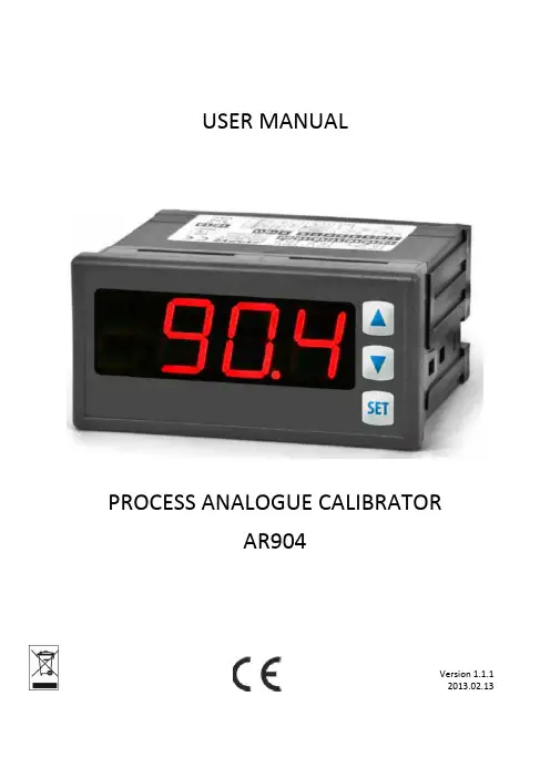
USER MANUALPROCESS ANALOGUE CALIBRATORAR904Version 1.1.12013.02.13Thank you for choosing our product.This user manual will help you with proper and safeoperation and full use of the process analogue calibrator device.Before installing and operating, please readand understand this manual.If you have any additional questions, please contact the technical advisor. TABLE OF CONTENTSPay special attention to information marked with this sign!Manufacturer reserves the right to make changes in design and software of the device without compromising technical parameters1.SAFETY PRECAUTIONS▪Before using the unit, please read this manual carefully.▪To avoid electrical shock or damage to the device, mechanical and electrical installation have to be performed by a qualified personnel.▪Before turning on the power make sure that all cables are properly connected.▪Before making any modifications to the wiring connections, turn off all voltages applied to the device. ▪You have to ensure proper working conditions, according to the specifications of the device (power supply voltage, humidity, temperature, chapter 5).2.INSTALLATION NOTESThis instrument was designed to provide the appropriate level of resistance to most disturbances that may occur in industrial environments. In environments with unknown level of interference it is recommended to use the following measures to prevent possible interference with operation of the instrument:▪Do not power supply the device from the same line as the power component without the appropriate network filters.▪Use only shielded power and signal cables taking into account that the grounding of the shield should bea single point, made as close to the device as possible.▪Avoid placing signal cables very close and parallel to energy and power cables.▪It is recommended to twist signal cables in pairs.▪Avoid proximity of remote controlled devices, electromagnetic meters, high power loads, loads with phase or group power control and other devices that generate large impulse disturbances.▪Ground or zero metal rails that are used to mount rail devices.Before using the device, remove the protective film from the LED display.3.GENERAL PROCESS ANALOGUE CALIBRATOR CHARACTERISTICS▪This device allows you to control or test devices with current or voltage input (proportional valves, servomotors, inverters, motors, etc.)▪ 2 analogue outputs (working simultaneously):-current 4÷20mA or 0÷20mA (active, cannot be powered from 2 wires current loop)-voltage 0÷10V▪Soft start/stop (ramping) or triangle wave generator with manual or automatic (activated after device power on) trigger.▪Programmable setpoint value, output signal change step, display range, soft start/stop options, communication options, access options and other configuration parameters.▪7-segment LED display with brightness adjustment.▪Optional RS485/RS232 serial interface (galvanically isolated, MODBUS-RTU protocol).▪Parameters configuration methods:-Using IP65 foil keyboard located on the device front panel-Using AR955 programmer or RS485/RS232 interface with PC software (Windows 2000/XP/Vista/7)▪Available free software that allows parameters configuration.▪Access to configuration parameters can be password protected.▪High accuracy and high resistance to interference.▪Available accessories:-AR955 programmer-RS485 to USB converterCAUTION:Before starting work with the process analogue calibrator, read this manual carefully and perform electrical and mechanical installation properly and set parameters correctly.4.PACKAGE CONTENTS▪Process analogue calibrator▪User manual▪Warranty card5.TECHNICAL DATA(1)- Output cannot be powered from two wires current loop6.HOUSING DIMMENSIONS AND INSTALLATION DATA7.TERMINAL STRIPS AND ELECTRICAL CONNECTIONS DESCRIPTIONa)Terminals and output signals descriptionOnly AR955 programmer can be connected to PRG socket. Connecting other devices to PRG socket can damage connected device and AR904 process analogue calibrator.8.BUTTONS DESCRIPTIONa) Buttons functions in setpoint value display mode (normal mode)) )and 9: b) Buttons functions in parameters configuration mode (chapter 10)9.OUTPUTS SETPOINT VALUE CHANGEPressing [UP] or [DOWN] button while setpoint value is being displayed will change the value by pre-set step(parameter 6: , chapter 10, table 10). Changes of the output signal are proportional to changes of the displayed value. Pressing [SET] + [DOWN] buttons together will set output value immediately to lower rangevalue (2: or 4: ) while pressing [SET] + [UP] buttons together will set output value immediately to upperrange value (3: or 5: ). In addition, the output signal may be given also in parameters programming mode(parameter 7: ) and using serial interface RS485/RS232 or AR955 programmer (chapter 15, table 15). Moreover, it is possible to set the setpoint value outside of the display range based on the parameters 2: and 3:. The value of this override that can be set using the buttons is ±5% for 4÷20mA (2÷10V) output and 6,2% for the remaining outputs.10.CONFIGURATION PARAMETERS SETUPAll configuration parameters of the device are saved in the non-volatile EEPROM internal memory. Two parameters configuration methods are available:ing IP65 foil keyboard located on the front panel of the device:-From the setpoint value display mode enter configuration menu (press and hold for more than 1 second [UP] and [DOWN] buttons together). If parameter 13: (password protection is turned on), display will show message and then with first digit blinking. Using [UP] or [DOWN] button enter protection password (by default parameter 12: ). To proceed to the next digit or confirm the code use [SET] button.-After opening configuration menu you will see mnemonic parameter names ( <-> <-> <-> etc.), [UP] button will proceed to the next parameter and [DOWN] button will go back to theprevious parameter (all parameters are listed in table 10).-To change or display current parameter value press the [SET] button.-Using [UP] or [DOWN] button change the edited parameter value.-Confirm modified value using [SET] button or cancel using [UP] and [DOWN] buttons (simultaneously), then parameter name will be displayed.ing RS485/RS232 port or AR955 programmer and pc software ARSOFT-WZ1:-Connect process analogue calibrator to the PC port and start ARSOFT-WZ1 application.-After connection is established application window will display current setpoint value.-Device parameters can be displayed and modified in the parameters configuration window.-New paramete rs values have to be saved using “Zatwierdź zmiany” button.-Current configuration can be saved in a file or can be read from the file.CAUTION:-Do not use RS485/RS232 port and AR955 programmer simultaneously, because communication errors will occur.Table 10. Configuration parameters0: currentdot position(0.0)display units – display for 0mA, 4mA, 0V – lower output rangedisplay units – display for 20mA, 10V – upper output rangesetpoint units – lower setpoint value limit (parameter 7: )when set using buttonssetpoint units – upper setpoint value limit (parameter 7: )when set using buttonsvalue units, setpoint value change step (parameter 7: ) when setusing buttonssetpoint or 4:or 5: , changes step: 6:soft start The duration of the rising edge (ramp). Function isturned on for value (description in chapter 11) soft stop The duration of the falling edge (ramp). Function isturned on for value (description in chapter 11) rampsetpointdisplay (10% step)RS485/RS232 kbit/s kbit/s kbit/s kbit/s kbit/s kbit/s11.SOFT START/STOP AND TRIANGLE WAVEFORM GENERATORThis device has soft start and stop (ramp) function. This function works as shown on the below charts (illustrations 11.1, 11.2, 11,3). To turn on this function you will have to configure soft start time (rising slope,parameter 8: , chapter 10) or soft stop time (falling slope, parameter 9: ) and trigger mode (parameter10: ). If both times are different than 0 (8: and 9: ) device outputs will generate triangle periodicalsignal. Amplitudes (end values) of output signals are defined by parameter 2: , 3: , 4: and 5:. Function is activated automatically after device power on (when parameter 10: ) or manually (10: ) using [SET] button (pressed and hold for more than 1.5 seconds). Moreover ramp function can be stopped and resumed at any time using [SET] button (short message will be displayed - start or - stop). Output status in this mode is refreshed 4 times per second.Illustration 11.1. Output status in soft start mode (parameter ).Illustration 11.2. Output status in soft stop mode (parameter ).Illustration 11.3. Output status in triangle signal generator mode (parameter ).12.MESSAGES AND ERRORS LISTFollowing short messages can be displayed during device operation:13.RS485 COMMUNICATION INTERFACE (per EIA RS-485)Maximum RS485 cable length – 1km.Maximum number of devices in RS485 line – 30. To increase this number you can use RS485/RS485 repeater. Terminal resistors when MASTER is on the line beginning (above illustration):-On the line beginning –2 x 820Ω to ground and +5V of the MASTER and 150Ω between lines,- On the line end - 150Ω between lines.Terminal resistors when MASTER is in the middle of the line:- Near the converter – 2 x 820Ω to ground and +5V of the converter, - On both line ends – each end 150Ω between lines.14. RS232C COMMUNICATION INTERFACE (per EIA RS-232C)15. MODBUS-RTU SERIAL TRANSMISSION PROTOCOL Character format:8 bits, 1 stop bit, no parity bitAvailable functions: READ – 3 or 4, WRITE – 6Table 15.1. Request frame format for READ function (frame length – 8 Bytes):Table 15.2. Request frame format for WRITE function (frame length– 8 Bytes):Table 15.3. Response frame format for READ function (minimum frame length – 7 Bytes):Table 15.4. Response frame format for WRITE function (frame length – 8 Bytes):Table 15.5. Special response (errors: function field = 0x84 or 0x83 for READ function and 0x86 for WRITE function):Table 15.6. MODBUS-RTU protocol registers mapParameter 0:Parameter 1: dot positionParameter 2: display lower rangeParameter 3:Parameter 4:Parameter 5:Parameter 6:Parameter 7:Parameter 8:Parameter 9:Parameter 10:Parameter 11:Parameter 12:Parameter 13:Parameter 14:Parameter 15:Parameter 16:ER NOTES。

Notice d‘emploiContenu Contenu• e 604• pince de fixation MZH 604• étui• guide de démarrage rapide• consignes de sécuritéVue d’ensemble du produit1. Grille de protection2. Connecteur XLR-33. Pince de fixationInstallationFixer le microphoneVissez le support au microphone à l’aide de la vis.Raccorder le microphoneRaccordez la prise XLR-3 du câble de microphone (accessories optionnels) à la prise XLR-3 du microphone.UtilisationPlacement du microphone sur la caisseUtilisez la pince pour fixer le e 904 au bord de la caisse.Positionnez le microphone sur le tambour avec un écart entre 3 et 5 cm au-dessus de sa surface.3 – 5 cm (1.2 – 2")Il est indispensable d’observer les indications suivantes :Pos.Type de son obtenu CommentaireABeaucoup de son fonda-mentalPeu de sons harmoniques Positionnement sur la caisse 3 à 5 cm au-dessus de la peauLe rapport son fondamental/harmoniques peut être réglé par l’angle.Un angle de 30 à 60° fournit les résultats les plus harmonieux.BPeu de son fondamental Beaucoup de sons harmo-niquesCEmploi d’un deuxième microphone e 604 pour la prise de son sur la peau de résonance et les caisses claires.Le micro du bas doit être configuré en inversion de phase pour éviter des problèmes d’annulation dephase.A CBNettoyage et entretien du e 604Placement des enceintes de retourPour éviter tout Larsen et une faible isolation par rapport aux autres sources sonores, placez les enceintes de retour de façon à ce qu’elles se trouvent dans l’angle d’atténuation maximale du microphone (env. 180°).Nettoyage et entretien du e 604ATTENTIONLES LIQUIDES PEUVENT ENDOMMAGER LES COMPOSANTS ÉLECTRONIQUES DU PRODUIT !Une infiltration de liquide dans le boîtier du produit peut causer des courts-circuits et endommager les composants électroniques.Éloignez tout type de liquide du produit.N’utilisez jamais de solvant ou de détergent.Débranchez les produits du secteur et enlevez les packs accus et packs piles avant le nettoyage.Ne nettoyez les produits qu’avec un chiffon doux et sec.Caractéristiques techniquesCaractéristiques techniquesTransducteurdynamique Réponse en fréquence 40 - 18 000 H z Directivitécardioïde Sensibilité (champ libre, à vide)2,0 mV/Pa Impédance nominale (à 1 kHz)350 ΩImpédance de charge mini. 1 k ΩConnecteur XLR-3Dimensions Ø 41 m m, longueur 63 m m Poids125 gDiagramme polaire125 Hz 250 Hz 500 Hz 1,000 Hz 2,000 Hz 4,000 Hz8,000 Hz 16,000 Hz30°0°180°150°120°60°90°0510152025dB30°0°180°150°120°60°90°Réponse en fréquence-40-50-60-70-80-90501002005001,0002,0005,00010,00020,000H zdBV 0°, 1 mVue d’ensemble des applicationsBrochage du connecteurUNBALANCEDBALANCEDVue d’ensemble des applicationsApplication principale Application annexe。

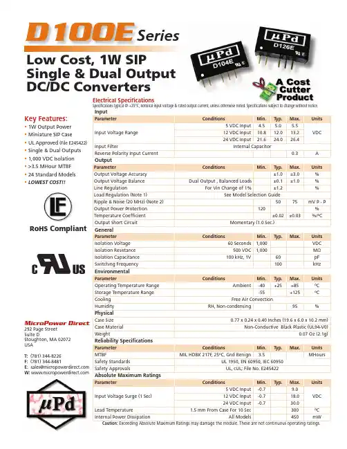
MicroPower Direct292 Page Street Suite DStoughton, MA 02072USAT: (781) 344-8226F: (781) 344-8481E: sales@ W: Key Features:• 1W Output Power • Miniature SIP Case • UL Approved (File E245422)• Single & Dual Outputs • 1,000 VDC Isolation • >3.5 MHour MTBF • 24 Standard Models •LOWEST COST!!D100E Low Cost, 1W SIPSingle & Dual Output DC/DC Con v ert e rsSeriesRoHS CompliantDerating CurveMechanical DimensionsNotes:1. Output load regulation is specifi ed for a load change of 10% to 100%.2. T hese units should not be operated with a load under 10% of full load.Operation at no-load may cause damage to the unit.3. These converters will operate without external components. However,when measuring output ripple, it is recommended that an externalto common for dualoutput units. An in-put capacitor will enhance stability over temperature and input linevariations. Recommended capacitor values are given in the table above.For applications requiring very low output noise levels, a simple LC fi ltershould be effective.4. D ual output units may be connected to provide a 10V, 18V, 24V or 30VDC output. To do this, connect the load across the positive (+Vout) andnegative (-Vout) outputs and fl oat the output common5. It is recommended that a fuse be used on the input of a power supply forprotection. See the Model Selection table above for the correct rating.Other input/output combinations are available(i.e. 3.3 VDC). Contact the factory for details at:sales@MicroPower Direct292 Page Street Ste D Stoughton, MA 02072 • TEL: (781) 344-8226 • FAX: (781) 344-8481 • E-Mail: sales@。
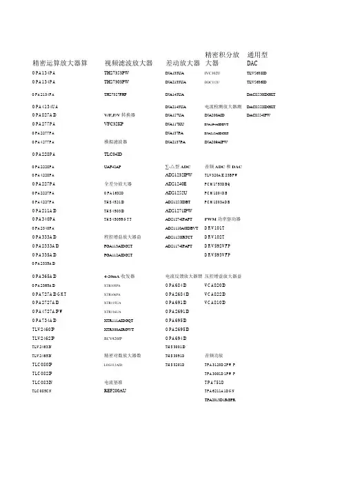
Part Number价格(美元)ADS1115IDGST 2.55 ADS1130IPW 2.55 ADS1146IPW 3.25 ADS1148IPW 4.75 ADS1174IPAPT 6.9 ADS1246IPW 4.15 ADS1248IPW 5.95 ADS1271IPW7.6 ADS1274IPAPT15.45 ADS7818P 2.5 ADS7863IDBQ 5.8 ADS7882IPFBT 2.9 ADS7883SBDBVT 2.5 ADS7950SDBT 2.8 ADS803E11.25 ADS805E11.9 ADS807E13.3 ADS828E12.9 ADS8317IDGKT 5.75 ADS8318IDGST8.05 ADS8319IDGST 6.9 ADS831E 4.75 ADS8326IDGKT 5.75 ADS8331IBPW7.3 ADS8361IDBQ10.5 ADS8504IBDW12.5 ADS8505IDW14.95 ADS8508IBDW11.95 ADS8509IDW11.95 BUF634P 3.5 BUF634U 4.2 CDCE62002RHBT7.6 CDCE925PW 2.35 CDCM61002RHBT 5.75 CDCM7005RGZT11 CSD17307Q5A0.406 CSD17312Q5 1.3 CSD25302Q20.207 DAC5662IPFB12.75 DAC5672IPFB15.7 DAC7611P 4.05 DAC7612U 3.75 DAC7811IDGS 3.1 DAC7821IPW 3.15 DAC7822IRTAT 4.4 DAC8552IDGKT 3.7 DAC8801IDGKT 5.3 DAC8802IPW7.35 DAC8805QDBT7.35 DAC8806IDB 6.6 DAC8811IBDGKT8.25 DAC8812IBPW10.1 DAC8820IBDB10.2 DAC8822QBDBT10.4 DAC902E8.1DAC904E10 DRV592VFP 2.25 DRV593VFP12.3 DRV8332DKD 5.65 DRV8801PWP 1.5 DRV8811PWP 2.2 DRV8812PWP 1.95 DRV8828PWP 1.95 INA118P 4.8 INA122PA 2.45 INA128PA 3.05 INA133UA 1.4 INA134PA 1.05 INA143UA 1.3 INA2133UA 1.8 INA2134PA 1.7 INA2143UA 1.7 INA271AID0.48 INA282AID 1.4 INA333AIDGKT 2.1 IVC102U 5.45 LM3S8962-IQC50-A2 6.45 LM3S9B92-IQC80-C57.95 LOG112AID9.5 LOG114AIRGVT 5.2 LP2951D0.333 MC33063AP0.252 MSP430F249TPM 4.35 MSP430F2618TPM 6.35 MSP430F449IPZ 5.15 MSP430F5438AIPZ 4.85 MSP430FG4618IPZ8.35 OPA134PA 1.1 OPA140AID 1.9 OPA1611AID 2.1 OPA1612AID 3.3 OPA1632D 2.1 OPA209AID 1.15 OPA2134PA 1.25 OPA2209AID2 OPA2227PA 1.85 OPA2228PA 1.85 OPA2234UA 2.25 OPA2251PA 1.95 OPA227PA 1.1 OPA228PA 1.1 OPA2330AID0.8 OPA234UA 1.25 OPA2365AID 1.15 OPA251PA 1.15 OPA2684ID 2.45 OPA2691ID 2.75 OPA2695ID 2.6 OPA2727AID 1.2 OPA2830ID0.95 OPA2889ID 1.45OPA2890ID 1.45 OPA300AID0.9 OPA330AID0.55 OPA355UA0.85 OPA365AID0.8 OPA453TA 2.55 OPA454AIDDA 3.3 OPA4872ID 2.6 OPA548FKTWT 6.9 OPA549T12 OPA561PWP 3.35 OPA564AIDWP 3.3 OPA567AIRHGT 2.65 OPA569AIDWP 4.7 OPA615ID 6.05 OPA656U 4.3 OPA684ID 1.6 OPA690ID 1.6 OPA691ID 1.75 OPA692ID 1.4 OPA692ID 1.4 OPA694ID 1.5 OPA695ID 1.6 OPA735AID 1.5 OPA820ID 1.1 OPA830ID0.6 OPA842ID 1.8 OPA843ID 1.85 OPA847ID 2.4 OPA860ID 2.9 OPA890ID0.9 PCM1753DBQ 1.25 PCM1803ADB 1.35 PCM1804DB 4.75 PGA112AIDGST 1.15 PGA113AIDGST 1.15 PGA202KP7.75 PGA203KP7.75 PGA280AIPW 3.5 RCV420JP 3.55 REF200AU 3.1 SN10501D0.85 SN10502D 1.45 SN65HVD1050D0.55 THS3001HVIDGN 6.6 THS3001ID 4.05 THS3091DDA 3.4 THS3092DDA 6.1 THS3201D 2.55 THS4012ID 3.65 THS4031ID 2.25 THS4032ID4 THS4032ID4 THS4151ID 6.1 THS4271D 2.7 THS4501ID 4.45THS4503ID 4.85 THS4521ID 1.35 THS4631D 4.3 TL1963ADCQT 1.35 TL2575HV-ADJIKV 1.15 TLC04ID 1.4 TLC372IP0.389 TLV3501AID 1.2 TLV5638ID6 TMP275AID 1.5 TMS320F2808PZA11.6 TMS320F2812PGFA15.75 TMS320F28335PGFA15.65 TPS28225D0.75 TPS2828DBVT0.7 TPS2829DBVT0.7 TPS40200D0.9 TPS40210DGQ 1.2 TPS40211DGQ 1.2 TPS54160DGQ 2.3 TPS5430DDA 2.25 TPS54331D 1.65 TPS5450DDA 2.7 TPS60400DBVT0.38 TPS61029DRCT 1.3 TPS61085PW 1.15 TPS61087DRCT 1.85 TPS61175PWP 2.2 TPS61200DRCT 1.3 TPS62040DGQ 1.7 TPS62110RSAT 1.55 TPS63000DRCT 1.75 TPS63700DRCT 1.9 TPS70302PWP 2.8 TPS74901KTWT2 TPS75901KTTT 3.7 TPS78001DDCT0.397 TPS78601KTTT 1.8 UAF42AP7.55 UC3846N 1.9 UC3854AN 1.65 UCC25600D0.85 UCC27200D 1.6 UCC27201D 1.6 UCC27321P 1.3 UCC27322P 1.3 UCC27323P0.95 UCC27324P0.95 UCC27325P0.95 UCC28019AP0.9 UCC28060D 1.45 UCC28220D 2.4 UCC28600D0.48 UCC3808N-1 1.2 UCC3808N-2 1.2 UCC384DP-ADJ 2.35UCC38C43P0.85 UCD7100PWP 1.2 UCD7201PWP 1.75 VCA810ID7.4 VCA820ID 3.4 VCA821ID 3.4 VCA822ID 3.4 VCA824ID 3.4 VFC32KP 4.8 XTR105PA 4.6 XTR106PA4 XTR111AIDGQT0.75 XTR115UA 1.5 XTR116UA 1.25 XTR300AIRGWT 2.2Simple Description具有集成 MUX、PGA、比较器、振荡器和参考的 16 位 ADC用于桥传感器的 18 位模数转换器用于温度传感器的 16 位模数转换器用于温度传感器的 16 位模数转换器四路 16 位同步采样模数转换器低噪音、精密 24 位模数转换器具有集成低噪声 PGA(增益为 128 时偏移仅为 48nV)的精密 24 位 ADC24 位 105kSPS 工业 Δ-Σ ADC四路、128kHz、24 位同步采样 Σ-Δ ADC12 位高速低功耗采样模数转换器双路、2MSPS、12 位、3+3 或 2+2 通道、同步采样模数 SAR 转换器具有 Ref 引脚的 2.7V-5.25V 数字、5V 模拟 12 位 3MSP 并行 ADC2.7V-5.5V 12 位 3MSPS 串行 ADC12 位、1MSPS、4 通道、单端、微功耗、串行接口、SAR ADC12 位 5MSPS ADC,具有内部/外部基准、2 至 5Vpp 之间的灵活 I/P、超出范围指示信号和引脚兼容12 位 20 MSPS ADC,具有内部/外部参考、2 至 5Vpp 之间的灵活 I/P、超出范围指示信号和引脚兼容12 位 53MSPS ADC,具有单端/差动输入、2 到 3Vpp 范围、内部/外部参考和超出范围指示10 位 75MSPS ADC,具有单端/差动输入、内部/外部参考、可可编程 i/p 范围和断电功能,并与 ADS822/3/5/6 兼容16 位、准双极、全差动输入、250kSPS 串行输出、2.7V 到 5.5V 微功耗采样 ADC16 位单极差动输入 500kSPS 串行输出的 4.5V 至 5.5V 微功耗采样 ADC采用 MSOP-10 封装的16 位精密 SAR8 位 80MSPS ADC,具有单端/差动输入、内部基准和可编程输入范围16 位伪差动输入 250kSPS 串行输出的 2.7V 至 5.5V 微功耗采样 ADC2.7V-5.5V 16 位 500KSPS 低功耗串行 ADC4 通道串行输出 16 位 500kSPS 2 ADC具有并行接口的 12 位 250kHz CMOS 模数转换器,2.5V 内部参考16 位 250kHz CMOS 模数转换器,具有串行接口和 2.5V 内部参考具有串行接口的 12 位 250kHz CMOS 模数转换器,2.5V 内部参考16 位 250kHz CMOS 模数转换器,具有串行接口和 2.5V 内部参考250mA 高速缓冲器250mA 高速缓冲器具有集成双路 VCO 的 4 路输出时钟发生器/抖动消除器具有 2.5V 或 3.3V LVCMOS 输出的可编程 2-PLL VCXO 时钟合成器1:2 超低抖动晶体时钟发生器高性能、低相位噪声、低偏移的时钟同步器(使参考时钟与 VCXO 同步)30V N 通道 NexFET™ 功率 MOSFET30V N 通道 NexFET™ 功率 MOSFETP 通道 NexFET™ 功率 MOSFET12 位 200MSPS 双 DAC数模转换器12 位串行输入数模转换器双路 12 位串行输入数模转换器12 位串行输入乘法数模转换器12 位串行输入乘法 DAC双路 12 位串行输入乘法 DACDAC8552:16 位双路电压输出数模转换器14 位单通道串行接口乘法数模转换器14 位双通道串行接口乘法数模转换器Dual, Parallel Input, 14-Bit, Multiplying Digital-to-Analog Converter14 位单通道并行接口乘法数模转换器16 位串行输入乘法数模转换器16 位、双串行输入乘法数模转换器16 位并行输入乘法 DACDual, Parallel Input, 16-Bit, Multiplying Digital-to-Analog Converter12 位 165MSPS SpeedPlus(TM) DAC,可伸缩电流输出在 2mA 与 20mA 之间可伸缩电流输出在 2mA 与 20mA 之间的 14 位 165MSPS SpeedPlus(TM) DAC高效 H 桥(需要外部 PWM)+/-3A 高效 PWM 功率驱动器三相 PWM 电机驱动器全桥电机驱动器步进电机控制器 IC双路桥接电机控制器 ICH 桥接电机控制器 IC精密低功耗仪表放大器单电源微功耗仪表放大器精密低功耗仪器放大器高速精密差动放大器音频差动线路接收器,0dB (G=1)高速精密 G = 10 或 G = 0.1 差动放大器高速精密差动放大器音频差动线路接收器,0dB (G=1)高速精密 G = 10 或 G = 0.1 差动放大器Voltage Output High-Side Measurement Current-Shunt Monitor宽共模范围、双向、高准确度电流并联监控器低功耗精密仪表放大器精密交换式集成器互阻抗放大器Stellaris 微处理器Stellaris 微处理器片上电压参考为 2.5V 的精密对数和对数比放大器具有 2.5V 参考和非约束输出运算放大器的精密高速对数放大器单路输出 LDO、100mA、固定电压 (3.3V) 宽输入电压范围1.5A 峰值升压/降压/反向开关稳压器16 位超低功耗微控制器,具有 60KB 闪存、2KB RAM、12 位 ADC、2 个 USCI 和 HW 乘法器16 位超低功耗 MCU,具有 116KB 闪存、8KB RAM、12 位 ADC、双路 DAC、2 个 USCI、HW 乘法器和 DMA 具有 60kB 闪存、2048B RAM、12 位 ADC、2 个 USART、HW 乘法器和 160 段 LCD 的 16 位超低功耗微处理器16 位超低功耗微控制器,256KB 闪存、16KB RAM、12 位 ADC、4 个 USCI、32 位 HW 乘法器16 位超低功耗 MCU,116KB 闪存、8KB RAM、12 位 ADC、双 DAC、DMA、3 个 OPAMP 和 160 段 LCD SoundPlus(TM) 高性能音频运算放大器11MHz 单电源、低噪声、精密轨至轨输出 JFET 放大器1.1nV/√Hz 噪声、低功耗精密运算放大器1.1nV/√Hz 噪声、低功耗精密运算放大器全差动 I/O 音频放大器2.2nV/rtHz、18MHz、36V RRO 精密运算放大器SoundPlus(TM) 高性能音频运算放大器2.2nV/rtHz、18MHz、36V RRO 精密运算放大器高精度、低噪声运算放大器高精度低噪声运算放大器低功耗、精密单电源运算放大器单电源、微功耗运算放大器高精度、低噪声运算放大器高精度低噪声运算放大器1.8V、35µA、微功耗、精密、零漂移 CMOS 运算放大器低功耗、精密单电源运算放大器2.2V、50MHz 低噪声单电源轨至轨运算放大器单电源、微功耗运算放大器双路低功耗电流反馈运算放大器具有禁用功能的双路宽带电流反馈运算放大器具有禁用功能的超宽带电流反馈运算放大器电子微调 20MHz 高精度 CMOS 运算放大器二路、低功耗、单电源宽带运算放大器Low Power, Wideband, Voltage Feedback OPERATIONAL AMPLIFIER with Disable具有禁用功能的双路低功耗宽带电压反馈运算放大器高速低噪声单电源 CMOS 运算放大器1.8V、35µA、微功耗、精密、零漂移 CMOS 运算放大器具有关断状态的 2.5V 200MHz 的 GBW CMOS 单路运算放大器2.2V、50MHz 低噪声单电源轨至轨运算放大器80V 50mA 运算放大器高电压 (100V) 和高电流 (50mA) 运算放大器,G = 1 稳定4:1 高速多路复用器高电压大电流运算放大器,出色的输出摆幅高电压大电流运算放大器,出色的输出摆幅大电流运算放大器2A, 24V, 4MHz Power Operational Amplifier轨至轨 I/O 2A 功率放大器2A 输出电流时输出信号摆幅在 200mV 轨之内的功率运算放大器宽带 DC 恢复电路宽带单位增益稳定 FET 输入运算放大器具有禁用功能的低功耗电流反馈运算放大器具有禁用功能的宽带电压反馈运算放大器具有禁用功能的宽带电流反馈运算放大器具有禁用功能的宽带固定增益缓冲放大器具有禁用功能的宽带固定增益缓冲放大器宽带、低功耗、电流反馈放大器具有禁用功能的超宽带电流反馈运算放大器最大漂移 0.05uV/℃单电源 CMOS 零漂移系列运算放大器单位增益稳定低噪声电压反馈运算放大器OPA830:低功耗单电源运算放大器宽带低失真单位增益稳定的电压反馈运算放大器宽带低失真中等增益的电压反馈运算放大器具有关断状态的宽带超低噪声电压反馈运算放大器宽带运算跨导放大器和缓冲器Low-Power, Wideband, Voltage Feedback Operational Amplifier with Disable 106dB SNR 立体声 DAC(软件控制)具有单端输入的 103dB SNR 立体声 ADC具有差动输入的 112dB SNR 立体声 ADC具有 MUX 的零漂移、可编程增益放大器具有 MUX 的零漂移、可编程增益放大器数字控制的可编程增益仪器放大器数字控制的可编程增益仪器放大器零漂移、HV 可编程增益放大器4mA 至 20mA 精密电流环路接收器双路电流源/电流吸入器低失真高速轨至轨输出运算放大器低失真高速轨至轨输出运算放大器高速 EMC 优化 CAN 收发器420MHz 电流反馈放大器420MHz 电流反馈放大器单路高压低失真电流反馈运算放大器双路高压低失真电流反馈运算放大器1.8GHz 电流反馈放大器290MHz 双路低失真电压反馈放大器100MHz 低噪声电压反馈放大器双路 100MHz 低噪声电压反馈放大器双路 100MHz 低噪声电压反馈放大器全差动输入/输出高转换率放大器超快超低失真高速放大器高速全差动放大器,+/-5V高速全差动放大器极低功耗轨至轨输出全差动放大器高速 FET 输入运算放大器单路输出 LDO、1.5A、可调节(1.21V 至 20V)、快速瞬态响应具有输出使能端的 1A 简易步降电压可调节开关稳压器巴特沃思带开关电容器滤波器双路通用 LinCMOS(TM) 差动比较器采用 Microsize 封装的 4.5ns 轨至轨高速比较器12 位、1 或 3.5us DAC,具有串行输入、双路 DAC、可编程内部参考和稳定时间、功耗0.5C 数字输出温度传感器具有闪存的 32 位数字信号控制器具有闪存的 32 位数字信号控制器Delfino 微处理器8 引脚高频 4A 吸入电流同步 MOSFET 驱动器反向高速 MOSFET 驱动器同向高速 MOSFET 驱动器宽输入非同步降压 DC/DC 控制器宽输入范围电流模式升压控制器宽输入范围电流模式升压控制器具有 Eco-Mode™ 的 3.5V 至 60V、1.5A 降压 SWIFT™ 转换器5.5V 至 36V 输入,3A 降压转换器具有 Eco-Mode™ 的 3A 28V 570kHz 降压 SWIFT™ DC/DC 转换器5.5V 至 36V、5A、500kHz 降压 SWIFT™ 转换器具有可变切换频率的 60mA 充电泵电压反向器采用 QFN-10 封装的可调节、1.8A 开关、96% 高效升压转换器,具有降压模式具有强制 PWM 模式的 18.5V、2A、650kHz/1.2MHz 升压 DC-DC 转换器具有强制 PWM 模式的 18.5V、3.2A、650kHz/1.2MHz 升压 DC-DC 转换器具有软启动和可编程开关频率的 3A 高压升压转换器采用 3x3 QFN 封装、具有 1.3A 开关和“降压模式”的 0.3V 输入电压升压转换器可调节 1.2A 95% 效率步降转换器,静态电流 18uA,采用 MSOP-10 封装采用 QFN-16 封装的可调节 1.5A、17V 输入电压步降转换器采用 3x3 QFN 封装,具有 1.8A 电流开关的 96% 升压降压转换器采用 3x3 QFN 封装的可调节 -15V 输出反向 DC/DC 转换器具有上电顺序的 1A/2A 双输出 LDO 稳压器用于分压,可调节输出 1.22V - 5.5V单路输出 LDO、3.0A、可调节(0.8 至 3.6V)可编程软启动单输出 LDO、7.5A、可调节电压(1.22 至 5.0V)、快速瞬态响应、低静态电流单路输出 LDO、150mA、可调节(1.22V 至 5.25V)、500nA 静态电流单输出 LDO、1.5A、可调节电压(1.2 至 5.5V)、低噪声、高 PSRR通用有源滤波器电流模式 PWM 控制器增强型高功率因数前置稳压器8 引脚高性能谐振模式控制器120-V Boot, 3-A Peak, High Frequency, High-Side/Low-Side Driver120-V Boot, 3-A Peak, High Frequency, High-Side/Low-Side Driver具有使能端的单 9A 高速低侧 MOSFET 驱动器具有使能端的单路 9A 高速低侧 MOSFET 驱动器双 4A 峰值高速低侧电源 MOSFET 驱动器双 4A 峰值高速低侧电源 MOSFET 驱动器双 4A 峰值高速低侧电源 MOSFET 驱动器8 引脚持续传导模式 (CCM) PFC 控制器双相自然交错转换模式 PFC 控制器具有可编程最大占空比的双路交错 PWM 控制器UCC28600 准谐振反向控制器低功耗电流模式推拉 PWM低功耗电流模式推拉 PWM单输出 LDO、500mA、可调节电压(15 至 1.25V)、低静态电流、宽输入电压范围BiCMOS 低功耗电流模式 PWM 控制器具有电流感应的数字控制兼容单输出低侧 +/- 4A MOSFET 驱动器具有单个公共电流感应的数字控制兼容双低侧 +/- 4A MOSFET 驱动器高增益可调节范围宽带压控放大器具有 dB 线性可变增益控制放大器的 150MHz BW宽带、大于 40dB 调节范围、dB 线性可变增益放大器宽带、大于 40dB 增益调节范围、V/V 线性可变增益放大器宽带 420MHz 大于 40dB 增益调节范围、V/V 线性可变增益放大器压频转换器和频压转换器具有传感器激励和线性化的 4-20mA 电流发送器具有电桥激励和线性化的 4-20mA 电流发送器Precision Voltage-to-Current Converter/Transmitter4-20mA 电流环路发送器4-20mA 电流环路发送器工业级模拟电流/电压输出驱动器重点推荐PPPPPPPPPPPPPPPPPPPPPPPPPPPPPPPPPP P P P P P PP P P P P P P P P P P P P P P P P P P PP P P P P PP P P P P P PP PP P PP P P PP P P P P P P P P PP P P P P PP P P PP P PP P P P P P P P P P PP P P P P P PP P P P P P P P P P P P P P P P P P P P P P P P P PPP P PPP。
Technical Manual for RT-EX-9043DVersion 2.0215 x Digital OutputPage 2 of 8IntroductionThe EX9043D MODBUS I/O Expansion module is a high-quality and low-cost add-on data acquisition device that allows expanding the on-board digital output capabilities on X32-based RTCU units almost indefinitely and completely transparent using MODBUS communication protocol.The EX9043D uses EIA RS-485 - the industry's most widely used bi-directional, balanced transmission line standard. It lets the module transmit and receive data at high data rates over long distances.The EX9043D can be used to expand the RTCU with additional 15 digital outputs.The EX9043D works in a variety of environments and applications, including:1. Factory automation and control2. SCADA applications3. HVAC applications4. Remote measuring, monitoring and control5. Security and alarm systems, etc.Page 3 of 8Table of ContentsIntroduction....................................................................................................................................................2 Table of Contents...........................................................................................................................................3 Graphical view...............................................................................................................................................3 Pin Assignment..............................................................................................................................................3 Default Settings .........................................................................................................................................5 LED Indicator............................................................................................................................................5 INIT* Pin Operation (Configuration mode)..................................................................................................6 Wire Connections..........................................................................................................................................7 Digital Outputs:.........................................................................................................................................7 Technical Specifications................................................................................................................................7 Appendix A – Using the module as I/O extension in the RTCU IDE.. (8)Graphical viewPin AssignmentThe 2 x 10-pins plug-terminals as seen in the following figure allow connecting supply, communication lines and digital outputs. The following table shows pin names and their function.Page 4 of 8Description1 DO10 Digital output 102 DO11 Digital output 113 DO12 Digital output 124 DO13 Digital output 135 DO14 Digital output 146 INIT*Pin for initialization of the configuration routine 7 (Y) DATA+ RS485+ data signal 8 (G) DATA- RS485- data signal9 (R) +VS (+) Supply. Please refer to the specification for correct voltage level 10 (B) GND Supply ground 11 DO0 Digital output 0 12 DO1 Digital output 1 13 DO2 Digital output 2 14 DO3 Digital output 3 15 DO4Digital output 4Page 5 of 816 DO5 Digital output 5 17 DO6 Digital output 6 18 DO7 Digital output 7 19 DO8 Digital output 8 20 DO9 Digital output 9Please refer to the section “Wire Connections ” for correct wiring to the external device/sensor.Default SettingsBaud rate 9600 Data bits 8 Parity None Stop bit 1 Device address 1These settings can easily be changed in RTCU IDE. Please refer to “Appendix A – Using the module as I/O extension in the RTCU IDE” for details.LED IndicatorThe EX9043D is provided with a system LED to indicate power status, and LEDs to indicate state of their respective outputs. In the following table description of the different states of the LEDs can be found:ON Power onSystemOFF Power off ON Output is HIGH*OutputsOFF Output is LOW**Please refer to the wiring scheme for correct indicationPage 6 of 8INIT* Pin Operation (Configuration mode)The module has a build-in EEPROM to store configuration information such as address, type, baud rate and other information. Sometimes a user may forget the configuration of the module, or simply need to change it. Therefore, the module has a special mode named "INIT mode" to allow the system to change the configuration. To enable INIT mode, please follow these steps:6. Power off the module.7. Connect the INIT* pin (pin 6) to the GND pin. 8. Power on the module.The module is now ready to be configured, afterward remove the power.When using the RTCU IDE to change the setting, select “setup module” from the right-click menu of the node in “I/O – Extension” tree, and a guide will go through each step of the configuration process. Please refer to the RTCU IDE on-line help for further information.Page 7 of 8Wire ConnectionsDigital Outputs:When connecting a device to the digital outputs please follow the wiring scheme below:Please note that when connecting inductive load to the digital outputs a diode needed to prevent counter EMF.Technical SpecificationsDO14Page 8 of 8Appendix A – Using the module as I/O extension in the RTCU IDETo be able to use the MODBUS I/O Expansion module as an I/O extension, the RTCU IDE project needs to be configured correctly, by entering the correct parameters for the expansion module into the “I/O Extension device” dialog 1.The following figure shows the correct setting for an EX9043 connected to the RS485_1 port on a RTCU DX4 with default settings:To change the above mentioned default values, new values must be entered and transferred to the module 2.Values in the “I/O Extension net” must be set according to communication between the module and the RTCU unit, the port numeration follows the principles of the serOpen function, which is described in the IDE online help. When changing baud, data bit(s), parity or stop bit(s) all units on the net must be reconfigured 3.The address field is per default “1”; if more modules are connected to same net each must have a unique address. Changing the address of a module is done, by selecting the new value and then reconfigure the module.A close attention must be paid to the Count, Index in the Digital Outputs section, which must be 15 and 0 respectively, else will communication with the module fail. Optional all writings can be inverted by selecting “Negate”.1 Please refer to the RTCU IDE online help for creating and editing I/O extension 2Please see “Project Control - I/O Extension” in the IDE online help. 3To reconfigure: right click the device in the IDE and select “setup module”, and then follow the guide.。