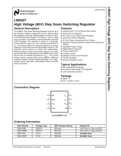
LM5007High Voltage (80V)Step Down Switching RegulatorGeneral DescriptionThe LM5007Step Down Switching Regulator features all of the functions needed to implement low cost,efficient,Buck bias regulators.This high voltage regulator contains an 80V,0.7A N-Channel Buck Switch.The device is easy to apply and is provided in the MSOP-8and the thermally enhanced LLP-8packages.The regulator is based on a hysteretic control scheme using an on time inversely proportional to V IN .This feature allows the operating frequency to remain relatively constant with load and input voltage variations.The hysteretic control requires no control loop compensation,while providing very fast load transient response.An intelli-gent current limit is implemented in the LM5007with forced off time that is inversely proportional to V OUT .This current limiting scheme reduces load current foldback.Additional protection features include:Thermal Shutdown,Vcc under-voltage lockout,gate drive undervoltage lockout,and Max Duty Cycle limiter.Featuresn Integrated 80V,0.7A N-Channel Buck Switch n Internal HV Vcc Regulatorn No Control Loop Compensation Required n Ultra-Fast Transient Responsen On Time Varies Inversely with Line Voltagen Operating Frequency Nearly Constant with Varying Line Voltagen Adjustable Output Voltage n Highly Efficient Operation n Precision Reference n Low Bias Currentn Intelligent Current Limit Protection n Thermal ShutdownnExternal Shutdown ControlTypical Applicationsn Non-Isolated Buck Regulatorn Secondary High Voltage Post Regulator n +42V Automotive SystemsPackagen MSOP -8n LLP -8(4mm x 4mm)Connection Diagram200783028-Lead MSOP,LLPOrdering InformationOrder Number Package Type NSC Package Drawing Supplied AsLM5007MM MSOP-8MUA08A 1000Units on Tape and Reel LM5007MMX MSOP-8MUA08A 3500Units on Tape and Reel LM5007SD LLP-8SDC08A Available Soon LM5007SDXLLP-8SDC08AAvailable SoonJanuary 2004LM5007High Voltage (80V)Step Down Switching Regulator©2004National Semiconductor Corporation Typical Application Circuit and Block Diagram20078301L M 5007 2Pin DescriptionPIN NAME DESCRIPTION APPLICATION INFORMATION 1SW Switching Node Power switching node.Connect to the LC outputfilter.2BST Boost Boot–strap capacitor input An external capacitor is required between the BSTand the SW pins.A0.01uF ceramic capacitor isrecommended.An internal diode between Vcc andBST completes the Buck gate drive bias network.3R CL Current Limit OFF time programming pinToff=10-5/(0.59+(FB/7.22x10−6x R CL))A resistor between this pin and RTN determines the variation of off time,along with the FB pin voltage, per cycle while in current limit.The off time is preset to17uS if FB=0V and decreases as the FB pin voltage increases.4RTN Circuit Ground5FB Feedback Signal from Regulated Output This pin is connected to the inverting input of theinternal regulation comparator.The regulationthreshold is2.5V.6R ON On time set pinTon=1.42x10⁻¹⁰R ON/Vin A resistor between this pin and Vin sets the switch on time as a function of Vin.The minimum recommended on time is300ns at the maximum input voltage.7Vcc Output from the internal high voltage biasregulator.V CC is nominally regulated to7Volts.If an auxiliary voltage is available to raise the voltage on this pin,above the regulation setpoint (7V),the internal series pass regulator will shutdown,reducing the IC power dissipation.Do not exceed14V.This output provides gate drive power for the internal Buck switch.An internal diode is provided between this pin and the BST pin.A local 0.1uF decoupling capacitor is recommended.Series pass regulator is current limited to10mA.8Vin Input supply voltage Recommended operating range:9V to75VLM50073Absolute Maximum Ratings (Note 1)If Military/Aerospace specified devices are required,please contact the National Semiconductor Sales Office/Distributors for availability and specifications.V IN to GND 80V BST to GND94V SW to GND (Steady State)-1VESD Rating (Note 5)Human Body Model 2kV Machine Model 200V BST to V CC80V BST to SW 14V V CC to GND14V All Other Inputs to GND-0.3to 7V Lead Temperature (Soldering 4sec)260˚CStorage Temperature Range-55˚C to +150˚COperating Ratings (Note 1)V IN9V to 75VJunction Temperature−40˚C to +125˚CElectrical CharacteristicsSpecifications with standard typeface are for T J =25˚C,and those with boldface type apply over full Operating Junction Temperature range .V IN =48V,unless otherwise stated (Note 3).Symbol ParameterConditionsMinTypMaxUnitsStartup Regulator V CC Reg V CC Regulator Output 6.677.4V V CC Current Limit(Note 4)11mAV CC SupplyV CC undervoltage Lockout Voltage (V CC increasing) 6.3V V CC Undervoltage Hysteresis 206mV V CC UVLO Delay (filter)3µs Operating Current (ICC)Non-Switching,FB =3V 500675µA Shutdown/Standby CurrentR ON =0V100200µASwitch CharacteristicsBuck Switch Rds(on)I TEST =200mA,VBST −VSW =6.3V (Note 6)0.741.34ΩGate Drive UVLO (VBST –VSW)Rising3.44.55.5V Gate Drive UVLO Hysteresis 400mV Breakdown Voltage V IN to Ground T J =25˚CT J =-40˚C to +125˚C 8076V Breakdown Voltage BST to V CCT J =25˚CT J =-40˚C to +125˚C8076VCurrent LimitCurrent Limit Threshold 535725900mA Current Limit Response Time I switch Overdrive =0.1A Time to Switch Off 225ns OFF time generator (test 1)FB=0V,RCL =100K 17µs OFF time generator (test 2)FB=2.3V,RCL =100K 2.65µs On Time GeneratorTON -1Vin =10V Ron =200K 2.15 2.77 3.5µs TON -2Vin =75V Ron =200K 290390490ns Remote Shutdown Threshold Rising0.450.7 1.1V Remote Shutdown Hysteresis40mVL M 5007 4Electrical Characteristics(Continued)Specifications with standard typeface are for T J=25˚C,and those with boldface type apply over full Operating Junction Temperature range.V IN=48V,unless otherwise stated(Note3).Symbol Parameter Conditions Min Typ Max Units Minimum Off TimeMinimum Off Timer FB=0V300ns Regulation and OV ComparatorsFB Reference Threshold Internal referenceTrip point for switch ON2.445 2.5 2.550VFB Over-Voltage Threshold Trip point for switch OFF 2.875VFB Bias Current100nA Thermal ShutdownTsd Thermal Shutdown Temp.165˚C Thermal Shutdown Hysteresis25˚C Thermal ResistanceθJA Junction to Ambient MUA Package200˚C/WSDC Package40˚C/WNote1:Absolute Maximum Ratings are limits beyond which damage to the device may occur.Operating Ratings are conditions under which operation of the device is intended to be functional.For guaranteed specifications and test conditions,see the Electrical Characteristics.Note2:For detailed information on soldering plastic MSOP and LLP packages,refer to the Packaging Data Book available from National Semiconductor Corporation.Note3:All limits are guaranteed.All electrical characteristics having room temperature limits are tested during production with T A=T J=25˚C.All hot and cold limits are guaranteed by correlating the electrical characteristics to process and temperature variations and applying statistical process control.Note4:The V CC output is intended as a self bias for the internal gate drive power and control circuits.Device thermal limitations limit external loading.Note5:The human body model is a100pF capacitor discharge through a1.5kΩresistor into each pin.The machine model is a200pF capacitor discharged directly into each pin.The machine model ESD compliance level for Pin5is150V.The human body ESD compliance level for Pin7and8is1000V.Note6:For devices procurred in the LLP-8package the Rds(on)limits are guaranteed by design characterization data only.Detailed Operating DescriptionThe LM5007Step Down Switching Regulator features all of the functions needed to implement low cost,efficient,Buck bias regulators.This high voltage regulator contains an80V, 0.7A N-Channel Buck Switch.The device is easy to apply and is provided in the MSOP-8and the thermally enhanced LLP-8packages.The regulator is based on a hysteretic control scheme using an on time inversely proportional to Vin.This feature allows the operating frequency to remain relatively constant with load and input voltage variations.The hysteretic control requires no control loop compensation, while providing very fast load transient response.An intelli-gent current limit scheme is implemented in the LM5007with forced off time,after current limit detection,which is in-versely proportional to Vout.This current limiting scheme reduces load current foldback.Additional protection features include:Thermal Shutdown,Vcc undervoltage lockout,Gate drive undervoltage lockout and Max Duty Cycle limiter.The LM5007can be applied in numerous applications to effi-ciently regulate step down higher voltage inputs.This regu-lator is well suited for48Volt Telcom and the new42V Automotive power bus ranges.Hysteretic Control Circuit OverviewThe LM5007is a Buck DC-DC regulator that uses an on time control scheme.The on time is programmed by an external resistor and varies inversely with line input voltage(Vin).The core regulation elements of the LM5007are the feedback comparator and the on time one-shot.The regulator output voltage is sensed at the feedback pin(FB)and is compared to an internal reference voltage(2.5V).If the FB signal is below the reference voltage,the buck switch is turned on fora fixed time pulse determined by the line voltage and aprogramming resistor(R ON).Following the on period theswitch will remain off for at least the minimum off timer periodof300ns.If the FB pin voltage is still below the referenceafter the300ns off time,the switch will turn on again foranother on time period.This switching behavior will continueuntil the FB pin voltage reaches the reference voltage level.The LM5007operates in discontinuous conduction mode atlight load currents or continuous conduction mode at heavierload currents.In discontinuous conduction mode,currentthrough the output inductor starts at zero and ramps up to apeak value during the buck switch on time and then back tozero during the off time.The inductor current remains at zerountil the next on time period starts when FB falls below theinternal reference.In discontinuous mode the operating fre-quency can be relatively low and will vary with load.There-fore at light loads the conversion efficiency is maintained,since the switching losses decrease with the reduction inload current and switching frequency.The approximate dis-continuous mode operating frequency can be calculated asfollows:In continuous conduction mode,current flows continuouslythrough the inductor and never ramps down to zero.In thismode the operating frequency is greater than the discontinu-ous mode frequency and remains relatively constant withload and line variations.The approximate continuous modeoperating frequency can be calculated as follows:LM50075Hysteretic Control Circuit Overview (Continued)The output voltage (Vout)can be programmed by two exter-nal resistors as shown in Figure 1.The regulation point can be calculated as follows:V OUT =2.5x (R1+R2)/R2The feedback comparator in hysteretic regulators depend upon the output ripple voltage to switch the output transistor on and off at regular intervals.In order for the internal comparator to respond quickly to changes in output voltage,proportional to inductor current,a minimum amount of ca-pacitor Equivalent Series Resistance (ESR)is required.A ripple voltage of 25mV to 50mV is recommended at the feedback pin (FB)for stable operation.In cases where the intrinsic capacitor ESR is too small,additional series resis-tance may be added.For applications where lower output voltage ripple is re-quired the load can be connected directly to the low ESRoutput capacitor,as shown in Figure 1.The series resistor (R)will degrade the load regulation.Another technique for enhancing the ripple voltage at the FB pin is to place a capacitor in parallel with the feedback divider resistor R1.The addition of the capacitor reduces the attenuation of the ripple voltage from the feedback dividerHigh Voltage Bias RegulatorThe LM5007contains an internal high voltage bias regulator.The input pin (Vin)can be connected directly to line voltages from 9to 75Volts.To avoid supply voltage transients due to long lead inductances on the input pin (Vin Pin 8),it is always recommended to connect low ESR ceramic chip capacitor ()0.1µF)between "Vin"pin and "RTN"pin (pin 4),located close to LM5007.The regulator is internally current limited to 10mA.Upon power up,the regulator is enabled and sources current into an external capacitor connected to the Vcc pin.When the voltage on the Vcc pin reaches the regulation point of 7V,the controller output is enabled.An external auxiliary supply voltage can be applied to the Vcc pin.If the auxiliary voltage is greater than 7Volts the internal regulator will essentially shutoff,thus reducing inter-nal power dissipation.20078305FIGURE 1.Low Ripple Output ConfigurationL M 5007 6High Voltage Bias Regulator(Continued)Over-Voltage ComparatorThe over-voltage comparator is provided to protect the out-put from overvoltage conditions due to sudden input line voltage changes or output loading changes.The over-voltage comparator monitors the FB pin versus an internal 2.875V reference(OV_REF).If the voltage at FB rises above OV_REF the comparator immediately terminates the buck switch on time pulse.ON Time generator and Shutdown The on time of the LM5007is set inversely proportional to the input voltage by an external resistor connected between Ron and Vin.The Ron terminal is a low impedance input biased at approximately1.5V.Thus the current through the resistor and into the Ron terminal is approximately propor-tional to Vin and used internally to control the on timer.This scheme of input voltage feed-forward hysteretic operation achieves nearly constant operational frequency over varying line and load conditions.The on time equation for the LM5007is:Ton=1.42x10⁻¹⁰x R ON/V INThe R ON pin of the LM5007also provides a shutdown func-tion which disables the regulator and significantly decreases quiescent power dissipation.By pulling the R ON pin to below 0.7V logic threshold activates the low power shutdown mode.The V IN quiescent current in the shutdown mode is approximately100µA internal to the LM5007plus the current in the R ON resistor.20078306FIGURE2.Self Biased ConfigurationLM50077ON Time generator and Shutdown(Continued)Current LimitThe LM5007contains an intelligent current limit off timer intended to reduce the foldback characteristic inherent with fixed off-time over-current protection.If the current in the Buck switch exceeds 725mA the present cycle on time is immediately terminated (cycle by cycle current limit).Follow-ing the termination of the cycle a non-resetable current limit off timer is initiated.The duration of the off time is a function of the external resistor (R CI )and the FB pin voltage.When the FB pin voltage equals zero,the current limit off time is internally preset to 17uS.This condition occurs in short circuit operation when a maximum amount of off time is required.In cases of overload (not complete short circuit)the current limit off time can be reduced as a function of the output voltage (measured at the FB pin).Reducing the off time with smaller overloads reduces the amount of foldback and also reduces the initial start-up time.The current limit off time for a given FB pin voltage and R CI resistor can be calculated by the following equation:Toff =10-5/(0.59+(V FB /7.22x 10-6x R CL ))Applications utilizing low resistance inductors and/or a low voltage drop rectifier may require special evaluation at high line,short circuit conditions.In this special case the preset 17uS (FB =0V)off time may be insufficient to balance the inductor volt*time product.Additional inductor resistance,output resistance or a larger voltage drop rectifier may be necessary to balance the inductor cycle volt*time product and limit the short circuit current.N -Channel Buck Switch and DriverThe LM5007integrates an N-Channel Buck switch and as-sociated floating high voltage gate driver.This gate driver circuit works in conjunction with an external bootstrap ca-pacitor and an internal high voltage diode.The bootstrapcapacitor is charged by V CC through the internal high voltage diode.A 0.01uF ceramic capacitor connected between the BST pin and SW pin is recommended.During each cycle when the Buck switch turns off,the SW pin is approximately 0V.When the SW pin voltage is low,the bootstrap capacitor will be charged from Vcc through the internal diode.The minimum off timer,set to 300ns,ensures that there will be a minimum interval every cycle to recharge the bootstrap capacitor.An external re-circulating diode from the SW pin to ground is necessary to carry the inductor current after the internal Buck switch turns off.This external diode must be of the Ultra-fast or Schottky type to reduce turn-on losses and current over-shoot.The reverse voltage rating of the re-circulating diode must be greater than the maximum line input voltage.Thermal ProtectionInternal Thermal Shutdown circuitry is provided to protect the integrated circuit in the event the maximum junction tem-perature is exceeded.When thermal protection is activated,typically at 165degrees Celsius,the controller is forced into a low power reset state,disabling the output driver.This feature is provided to prevent catastrophic failures from ac-cidental device overheating.20078307FIGURE 3.Shutdown ImplementationL M 50078Operational Waveforms20078308LM5007Operation:V OUT=10V,V IN=20V,I OUT=250mA CH1:Switch Node,CH2:V OUT(AC),CH4:Inductor CurrentFIGURE4.Operational Waveforms20078309LM5007Operation:V OUT=10V,V IN=75V,I OUT=250mA CH1:Switch Node,CH2:V OUT(AC),CH4:Inductor CurrentFIGURE5.LM500710V Output Efficiency20078310FIGURE6.Current Limit V FB vs T OFFR CL=50k-600k20078311FIGURE7.V IN vs T ONR ON=100k,200k,300k20078312FIGURE8.LM5007910V,400mA Demo Board Bill of MaterialsITEM PART NUMBER DESCRIPTION VALUE C1C4532X7R2A105M CAPACITOR,CER,TDK 1µ,100V C2C4532X7R1E156M CAPACITOR,CER,TDK 15µ,25V C3C1206C104K5RAC CAPACITOR,CER,KEMET 0.1µ,50V C4C1206C103K5RAC CAPACITOR,CER,KEMET 0.01µ,50V C5C3216X7R2A104KTCAPACITOR,CER,TDK 0.1µ,100VD1MURA110T3DIODE,100V,ON SEMI L1SLF7045T-101MR60-1BUCK INDUCTOR,TDK100µH R1CRCW12062003F RESISTOR 200K R2CRCW12061003F RESISTOR 100K R3CRCW12063011F RESISTOR 3.01K R4CRCW12061001F RESISTOR 1K R5CRCW12061R00FRESISTOR1U1LM5007REGULATOR,NATIONALL M 5007 10LM5007 Physical Dimensions inches(millimeters)unless otherwise noted8-Lead MSOP PackageNS Package Number MUA08A11Physical Dimensionsinches (millimeters)unless otherwise noted (Continued)8-Lead LLP PackageNS Package Number SDC08ALIFE SUPPORT POLICYNATIONAL’S PRODUCTS ARE NOT AUTHORIZED FOR USE AS CRITICAL COMPONENTS IN LIFE SUPPORT DEVICES OR SYSTEMS WITHOUT THE EXPRESS WRITTEN APPROVAL OF THE PRESIDENT AND GENERAL COUNSEL OF NATIONAL SEMICONDUCTOR CORPORATION.As used herein:1.Life support devices or systems are devices or systems which,(a)are intended for surgical implant into the body,or (b)support or sustain life,and whose failure to perform when properly used in accordance with instructions for use provided in the labeling,can be reasonably expected to result in a significant injury to the user. 2.A critical component is any component of a life support device or system whose failure to perform can be reasonably expected to cause the failure of the life support device or system,or to affect its safety or effectiveness.BANNED SUBSTANCE COMPLIANCENational Semiconductor certifies that the products and packing materials meet the provisions of the Customer Products Stewardship Specification (CSP-9-111C2)and the Banned Substances and Materials of Interest Specification (CSP-9-111S2)and contain no ‘‘Banned Substances’’as defined in CSP-9-111S2.National Semiconductor Americas Customer Support CenterEmail:new.feedback@ Tel:1-800-272-9959National SemiconductorEurope Customer Support CenterFax:+49(0)180-5308586Email:europe.support@Deutsch Tel:+49(0)6995086208English Tel:+44(0)8702402171Français Tel:+33(0)141918790National Semiconductor Asia Pacific Customer Support CenterEmail:ap.support@National SemiconductorJapan Customer Support Center Fax:81-3-5639-7507Email:jpn.feedback@ Tel:81-3-5639-7560L M 5007H i g h V o l t a g e (80V )S t e p D o w n S w i t c h i n g R e g u l a t o rNational does not assume any responsibility for use of any circuitry described,no circuit patent licenses are implied and National reserves the right at any time without notice to change said circuitry and specifications.。