
ALLEGROPCBLAYOUT教程
- 格式:ppt
- 大小:349.00 KB
- 文档页数:22


Allegro教程一基本功能1.1 焊盘制作目的:制作SMD焊盘、通孔焊盘以及过孔工具:Pad Designer窗口功能解析:Summary(设计简介)Unites:设置单位(mils/inch/mm/…)Decimal places(设计精度)Usage optionsMicorvia(微孔,用于忙埋孔设计)Suppress unconnected int. pads;legacy artwork(除去未连接层的焊盘)Mech pins use antipads as Route Keepout;ARKMultiple drill(多孔焊盘)Staggered(钻孔是错列)Rows(行数)Columns(列数)ClearanceX(X轴间隔)ClearanceY(Y轴间隔)Drill/Slot holeHole type(Circle/Oval Slot/Rectangle Slot)Plating(Plated/Non-Plated/Optional)Non-standard drill——Laser(激光钻孔)——Plasma(电浆钻孔)——Punch(冲击钻孔)——Wet/dry(湿干蚀刻)——Photo Imaging(照片成相)——Conductive lnk Formation(油墨传导构造)——OtherDrill/Slot symbolFigure (钻孔符号形状)Characters(图形内文字)Top viewPadstack layerssingle layer mode(单层焊盘)ViewsRegular Pad(正规焊盘)Thermal Relief(热风焊盘,一般比Regular大20mil)Anti Pad(隔离焊盘,一般比Regular大20mil)——Geometry(焊盘形状)——Shape(用于不规则焊盘,除了热风焊盘)——Flash(专用于热风焊盘)二PCB封装库制作目的:制作SMD焊盘、通孔焊盘以及过孔工具:Pad Editor步骤解析:1 进入PCB封装库编辑环境file→new→(封装命名/选择Package symbol/Package symbol(wizard)ok 2 设置合适的编辑环境setup→design parameter editorconnect point size(T点尺寸设置)DRC maker size(DRC符号大小设置)Rat T(Virtual pin) size(设定T点飞线的大小)Max rband count(设定元件最多飞线显示数目)Ratsnest geometry(设定飞线的布线模式)——Jogged(飞线自动显示有拐角)——Straight(飞线显示最短直线段)Ratsnest points——Closest endpoint(飞线显示最近的连接点)——PIN to PIN(飞线显示焊盘到焊盘)-Display net name(OpenGL only)——Clines/Shapes/PinsEnhanced display modes(高亮模式)Setup Grids(栅格设置)——Non-Etch(非走线层)/All Etch(走线层)/TOP(顶层)/BOTTOM(底层)User Units(环境单位)Size(尺寸)Accuracy(精度)Long Name Size(名字大小限制)Extents(面板尺寸)move origin(设置零点坐标,自动清零)Drawing type(设置编辑类型)Jumper(设置跳线,单面板常用)Line lock(拉线型态)——Lock direction(off/45/90)——Lock mode(Line/Arc) ——Minimum radius(最小半径)——Fixed 45 Length——Fixed radiusVoid controls——Aperture for artwork chk(设置小于定值的shape不会被显示)——Susppress shapes less than(设置去除碎铜阈值)——Clearances设置静态铜对各种元素的避让距离——Create pin voids(平滑PIN脚间因覆铜产生的尖角)——Trim Control(设置锐角处理方式)Clearances(设置避让元素距离)Thermal relief connects(设置散热连接方式)Route(默认Add Connect Option设置)layer mode——Alternate Subclass——Working Layers(针对HDI板,显示etch/conductor走线层)Route Offset(实现特殊角度走线)Miter(拐角长度)Bubble——Off——Hug only——Hug preferred——Shove preferredShove vias——Off——Minimal 最小幅度推挤via ——Full 完全地推挤viaGridless 控制是否移动到格点上Clip dagling clines 推挤小段走线效果Smooth——Off——Minimal——FullSnap to connect point 自动吸附上接点Replace etch 自动消除旧的走线回路Route(Slide默认设置)Min Corner Size 在45度转折角情况下,允许在2条非平行线段之间的最小线宽度Min Arc Radius 在弧线调整控制下,能够设定两相邻线段间的弧线最小半径Vertex Action 除了动节点外,增加了变换为直线以及弧线转角Allow DRCs 允许DRC接入管理Auto Join 推线段时,透过此功能选项将平行相接的线段一起加入推线Extend selection 透过此功能能令选择的线段与其左右相邻线段固定转折角度何长度进行调整3 添加焊盘layout→pin——connect 有编号的焊盘——mechanical 无编号的焊盘4 放置元件实体区域(Place_Bound)Setup→Areas→Package Boundary元件封装区域5 设定元件限高Setup→Areas→Package Height6 设计元件丝印层(Silkscreen_)7 设计元件装配层(Assembly_)元件实体区域保守建议Place_Bound与Assembly_*保持一致8 设计元件标示符Layout→Labels→RefDef(通常#REFDES放在Assembly_*层)Layout→Labels→Value(通常#VALUE放在Silkscreen_*层)更改字符Edit→Change→(option设置)→选中对应的text。
26、非电气引脚零件的制作1、建圆形钻孔:(1)、parameter:没有电器属性(non-plated)(2)、layer:只需要设置顶层和底层的regular pad,中间层以及阻焊层和加焊层都是null。
注意:regular pad要比drill hole大一点27、Allegro建立电路板板框步骤:1、设置绘图区参数,包括单位,大小。
2、定义outline区域3、定义route keepin区域(可使用Z-copy操作)4、定义package keepin区域5、添加定位孔28、Allegro定义层叠结构对于最简单的四层板,只需要添加电源层和底层,步骤如下:1、Setup –> cross-section2、添加层,电源层和地层都要设置为plane,同时还要在电气层之间加入电介质,一般为FR-43、指定电源层和地层都为负片(negtive)4、设置完成可以再Visibility看到多出了两层:GND和POWER5、铺铜(可以放到布局后再做)6、z-copy –> find面板选shape(因为铺铜是shape)–> option面板的copy to class/subclass选择ETCH/GND(注意选择create dynamic shape)完成GND层覆铜7、相同的方法完成POWER层覆铜Allegro生成网表1、重新生成索引编号:tools –> annotate2、DRC检查:tools –> Design Rules Check,查看session log。
3、生成网表:tools –> create netlist,产生的网表会保存到allegro文件夹,可以看一下session log内容。
29、Allegro导入网表1、file –> import –> logic –> design entry CIS(这里有一些选项可以设置导入网表对当前设计的影响)2、选择网表路径,在allegro文件夹。

Allegro给各种形式的板框导弧操作指导Allegro可以给板框导弧,让加工出来的板框更加圆滑,具体操作步骤如下1.板框是line形式的2.选择Manufacture-Drafting-Fillet命令3.在Options里面Radius输出导弧的半径,比如78.744.框选两个线段的部分5.完成后的效果如下图6.框选4个角落,形成圆弧的板框7.如果板框是shape形式的,这个命令就不起作用了8.按照下面的步骤进行,shape-decompose shape9.Option里面还是选择到outline层,并选择delete shape afterdecompose10.Find处的勾选shapes11.框选整个板框12.可以看到板框就变成line形式的了13.然后重复上面的步骤,Manufacture-Drafting-Fillet命令得到一个圆弧的板框但是要注意由于已经变成了分离的线段,需要逐段点击才行14.然后把板框变回shape形式,操作如下,选择outline层,选择lines15.框选整个板框16.删除line形式的板框。
按删除命令,find只选择lines,框选整个板框17.留下一个shape形式并且弧形的板框This section is describe what the function allegro have ,helpfully could let user know more about allegroAllegro Design and Analysis includes design authoringPCB layout and Library and Design Data ManagementWith. It can ensure the end-to-end design of PCB with high quality and efficiencyRealize smooth data transfer between tools, shorten PCB design cycle, and shorten productMarket time1. Design authoringProvide a flexible logic constraint driven flow, management design rules, network hierarchy,Bus and differential pair.1.1.1 Main features and functionsThrough hierarchical and design "derivation" function, improve the original of complex designMap editing efficiency.Powerful CIS helps users quickly determine part selection and accelerate design flowAnd reduce project cost.1.2.1 Main featuresSchematic designers and PCB design engineers can work in parallel. Advanced design efficiency improves functions, such as copying the previous schematic design Select multiplexing with or by page. Seamless integration into pre simulation and signal analysis.1.2.2 Main FunctionsProvide schematic diagram and HDL/Verilog design input.Assign and manage high-speed design rules.Support netclasses, buses, extension networks and differential pairs. Powerful library creation and management functions.Allows synchronization of logical and physical designs.Realize multi-user parallel development and version control.Pre integration simulation and signal analysis.Support customizable user interface and enterprise customization development.1.3 o Allegro n Design Publisher1.3.1 Main Features and FunctionsAllows you to share designs with others using PDF files.The entire design is represented in a single, compact PDF format. Improve design readability.Provide content control - users can select the content to be published.1.4 Allegro A FPGA m System Planner1 1.4.1 Main features and functionsComplete and scalable FPGA/PCB collaborative design technology for ideal "Design and correct "pin assignment.Scalable FPGA/PCB protocol from OrCAD Capture to Allegro GXLSame as the design solution.Shorten the optimization pin allocation time and accelerate the PCB design cycle.2. B PCB layoutIt provides expandable and easy to use PCB design (including RFPCB)Then drive PCB design solution. It also includes innovative new automatic deliveryMutual technology can effectively improve the wiring of high-speed interfaces; Apply EDMD (IDX) mode, which makes ECAD/MCAD work smoothly; Execute modern industry standard IPC-2581,Ensure that the design data is simply and high-quality transferred to the downstream link.2.1.1 Main featuresSpeed up the design process from layout, wiring to manufacturing. Including powerful functions, such as design zoning, RF design functions and global design rules Stroke.It can improve productivity and help engineers to quickly move up to mass production* g- M4 G8 |6 }9 k7 G2.1.2 Main FunctionsProvide scalable full function PCB design solutions.Enable constraint driven design processes to reduce design iterations. Integrated DesignTrueDFM technology provides real-time DFM inspection. Provide a single, consistent context for management.Minimize design iterations and reduce overall Flex and rigid flexible designCost, and has advanced rigid and flexible design functions.Realize dynamic concurrent team design capability, shorten design cycle, and greatly reduceTime spent in routing, winding and optimization.Provide integrated RF/analog design and mixed signal design environment. Provides interactive layout and component placement.Provide design partitions for large distributed development teams. Realize real-time, interactive push editing of routing.It is allowed to use dynamic copper sheet technology to edit and update in real time.Manage netscheduling, timing, crosstalk, routing by designated layer and area Bundle.Provide proven PCB routing technology for automatic routing.Realize hierarchical route planning and accelerate the completion of design.Shorten interconnect planning and cabling time for high-speed interface intensive design.Provide a comprehensive, powerful and easy-to-use tool suite to help designersEfficient and successful manufacturing switch: DFM Checker is aimed at the company/manufacturerReview the specific rules of manufacturing partners; Used to reduce manufacturing and assembly documentsThe document editing time of the file can reach 70%; The panel editorwill assemble the panel designThe intention is communicated to the manufacturing partners; Output design data in various manufacturing formats.3. y Library d and n Design a Data ManagementFor cost-effective projects that need to be delivered on time, it is easy to obtainCurrent component information and design data are critical. library and designData management is a collaborative control of the company's internal cooperation and design processAdvanced functions are provided. As the design cycle shortens and the complexity increases, youThere must be a design approach that increases predictability and accelerates design turnaround.3.1.1 Main featuresReduce time and optimize library development related resources. Improve the precision in the process of parts manufacturing. Q9 b3.1.2 Main functionsReduce time and optimize library development and validation through integrated creation and validation processes Certification related resources.A simple method to develop devices with large pin count can shorten the time from a few days to A few minutes.Powerful graphic editor supports custom shape and spreadsheet import forSchematic symbols are created to ensure the reliability and integrity of data.Supports the import of part information from general industry formats, allowing rapid creation and Update part information.Common library development environment supporting schematic tools from different suppliers, including Mentor Graphics Design Architect and Mentor Graphics Viewdraw。
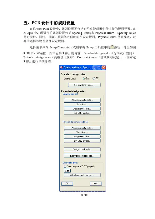
五、PCB设计中的规则设置在这节的PCB设计中,规则设置不包括对约束管理器中所进行的规则设置。
在Allegro中,所进行的规则设置包括Spacing Rules和Physical Rules:Spacing Rules 是对元件、网线、引脚、敷铜等之间的间距设定规则;Physical Rules是对线宽、过孔的选择等物理属性设定规则。
选择菜单命令Setup/Constraints或则单击Setup工具栏中的按钮,弹出如图8_38所示对话框。
图中包括3部分的内容:Standard design rules(标准设计规则)、Extended design rules(高级设计规则)、Constraint areas(区域规则设定)。
下面对这3部分进行详细介绍。
8_381、标准设计规则1)设定在线检查规则On-line DRC:设定是否实时检查DRC,On表示在线检查,Off表示关闭此功能,建议选择打开实时检查。
2)标准设计规则检查单击图8_38中的按钮,弹出默认规则设置对话框,如图8_39所示。
8_39在此对话框中,可以设定默认的间距规则如:线到线的最小间距、线到焊盘的最小间距以及焊盘到焊盘的最小间距等。
此处定义的规则是默认的规则,是处于最低优先级的规则设定。
2、高级设计规则——间距规则的设定1)设定间距规则值在图8_38所示的对话框中,单击Spacing rule set中的按钮,打开间距规则设定对话框,如图8_40所示。
在此对话框中,可以对所有走线层(选中ALL ETCH)或单独的一层(选择相应的层)来设定默认的间距规则如:引脚到引脚的最小规则、线到线的最小规则、过孔到过孔之间最小的间距规则。
在此还可以设定相同网名是否执行规则检查(Same Net DRC),其默认值是选择Off表示相同网名不执行规则检查,这里建议大家选择On表示对相同网名同样执行规则检查。
2)添加新的规则对整个印制电路板都使用DEFAULT(默认)的规则有时候不能满足用户的要求,在此可以输入新的规则来使用,以增加一个适合时钟信号的规则CLK为例来介绍添加方法。