基于TMS320F28335的雷达伺服系统的设计与实现
- 格式:pdf
- 大小:405.72 KB
- 文档页数:4
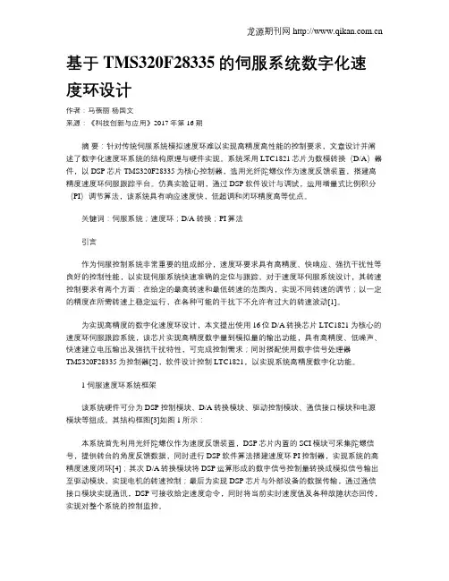
基于TMS320F28335的伺服系统数字化速度环设计作者:马蓓丽杨国文来源:《科技创新与应用》2017年第16期摘要:针对传统伺服系统模拟速度环难以实现高精度高性能的控制要求,文章设计并阐述了数字化速度环系统的结构原理与硬件实现。
系统采用LTC1821芯片为数模转换(D/A)器件,以DSP芯片TMS320F28335为核心控制器,选用光纤陀螺仪作为速度反馈装置,搭建高精度速度环伺服跟踪平台。
仿真实验证明,通过DSP软件设计与调试,运用增量式比例积分(PI)调节算法,该系统具有响应速度快,低超调和闭环精度高等优点。
关键词:伺服系统;速度环;D/A转换;PI算法引言作为伺服控制系统非常重要的组成部分,速度环要求具有高精度、快响应、强抗干扰性等良好的控制性能,以实现伺服系统快速准确的定位与跟踪。
对于速度环伺服系统设计,其转速控制要求有两个方面:在给定的最高转速和最低转速的范围内,实现不同转速的调节;以一定的精度在所需转速上稳定运行,在各种可能的干扰下不允许有过大的转速波动[1]。
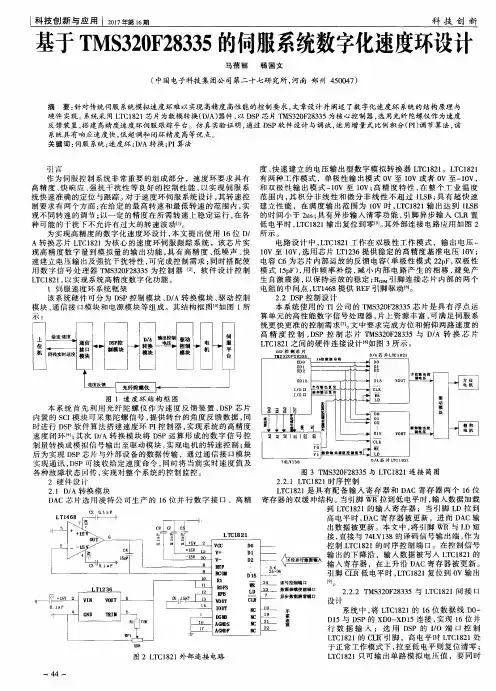
为实现高精度的数字化速度环设计,本文提出使用16位D/A转换芯片LTC1821为核心的速度环伺服跟踪系统,该芯片实现高精度数字量到模拟量的输出功能,具有高精度、低噪声、快速建立电压输出及强抗干扰特性,可完成控制需求;同时搭配使用数字信号处理器TMS320F28335为控制器[2],软件设计控制LTC1821,以实现系统高精度数字化功能。
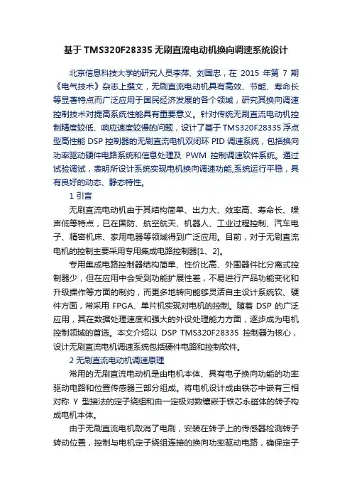
1 伺服速度环系统框架该系统硬件可分为DSP控制模块、D/A转换模块、驱动控制模块、通信接口模块和电源模块等组成。
其结构框图[3]如图1所示:本系统首先利用光纤陀螺仪作为速度反馈装置,DSP芯片内置的SCI模块可采集陀螺信号,提供转台的角度反馈数据,同时进行DSP软件算法搭建速度环PI控制器,实现系统的高精度速度闭环[4];其次D/A转换模块将DSP运算形成的数字信号控制量转换成模拟信号输出至驱动模块,实现电机的转速控制;最后为实现DSP芯片与外部设备的数据传输,通过通信接口模块实现通讯,DSP可接收给定速度命令,同时将当前实时速度值及各种故障状态回传,实现对整个系统的控制监控。
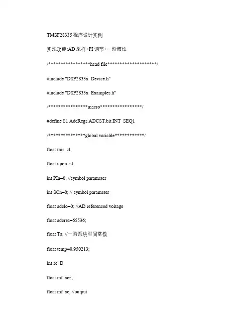
TMSF28335程序设计实例实现功能:AD采样+PI调节+一阶惯性/*****************head file********************/ #include "DSP2833x_Device.h"#include "DSP2833x_Examples.h"/****************macro*****************/#define S1 AdcRegs.ADCST.bit.INT_SEQ1/***************global variable************/float this_zl;float upon_zl;int PIn=0; //symbol parameterint SCn=0; // symbol parameterfloat adclo=0; //AD referenced voltagefloat adcres=65536;float Ta; //一阶系统时间常数float temp=0.950213;int sc_D;float mf_scz;float mf_sc; //outputunsigned int * Sda;float power_set;float power_get; // actual output voltagefloat KP_wr; //PI proportion coefficientfloat KI_wr; //PI integral coefficientfloat error_sg; //PI correlative parameterfloat error_1;float error_2;/****************function*******************/interrupt void cpu_timer0_isr(void;interrupt void ad_isr(void;void Init_Timer0(void;void Init_Xintf(void;void Init_Gpio(void; //GPIO initialization program void Initadc(void; //AD initialize float PI_T(float power_sd,float pow_in; //PI control functionvoid delay_ys(void; //delay subprogram/***************main function**********************/void main(void{unsigned int * Sda =(unsigned int * 0x200000; //define DA address,XINTF Zone7 InitSysCtrl(; // initialize system subprogramInit_Timer0(;DINT;InitPieCtrl(;IER=0x0000;IFR=0x0000;InitPieVectTable(;Init_Gpio(;Initadc(;Init_Xintf(;CpuTimer0Regs.TCR.bit.TIE=1;EALLOW; // 解除寄存器保护PieVectTable.TINT0=&cpu_timer0_isr; //用CUP_Timer0中断函数入口更新//PIE向量表PieVectTable.ADCINT=&ad_isr; //用AD中断函数更新PIE向量表EDIS; //使能寄存器保护ConfigCpuTimer(&CpuTimer0,150,500; //timing 500usStartCpuTimer0(;PieCtrlRegs.PIEIER1.all=0x60; //使能PIE内的CUP_Timer0和AD //中断IER |=0x0001; // 使能CPU INT 1EINT;}*****************CPU timerinitialization***********************************void Init_Timer0(void{CpuTimer0Regs.PRD.all=75000; //set timer period timing:500usCpuTimer0Regs.TPR.all=0;CpuTimer0Regs.TPRH.all=0;//CpuTimer0Regs.TCR.bit.TSS=1; //stop timer}********************A/Dinitialization**********************************void Initadc(void{long i; //AD initializeAdcRegs.ADCTRL1.bit.RESET=1;for(i=0;i<100;i++ {};AdcRegs.ADCTRL1.bit.RESET=0;AdcRegs.ADCTRL1.bit.SUSMOD=0;AdcRegs.ADCTRL1.bit.ACQ_PS=0; //setting sample windowAdcRegs.ADCTRL1.bit.CPS=0;AdcRegs.ADCTRL1.bit.CONT_RUN=0; //启动-停止模式AdcRegs.ADCTRL1.bit.SEQ_CASC=0; //AdcRegs.ADCTRL3.bit.ADCBGRFDN=3; //给ADC模块的内部基准电路上电for(i=0;i<400000;i++ {}; //delay more than 7msAdcRegs.ADCTRL3.bit.ADCPWDN=1; //给ADC模块的其余模拟电路上电for(i=0;i<10000;i++ {}; //delay more than 20usAdcRegs.ADCTRL3.bit.ADCCLKPS=10;AdcRegs.ADCTRL3.bit.SMODE_SEL=0; //choose sample styleAdcRegs.ADCMAXCONV.all=0x0000;AdcRegs.ADCCHSELSEQ1.bit.CONV00=0x0000;AdcRegs.ADCST.bit.INT_SEQ1_CLR=1;AdcRegs.ADCTRL2.bit.RST_SEQ1=1; //复位排序器1AdcRegs.ADCTRL2.bit.INT_ENA_SEQ1=1; //SEQ1 interruptAdcRegs.ADCTRL2.bit.INT_MOD_SEQ1=0; //choose interrupt style }*********************external peripheralsinitialization****************************** void Init_Xintf(void {EALLOW;XintfRegs.XINTCNF2.bit.XTIMCLK=1;XintfRegs.XTIMING6.bit.XWRLEAD=3;XintfRegs.XTIMING6.bit.XWRACTIVE=7;XintfRegs.XTIMING6.bit.XWRTRAIL=3;XintfRegs.XTIMING6.bit.XRDLEAD=3;XintfRegs.XTIMING6.bit.XRDACTIVE=7;XintfRegs.XTIMING6.bit.XRDTRAIL=3;XintfRegs.XTIMING6.bit.X2TIMING=0;EREADY=0;XintfRegs.XTIMING6.bit.XSIZE=3;EDIS;}********************************I/Oinitialization******************************* void Init_Gpio(void {EALLOW; //GPIO initializeGpioCtrlRegs.GPBMUX1.all=0xFFFFFC00; //设置B口为地址线以及DAC片选信号GpioCtrlRegs.GPCMUX1.all=0xFFFFFFFF; //set C Port as date addressGpioCtrlRegs.GPAMUX1.all=0x0000;GpioCtrlRegs.GPADIR.all= 0x0003;GpioDataRegs.GPADA T.all= 0x0003;GpioDataRegs.GPACLEAR.all= 0x0003; //choose GPIO1,2 as DA signal address EDIS;}****************************PIfunction****************************************** portal parameter:power_sd and pow_inexport parameter:this_zlfloat PI_T(float power_sd,float power_in{error_1 = error_sg;error_sg = power_sd - power_in;error_2 = error_sg - error_1;if(PIn == 0{error_2 = 4.0; //avoid error_2 too largePIn++;}this_zl = KP_wr*error_sg + KI_wr*error_2;error_sg = error_1;return this_zl;}*******************************Delayfunction*********************************** void delay_ys(void {long i;for(i=0;i<100000;i++ {};}*************************timer 0 interrupt dealfunction***********************interrupt void cpu_timer0_isr(void{DINT;StopCpuTimer0(;CpuTimer0Regs.TCR.bit.TIF=1; //清CPU定时器0的中断标志PieCtrlRegs.PIEACK.all |=0x0001; //使能第一组中断以使AD产生的中断能// 被CPU响应AdcRegs.ADCTRL2.bit.SOC_SEQ1=1; //使能排序器,启动AD转换EINT;while(S1==0 {}; //等待AD转换的完成delay_ys(;}************************AD interruptfunction*********************************interrupt void ad_isr(void{DINT;AdcRegs.ADCTRL2.bit.RST_SEQ1=1;power_get=((floatAdcRegs.ADCRESULT0*3.0/adcres + adclo; //对采样数据进行转换if(SCn == 0{mf_scz = 2.5;SCn++;}mf_sc=mf_scz;upon_zl=PI_T( power_get, mf_sc; //调用PI环节的函数mf_sc=1/Ta * upon_zl * temp; //通过一阶惯性环节的处理delay_ys(;mf_scz=mf_sc;sc_D=(int(mf_sc * 4096/5;* (Sda = sc_D; //写数据到DA的数据线AdcRegs.ADCST.bit.INT_SEQ1_CLR=1; PieCtrlRegs.PIEACK.all |=0x0001; //使能第一组中断EINT;StartCpuTimer0(; //启动定时器0,开始下一次采样}。
MS320F28335及其最小应用系统设计TMS320F28335型数字信号处理器是TI公司的一款TMS320C28X系列浮点DSP控制器。
与以往的定点DSP相比,该器件的精度高,成本低,功耗小,性能高,外设集成度高,数据以及程序存储量大,A/D转换更精确快速等。
它采用内部供电,外部供电,因而功耗大大降低。
且主频高达150 MHz,处理速度快,是那些需要浮点运算便携式产品的理想选择。
2 TMS320F28335简介TMS320F28335采用176引脚LQFP四边形封装。
其主要性能如下:高性能的静态CMOS技术,指令周期为ns,主频达150MHz;高性能的32位CPU,单精度浮点运算单元(FPU),采用哈佛流水线结构,能够快速执行中断响应,并具有统一的内存管理模式,可用C/C++语言实现复杂的数学算法;6通道的DMA控制器;片上256K(64K)*l6的Flash存储器,34K(18K)*l6的SARAM存储器.1K*16 OT PROM和8K(4K)*l6的Boot ROM。
其中Flash,OTPROM,16K*l6的SARAM均受密码保护;带()的为2808控制时钟系统具有片上振荡器,看门狗模块,支持动态PLL调节,内部可编程锁相环,通过软件设置相应寄存器的值改变CPU的输入时钟频率;8个外部中断,相对TMS320F281X系列的DSP,无专门的中断引脚。
GPIO0~ GPIO63连接到该中断。
GPI00-GPI031连接到XINTl,XINT2及XNMI外部中断,G Pl032~GPI063连接到XINT3-XINT7外部中断;支持58个外设中断的外设中断扩展控制器(PIE),管理片上外设和外部引脚引起的中断请求;增强型的外设模块:18个PWM输出,包含6个高分辨率脉宽调制模块(HRP WM)、6个事件捕获输入,2通道的正交调制模块(QEP);3个32位的定时器,定时器0和定时器1用作一般的定时器,定时器0接到P IE模块,定时器1接到中断INTl3;定时器2用于DSP/BIOS的片上实时系统,连接到中断INTl4,如果系统不使用DSP/BIOS,定时器2可用于一般定时器;串行外设为2通道CAN模块、3通道SCI模块、2个McBSP(多通道缓冲串行接口)模块、1个SPI模块、1个I2C主从兼容的串行总线接口模块;12位的A/D转换器具有16个转换通道、2个采样保持器、内外部参考电压,转换速度为80 ns,同时支持多通道转换;88个可编程的复用GPIO引脚;低功耗模式;1.9 V内核,3.3 V I/O供电;符合IEEEll49.1标准的片内扫描仿真接口(JTAG);TMS320F28335的存储器映射需注意以下几点:片上外设寄存器块0~3只能用于数据存储区,用户不能在该存储区内写入程序。
www�ele169�com | 47信息工程硬件电路结构以及软件控制算法设计。
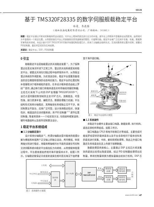
1 稳定平台系统组成■1.1 分轴稳定简介设计采用分轴稳定[8]。
所谓分轴稳定是对载体的摇摆分解为横摇和纵摇两个正交轴上的独立运动,再对横摇、纵摇两轴分别进行稳定。
用载体两轴相对水平面的误差信号控制交流伺服系统向稳定平台施加反方向转矩,从而使载体摇摆过程中,平台基准面始终相对海平面保持水平,如图1所主支柱减速器横摇机构纵摇机构伺服电机yα■1.2 系统硬件本稳定平台硬件主要由接口电路、数据处理、执行机构、姿态反馈机构等组成,如图2所示。
接口电路由CPLD 和电平转换芯片等组成,主要完成对舰船罗经提供的载体姿态以及平台自身相对于载体坐标系的姿态进行采集、中转、解码和预处理等。
除此之外接口电路还负责将姿态信息上传便于观察数据。
数据处理是系统核心,主要通过DSP 主控芯片将采集到的姿态比较得出角度误差,经过PID 控制器处理得出控芯林青,韦在陆(桂林长海发展有限责任公司,广西桂林,541001)摘要:稳定平台通过不断地采集载体的运动姿态,对平台上物体的姿态进行反方向补偿,使平台上的物体不受载体运动的影响,始终相对水平面保持一个既定位置。
从而使安装在平台上的装备能实现快速精准的跟踪、扫描等功能。
稳定平台被广泛应用于车载、机载、舰载等军事和民用领域。
本设计基于DSP TMS320F28335数字伺服控制处理芯片,采用了分轴稳定结构形式、交流伺服系统位置环控制、增量式PID控制器。
最后将呈现实际应用结果。
关键词:稳定平台;DSP;PID控制器48 | 电子制作 2020年12月PID 控制器基本的思想就是将偏差的比例(P)、积分(I)和微分(D)通过线性组合构成控制量,用该控制量对被控对象进行控制。
其中比例环节成比例地反应控制系统的偏差信号,保证系统的快速性;积分环节主要用于消除静态误差,提高系统的置位精度;微分环节能反映偏差信号的变化趋势,并在偏差信号变得过大或过小之前,在系统中提前引入一个修正信号,从而加快系统的动作速度,缩短调节时间。
基于TMS320F28335无刷直流电动机换向调速系统设计北京信息科技大学的研究人员李萍、刘国忠,在2015年第7期《电气技术》杂志上撰文,无刷直流电动机具有高效、节能、寿命长等显著特点而广泛应用于国民经济发展的各个领域,研究其换向调速控制技术对提高系统性能具有重要意义。
针对传统无刷直流电动机控制精度较低、响应速度较慢的问题,设计了基于TMS320F28335浮点型高性能DSP控制器的无刷直流电机双闭环PID调速系统,包括换向功率驱动硬件电路系统和信息处理及PWM控制调速软件系统。
通过试验调试,表明所设计系统实现电机换向调速功能,系统运行平稳,具有良好的动态、静态特性。
1 引言无刷直流电动机由于其结构简单、出力大、效率高、寿命长、噪声低等特点,已在国防、航空航天、机器人、工业过程控制、汽车电子、精密机床、家用电器等领域得到广泛应用。
目前,对于无刷直流电机的控制主要采用专用集成电路控制器[1、2]。
专用集成电路控制器结构简单、性价比高、外围器件比分离式控制器少,但在应用中会受到功能扩展性差,不易进行产品功能变化和升级操作等方面的制约,而更多地转向能够灵活自主设计系统软、硬件方面,常采用FPGA、单片机实现对电机的控制。
随着DSP的广泛应用,其在数据处理速度和强大的外设处理能力方面,逐步成为电机控制领域的首选。
本文介绍以DSP TMS320F28335控制器为核心,设计无刷直流电机调速系统包括硬件电路和控制软件。
2 无刷直流电动机调速原理常用的无刷直流电动机是由电机本体、具有电子换向功能的功率驱动电路和位置传感器三部分组成。
将电机设计成由铁芯中嵌有三相对称Y型接法的定子绕组和由一定极对数镶嵌于铁芯永磁体的转子构成电机本体。
由于无刷直流电机取消了电刷,安装在转子上的传感器检测转子转动位置,控制与电机定子绕组连接的换向功率驱动电路,确保定子电流导通相所产生的电枢磁场与转子永磁体的磁场方向在电机运行过程中始终保持互相垂直,从而获得最大转矩,驱动电机运转[3]。
基于TMS320F28335的伺服驱动器的设计【摘要】本文设计了一种基于DSP的交流伺服电机驱动器的组成和总体设计方案。
该驱动器采用TMS320F28335为核心控制电路,设计完成了驱动电路和人机交互界面电路,同时完成了软件程序设计。
【关键词】DSP;伺服驱动器;TMS320F28335引言伺服驱动系统是机电一体化技术的重要组成部分,随着现代工业的快速发展,交流伺服系统逐渐成为工业伺服系统的主流,在数控机床、工业控制等自动化装备中得到广泛的应用。
本文介绍了一种基于TMS320F28335的伺服驱动器设计方案。
TMS320F28335是TI公司设计的一款数字信号处理器,其主要面向工业控制领域,特别适用于电机控制、运动控制等应用。
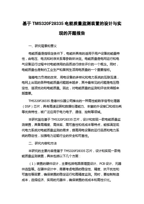
1.伺服驱动器结构及原理伺服驱动器主要由DSP(TMS320F28335)、主电路、驱动模块、检测模块、通信模块和人机接口模块等部分组成,如图1所示。
图1 伺服驱动器原理框图伺服驱动器通过光电编码器和电流传感器将电机的转速,方向和电流信号送给DSP处理器,将给定的信号与采集的信号进行比较,经过PID控制算法后输出SPWM波形,使电机达到所设定值。
2.硬件系统设计2.1 DSP控制器TMS320F28335芯片主频150MHz,具有32位浮点运算能力,6个DMA通道,支持ADC,McBSP,ePWM,XINTF 和SARAM,片内有256K×16大小的FLASH程序存储器和34K×16大小的SARAM,具有18路的PWM输出,采用1.8V内核电压,3.3V外围接口电压供电。
2.2 主电路及驱动电路2.2.1 电源模块TMS320F28335工作电源为 3.3V和 1.9V/1.8V。
所以采用了TI公司的TPS767D318芯片给DSP供电。
该芯片是TI公司专为DSP供电所设计,输入电压为5V,能同时产生3.3V和1.8V两种电压,而且该芯片自带电源监控和复位功能。
基于TMS320F28335电能质量监测装置的设计与实现的开题报告一、研究背景和意义电能质量是指给定条件下,电能所具有的适用于用户设备的能量特性,由电压、电流和时序关系等参数所决定。
电能质量是电网运行和电气设备运行过程中对电能使用的品质进行综合评价的一个概念。
同时,电能质量也是制约工业生产和居民生活用电质量的一个重要指标。
随着电力负荷的改变、用电设备的多样化和电力系统的互联互通,电网上出现的各种电能质量问题越来越多,其中最常见的问题是电压稳定性、谐波扰动和电能质量。
因此,对电能质量的监测和评估变得越来越重要。
TMS320F28335是德州仪器公司推出的一种高性能数字信号处理器(DSP)芯片,具有高速运算和数据处理能力、丰富的外设接口和低功耗等优良特性,被广泛应用于电力电子、通信、控制等领域。
本研究旨在基于TMS320F28335芯片,设计和实现一款电能质量监测装置,具备高精度、高效率、高可靠性和低成本等特点,能够满足现代电力系统对电能质量监测的需求,提高用电设备的运行品质和电力系统的稳定性,加强电力运输行业的安全和可靠性。
二、研究内容和方法本研究的主要内容是基于TMS320F28335芯片,设计和实现一款电能质量监测装置,具体包括以下几个方面:(1)装置的硬件设计,主要包括电路原理图设计、PCB设计、元器件选型等。
在硬件设计中,需要考虑电路的稳定性、精度、抗干扰性和可靠性等因素,确保装置的稳定运行和高精度监测。
同时,要控制制造成本,选择经济、实用的元器件,确保装置的低成本和高性价比。
(2)装置的软件设计,主要包括嵌入式软件设计、上位机软件设计等。
在软件设计中,需要考虑实时性、高效率、可靠性等因素,保证装置的快速响应和高效监测。
同时,要充分利用TMS320F28335芯片的优良特性,如高速运算、丰富的外设接口等,优化软件设计,提高装置的整体性能。
(3)装置的实验验证,主要包括功能测试、性能测试和实际应用测试。
基于TMS320F28335的永磁同步电机伺服系统设计与实现的开题报告一、选题的背景和意义永磁同步电机具有高效率、高功率密度、响应快等优点,被广泛应用于工业、家电、交通等领域。
而永磁同步电机的精准控制则需要使用高性能的数字信号处理器和专业的控制算法。
本课题选用TMS320F28335数字信号处理器为处理核心,设计并实现一个永磁同步电机伺服系统,通过PID控制算法对永磁同步电机进行转速、电流控制,并验证控制效果,为永磁同步电机的应用提供有效的控制手段。
二、研究内容和方法1.系统硬件设计:设计基于TMS320F28335的永磁同步电机伺服系统的硬件电路,包括主控板、驱动板、电源等模块设计。
2.系统软件设计:采用C语言编程,配置DSP芯片的引脚、计时器、ADC、PWM等外设,编写PID控制算法对永磁同步电机进行控制。
3.系统测试:通过测试,验证系统的控制效果和稳定性,调整控制参数,优化控制算法。
三、预期结果通过本课题的设计和实现,达到以下预期目标:1.设计出基于TMS320F28335的永磁同步电机伺服系统硬件电路图和PCB布图。
2.成功实现TMS320F28335控制永磁同步电机的控制程序,实现永磁同步电机转速、电流的稳定控制。
3.验证控制效果和稳定性,评估控制算法的优劣,并调整参数,优化算法。
四、研究难点和解决方案1.永磁同步电机的控制算法研究:针对永磁同步电机在转速控制、电流控制等方面的特点,学习和研究PID控制算法和其他控制算法,根据系统实际情况选择合适的控制算法。
2.硬件电路设计:参考TMS320F28335的数据手册和千印网提供的设计资料,结合永磁同步电机驱动板的设计,绘制符合系统需求的电路图和PCB布图。
3.软件编程:掌握TMS320F28335的编程方法和程序设计,编写符合控制算法的程序,配置芯片的计时器、ADC、PWM等外设,实现对永磁同步电机的控制。
五、可行性分析1.技术可行性:TMS320F28335作为一款高性能数字信号处理器,具有强大的计算和处理能力,可以满足永磁同步电机的高精度控制需求。
Design of TMS320F28335 Based Simulation System of Fire-FightingEquipments Manual-Control-PadHao Fu 1, a *, Yixin Su 2, bSchool of Automation, Wuhan University of Technology, Wuhan, Hubei, 430000, Chinaa ****************,b ****************Keywords: TMS320F28335, fire-fighting equipments, manual-control-pad, W5300Abstract: In order to train the workers of power stations, a simulation system of the fire-fighting equipments manual-control-pad is designed with a high-performance 32-bit CPU TMS320F28335 and an Ethernet chip W5300. The simulation system will start or stop 8 virtual fire fighting equipments by operating the manual- control-pad, so as to simulate the actual fire alarm system. In this system, start signal or stop signal is sent to the upper computer through the Ethernet to start or stop the virtual fire-fighting equipments in it. This article elaborates the overall structure and working principles of the simulation system and puts some emphasis on the hardware principles as well as the software design strategies of the W5300 Ethernet interface. It also explains the flow chat of the software program. Practice indicates that this simulation system is able to work steadily and reliably.IntroductionPotential risks exist in places like power stations whose internal structure is complex, it ’s high time that we insured its safe and reliable operation. Once fire occurs in power station, the consequence it might bring is serious. Therefore, strict requirements for the operators ’ field operation are put forward and there is no room for error. The operators at post should receive high-level education and training, have superior safety consciousness and conditioned reflex to the fire alarm. For these reasons, a fire alarm simulation training system seems to be of great significance [1]. The fire-fighting equipment manual-control-pad simulation system is a main part of the fire alarm simulation training system. When the operators receive fire alarm signals or trouble signals, they are able to start or stop 8 fire fighting equipments (fume extractors, fire pumps, etc.) quickly and abate fire or troubles.Fire-fighting equipment manual-control-pad simulation system is consistent with the actual control pad in aspects of operation interface and function which makes it convenient for instructors to train the operator ’ skills and inculcate enough safety awareness in them. Apparently, this simulation system has practical implications.System Structure and Main FunctionA. System Structure. The fire-fighting equipments manual-control-pad simulation system is mainly consisted of the following parts: TMS320F28335, the W5300 Ethernet interface, the LED module, the keyboardFig.1 System structure figure of the fire-fighting equipments manual-control-pad simulation system.A high-performance 32-bit CPU TMS320F28335 is selected as the main control chip. The CPU, whose clock frequency reaches up to 150MHz, has many advantages such as fast processing rate, high precision, high performance, high peripheral integration, low cost, low power, large memory and fast 5th International Conference on Advanced Engineering Materials and Technology (AEMT 2015)response to interrupt. TMS320F28335 and W5300 share the sequential waveforms of CS signals, R/W signals, data bus and address bus, so it’s achievable for TMS320F28335 to connect and communicate with the position machine through the W5300 Ethernet interface. When the fire alarm signal occurs and the time is limited, TMS320F28335’s advantage of fast response to interrupt stands out [2].B.Main Function.When the operator receives fire alarm signals or trouble signals of a specific spot, he is supposed to start the corresponding fire fighting equipments or solve the trouble through the manual control pad. The manual control pad is consisted of 16 keys and 24 LEDs which are divided into 8 groups, it’s to say, every 2 keys and 3 LEDs are in a peer group. 8 groups are used to control 8 fire-fighting equipments. The manual control pad is connected to the upper computer by the cable. When the operator press the start key of a certain group, the corresponding start LED and running LED are turned on, and dynamic diagrams of the fire fighting equipments at the corresponding spot are shown in the upper computer’s interface. If the upper computer sends trouble signals to the manual control pad, the corresponding trouble LED is turned on. In this case, the operator should find and eliminate the troubles in time.Design of System HardwareA.Design of W5300 Ethernet Interface.W5300 is a chip with integration of 10/100M Ethernet Controller, MAC and TCP/IP protocol stack. It’s convenient, steady, and is widely used in the high-performance, low cost embedded fields. W5300 is easy to be connected with the CPU by the Bus Interface in direct access mode or indirect access mode. The load of CPU decreases for the reason of W5300’s ability to process communication protocol in it, therefore, the performance of CPU improves significantly. The schematic diagram of the hardware interface betweenW5300 and TMS320F28335 is shown in Fig2.Fig.2 The schematic diagram of the hardware interface betweenW5300 and TMS320F28335.In the design, W5300’s TEST_MODE [3:0] pins and OP_MODE [2:0] pins are grounded to set it as the internal PHY mode (normal running mode). Connect its address bus, data bus, the CS pin, the R/W pin, the interrupt pin and the reset pin with the corresponding pins of TMS320F28335. Connect the differential input signals RXIP, RXIN and the differential output signals TXOP, TXON with the HR911105A cable interface. With the addition of power and ground, the hardware interface of W5300 is available [3].B.Design of Keys and LEDs Modules24 LEDs are divided into three groups. With the addition of current-limiting resistances, 8 LEDs with common anode in each group are connected to the GIOPs of TMS320F28335 through a bi-directional tri-state data buffer. 74HC245 is an eight-channel tri-state data buffer with controlled direction. Its main function is to realize the two-way asynchronous communication of the data bus. Data buffer is often applied to protect the fragile main control chip.16 keys are connected between the power and ground through current-limiting resistances.Design of System SoftwareA.Design of Main ProgramSystem software includes W5300 Ethernet Interface program and key-LED interrupt program. The main program achieves the following function: the initialization of variables, DSP’s peripheral and W5300, etc. The initialization of variables mainly defines some flag bits to make it convenient to execute, read and modify the programs. The initialization of DSP’s peripheral open or shield some function of DSP to ensure the execution of the following program and the initialization of W5300 is the basis of Ethernet connection. The flow chart of the main program is shown in Fig.3 (a).(b)Fig.3 Flow chart of the main program and the key-LED interrupt programB.Design of W5300 Ethernet Interface Program.The initialization of W5300 includes three steps: the host settings, network information settings and the allocation of TX/RX storage. During initialization, W5300 is set as direct address mode with 16-bit bus width. The data bus exchange and FIFO exchange are prohibited. Enable the interrupt of socket0 and disable the rest. Then we set the gateway address of local CPU as”192.168.0.254”, set the subnet mask as”255.255.255.0”, set the IP address as”192.168.0.1”. When data bags are failed to be sent, W5300 will repeat the sending process at a time interval of 200ms, for 8 times. Finally, TX/RX storage is allocated and the size of TX/RX of socket0 is defined. After the steps above-mentioned, the initialization is completed.After the initialization, W5300 is supposed to open sockets and exchange data via TCP. TCP is a kind of communication protocol. In TCP mode, we should firstly establish the connection to the end port according to the IP and socket number. In this way, date could be sent or received via the socket. When we establish a socket connection, “TCP server mode” or “TCP client mode” can be chosen. “TCP server”awaits connection request from the end port passively while “TCP client”asks for connection actively. In this design, the manual control pad is set as “TCP server mode” and awaits the connection request from the upper computer.As is shown in Fig.3, after setting W5300 as “TCP server mode”, several judgments are followed: connect or not, receive data or not, send data or not, receive FIN (end signal) or not, disconnect or not, timeout or not. If there is data to be sent or received, the process of sending or receiving data will be executed. The connection will be maintained until FIN is received or the socket is disconnected [4].C.Design of Key-LED Interrupt ProgramThe key and LED program is designed with timer interrupt. When the program enters the interrupt, key-vibration is eliminated. Then judge whether the key is pressed or not. If the start key is pressed, the start LED will be on and start signal will be sent to the upper computer; if the stop key is pressed, thestart LED and running LED will be off and stop signal will be sent to the upper computer. Finally, the program returns from interrupt. The flow chart of key-LED interrupt program is shown as Fig.3(b).The Experimental ResultAfter setting the IP of the upper computer and connecting to the Ethernet with a cable, tests can be started. Firstly click the “connect” button in the upper computer, when “connect to server” appeared in the log, connection is established. Under normal condition, if the start key of the fume extractor in “room one” is pressed, the start, running LEDs will be on and a dynamic graph of the fume extractor will be vividly shown in the upper computer, as is shown in Fig.4(a), Fig.5(a). Click the picture of fume extractor and a “red cross” appears, this indicates the trouble condition. This time when the start key is pressed, the red start LED and yellow trouble LED is on but the fume extractor fails to work, as is shown in Fig .4(b), Fig.5(b). The simulating control of the other equipments is analogous.(a) (b)Fig.4 upper computer and manual control pad under normal condition(a) (b)Fig.5 upper computer and manual control pad under trouble condition ConclusionThe simulation system of the fire-fighting equipment manual-control-pad use TMS320F28335 as CPU. Its high-speed data processing ability ensures the timeliness of sending and receiving data. High-performance Ethernet chip W5300 with integration of TCP protocol decreases the load of CPU, so the performance of the CPU increases significantly. The result of the test indicates that the simulation system achieves the ideal function and works steadily. It is feasible to use it as the simulation training system in power stations.References[1] Pingsheng Xu. Simulator Training and Licensing Examination for Nuclear Power Station Operator [J].Nuclear Power Engineering, 2007, 28(4):108-111,121.[2]Texas Instruments.TMS320F28335, TMS320F28334, TMS320-F28332 Data Sheet / /sc/techlit. 2007.[3] Quanmei Ou. The design and realization of embedded Ethernet. Computer Knowledge and Technology, 2007(6):35-37[4] WIZnet Device,Inc.High-performance internet connectivity solution-W5300[EB/OL].(2008). http://www.wiznet.cokr.。
基于TMS320F28335的稳定平台伺服系统的设计研究高伟松;王立玲;肖金壮;王洪瑞【摘要】In order to realize high precision control of stable platform, its servo system is designed. This paper presents a servo control scheme based on TMS320F2833 DSP, and it shows hardware and software design of control system. The eQEP module of DSP and the photoelectric encoder are used to realize angle and speed measurement. Compared with the previous technology, this method greatly improved the real time and reliability of the system. Practice indicates that this method has the virtue of high detecting precision, easily programming and compact hardware.%为了实现稳定平台的高精度控制,设计了相应的伺服系统。
提出了一种基于TMS320F28335DSP的伺服控制方案,并给出了控制系统的硬件和软件设计。
采用DSP的eQEP模块和光电编码器来实现转角和转速测量。
与以往技术相比,该方法大大提高了系统的可靠性和实时性。
实验表明,该系统具有检测精度高、易于编程和硬件紧凑的特点。
【期刊名称】《微型机与应用》【年(卷),期】2012(031)009【总页数】3页(P29-31)【关键词】伺服;TMS320F28335;eQEP模块;光电编码器【作者】高伟松;王立玲;肖金壮;王洪瑞【作者单位】河北大学电子信息工程学院,河北保定071000;河北大学电子信息工程学院,河北保定071000;河北大学电子信息工程学院,河北保定071000;河北大学电子信息工程学院,河北保定071000【正文语种】中文【中图分类】TP29在伺服电机和伺服驱动器组成的高性能稳定平台伺服系统中,需要实时地获得伺服电机的转角和转速信息,高速高精度的传感器以及相应的外围电路设计是必不可少的。
收稿日期:2009-06-03作者简介:刘明(1973—),男,云南会泽人,高级工程师,博士研究生,主要研究领域为水下航行器组合导航。
基于T MS320F28335的小型导航计算机系统设计刘 明(西北工业大学航海学院,陕西西安 710072)摘要:设计了一种基于新型浮点DSP ———T MS320F28335的小型导航计算机取代以往基于双处理器结构的同类系统,完成6路模拟量和3路数字量实时采集的同时,实现低成本大容量的非易失数据存储,其浮点运算能力满足导航算法需求,双CAN 总线接口可接驳多种上位机,通过片内高速数据交换通道还可扩展高性能DSP 阵列。
跑车试验表明,该设计用更小的体积和功耗实现了低成本导航计算机系统。
关键词:惯性导航系统;导航计算机;数字信号处理器中图分类号:U666.125 文献标识码:A 文章编号:1000-8829(2009)12-0036-04D esi gn of M i n i a ture Nav i ga ti on Co m puter Syste m Ba sed on T M S 320F 28335L I U M ing(School of Marine Engineering,North western Polytechnical University,Xi ’an 710072,China )Abstract:An m iniature navigati on computer syste m based on ne w type fl oating 2point DSP ———T MS320F28335is designed t o rep lace si m ilar syste m on dual 2p r ocess ors .Six channels of anal og signal and three channels of digital signal are real 2ti m e sa mp led and saved in a l ow 2cost nonvolatile large me mory .The computing capability of fl oating 2point unit can satisfy perfor mance require ments of navigati on algorithm.Dual CAN can be shared with several kinds of upper computer .DSP array is constructed by on 2chi p high s peed interface .Gr ound vehicle test indicates that a l ower cost navigati on computer syste m with s maller volume and po wer consump ti on is real 2ized .Key words:I N S;navigati on computer;DSP 近几年来,基于GPS 、ME MS -I M U 、磁通门罗盘、里程计等传感器的小型车载组合导航系统备受关注,设计这一类系统所面临的挑战是如何在给定的导航精度下不断降低成本、体积和功耗。
基于TMS320F28335的伺服驱动器的设计【摘要】本文设计了一种基于DSP的交流伺服电机驱动器的组成和总体设计方案。
该驱动器采用TMS320F28335为核心控制电路,设计完成了驱动电路和人机交互界面电路,同时完成了软件程序设计。
【关键词】DSP;伺服驱动器;TMS320F28335引言伺服驱动系统是机电一体化技术的重要组成部分,随着现代工业的快速发展,交流伺服系统逐渐成为工业伺服系统的主流,在数控机床、工业控制等自动化装备中得到广泛的应用。
本文介绍了一种基于TMS320F28335的伺服驱动器设计方案。
TMS320F28335是TI公司设计的一款数字信号处理器,其主要面向工业控制领域,特别适用于电机控制、运动控制等应用。
1.伺服驱动器结构及原理伺服驱动器主要由DSP(TMS320F28335)、主电路、驱动模块、检测模块、通信模块和人机接口模块等部分组成,如图1所示。
图1 伺服驱动器原理框图伺服驱动器通过光电编码器和电流传感器将电机的转速,方向和电流信号送给DSP处理器,将给定的信号与采集的信号进行比较,经过PID控制算法后输出SPWM波形,使电机达到所设定值。
2.硬件系统设计2.1 DSP控制器TMS320F28335芯片主频150MHz,具有32位浮点运算能力,6个DMA通道,支持ADC,McBSP,ePWM,XINTF 和SARAM,片内有256K×16大小的FLASH程序存储器和34K×16大小的SARAM,具有18路的PWM输出,采用1.8V内核电压,3.3V外围接口电压供电。
2.2 主电路及驱动电路2.2.1 电源模块TMS320F28335工作电源为 3.3V和 1.9V/1.8V。
所以采用了TI公司的TPS767D318芯片给DSP供电。
该芯片是TI公司专为DSP供电所设计,输入电压为5V,能同时产生3.3V和1.8V两种电压,而且该芯片自带电源监控和复位功能。
基于TMS320F28335的雷达伺服系统的设计与实现李红卫,刘昊,李勇臻(中国电子科技集团公司第二十七研究所,河南郑州450047)摘要:以TMS320F28335为核心,设计了一种高可靠性的雷达伺服系统。
描述了伺服系统的组成及其工作原理,重点讨论了伺服控制器的设计,分析系统的安全控制策略,并给出具体实现的控制电路。
实践表明:系统具备精度高、稳定性好、可靠性高、易调试等特点。
关键词:伺服系统;控制器;TMS320F28335;安全控制策略中图分类号:TP271文献标识码:A文章编号:1674-6236(2013)01-0170-03Design and implementation of a radar servo system based on TMS320F28335LI Hong -wei ,LIU Hao ,LI Yong -zhen(The 27th Research Institute ,CETC ,Zhengzhou 450047,China )Abstract:It takes the chip TMS320F28335as the core to design a high -reliability radar servo system.The principle and structure of the servo system are described ,The design of the servo controller is mainly discussed ,The safety control strategy is analyed and the detail circuit diagram of which is given out.The result indicates the system has excellent characteristics in terms of precision ,stability ,reliability ,and it ’s easy to adjust.Key words:servo system ;controller ;TMS320F28335;safety control strategy收稿日期:2012-09-21稿件编号:201209155作者简介:李红卫(1978—),男,河南焦作人,工程师。
研究方向:自动控制。
伺服系统是雷达的重要组成部分,其性能的好坏直接影响雷达的动态性能和测量精度,如何保证其高精度、安全、可靠工作是雷达伺服系统设计的关键,本文介绍了一种基于TMS320F28335的雷达伺服系统的工程设计与实现的方法。
TMS320F28335是TI 公司最新推出的控制专用32位浮点DSP 芯片,它的机器周期最短只有约6ns ,芯片内部集成了丰富的外设资源,具有很强的信号处理及控制能力,在电机控制应用方面具有独到的优势。
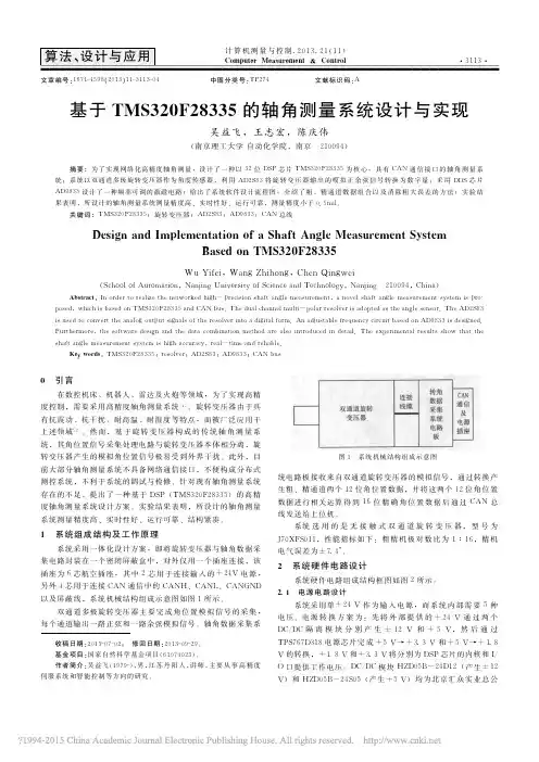
1系统组成及工作原理该雷达伺服系统主要由控制器、驱动器、电机、编码器、减速机构、电源及控保电路等部分组成,系统组成框图如图1所示[1-2]。
其工作原理为伺服控制器接收到控制命令后,进入相应的工作模式,经过控制运算后输出控制电压到伺服驱动器,驱动伺服电机带动转台按要求转动。
伺服系统环路设计采用电流环、速度换、位置环三环控制方案。
伺服控制器完成位置环闭环功能,伺服驱动器完成电流环和速度环的闭环功能。
电流环和速度环为位置环的内环,电流环设计为比例控制,速度环设计为比例积分控制,把设计好的电流环作为速度环的一个环节来设计。
为了保证系统精度,位置环设计为Ⅱ型系统,采用滑模变结构控制策略,以满足系统的稳定性和精度要求。
系统环路原理框图如图2所示。
伺服电机选用交流伺服电机,交流伺服电机因体积小、转动惯量小、过载能力强、控制简单等特点,在高精度、高可靠性的伺服驱动领域应用广泛[3]。
电机与转台方位轴和俯仰轴之间安装减速器。
系统位置检测采用光电编码器,根据系统精度的要求,采用16位的光电编码器,其测角分辨率为360216=0.00549°。
光电编码器通过联轴器安装于方位和俯仰电子设计工程Electronic Design Engineering第21卷Vol.21第1期No.12013年1月Jan.2013图2系统环路框图Fig.2System loop diagram图1系统组成框图Fig.1Composion block diagram of system-170-轴上。
驱动部分采用全数字交流伺服驱动器,速度控制模式,伺服驱动器内部运动控制参数可在线调整,方便调试。
2伺服控制器设计伺服控制器以TMS320F28335为控制核心,加上一些必要的外围电路构成。
伺服控制器的功能是实现位置闭环控制、串口通信、信号检测、故障检测及安全保护等功能。
2.1伺服控制器硬件组成伺服控制器硬件电路主要由DSP 主控芯片、DSP 外围电路、电源电路、D/A 转换电路、故障检测电路、电平转换电路、安全保护电路等构成[4-5],如图3所示。
系统外扩了512k ×16位SRAM ,方便系统调试时的外部仿真;采用AD7836外扩4路D/A 输出信号,其中两路作为正向通道,两路作为位前馈通道,经过控制运算后作为驱动器速度环路的输入信号;利用TMS320F28335芯片自带的3路SCI ,经接口芯片MAX3491电平转换后,将TTL 电平信号转换为RS422电平信号,实现伺服控制器与两路编码器及上位机的通信,所有输入输出的I/O 信号均通过光耦与外部隔离,起到保护DSP 内核的作用。
2.2D/A 转换电路设计系统要求的转速范围为0.05°/s ~60°/s ,则系统调速比600.05=1200,选用14位D/A 转换芯片AD7836(最高位为符号位),理论上其可输出的调速比为213=8192,可满足系统调速范围要求,该芯片可输出为4路14位模拟电压,电压建立时间10μs ,输出电压范围为±10V ,可方便与伺服驱动器连接。
D/A 转换电路如图4所示。
2.3系统控制软件设计系统软件在CCS3.3开发环境下用C 语言编写,采用模块化方法设计,便于调试,系统软件流程如图5所示。
其工作过程为:系统复位后首先对DSP 进行初始化,然后系统自检,如果自检异常,系统进入保护模式,切断伺服驱动器的SRV-ON 信号。
如果自检正常,则系统根据上位机指令进入相应的工作模式,进行数据采集、信号处理及串口通信,最后,伺服控制器判断是否系统有故障,如果无故障,则系统进入下一个循环周期,否则,系统进入保护模式,切断伺服驱动器的SRV-ON 信号。
2.4位置环路控制策略位置环设计是系统设计的关键环节,由于系统需要,该环路不能有振荡、超调现象,同时又要保证快速性。
在位置环的设计中采用了滑模变结构的控制方法,滑模控制的优点是能够克服系统的不确定性,对干扰和未建模动态具有很强的鲁棒性,尤其是对非线性系统的控制具有良好的效果。
其最大的优点是滑动模态对加在系统上的干扰和系统的摄动具有完全的自适应性,而且系统状态一旦进滑模运动,便能够快速收敛到目标控制,为时滞系统,不确定性系统的鲁棒性设计提供了一种有效的途径。
变结构控制可以解决系统大角速度调转和稳定过渡的难题;当位置误差小于一定量时,系统切换到PI 控制器,以此满足系统的稳定性和精度要求。
系统原理结构如图4所示,其中VSS 表示滑模变结构控制器,P+I 表示比例积分控制器[6-7]。
图6滑模变结构控制器原理Fig.6Principle of sliding mode variable structure controller图5系统软件流程图Fig.5Flow chart of system software图4D/A 转换电路Fig.4D/A conversion circuit图3控制器硬件组成Fig.3Hardware structure diagram ofcontroller李红卫,等基于TMS320F28335的雷达伺服系统的设计与实现-171-控制策略为:u =u 1=a 1x 1x 1s >0a 2x 1x 1s <0!,|ε|>Δθu 2=[P +I ],|ε|<Δ!θ2.5安全控制策略雷达伺服系统是一个复杂的机电一体化系统,在工作过程中处于高速转动状态,在人员操作失误或设备失控飞车的情况下,都有可能对人员或设备造成伤害,所以在系统设计时需要重点考虑安全控制策略,本系统的安全设计主要从以下几个方面入手:伺服驱动器上电延时设计、开机自检、DSP 自身工作检测、伺服驱动器检测、俯仰机构抱闸设计、通信链路检测、俯仰机构限位检测等。
安全控制逻辑组合电路如图7所示,其工作过程为:系统上电后,硬件延时电路对DELAY 信号进行延时,延时时间到之后,DELAY 输出高电平,延时的目的是为了保证各外围电路正常工作之后才能启动SRV-ON 信号。
DSP 自检完成之后,如果DSP 工作正常,则GPIO20送出方波信号,通过54HCT123将其展宽后变为高电平信号送入四2输入与门电路CD4081,否则54HCT123送出低电平信号,其作用是实时判断DSP 是否工作正常,防止程序跑飞或DSP 死机;TOP ,BOTTOM 为俯仰机构上、下限位信号,正常情况下为高电平,如果触发电气限位,则变为低电平;ALM 信号为DSP 送出的报警信号,如果DSP 检测到各故障报警信号均正常,则DSP 送出高电平,否则送出低电平。
CD4081对各路输入信号进行逻辑与运算,如果各检测信号均为高电平,则说明系统工作正常,启动SRV-ON ,伺服驱动器工作,否则认为伺服系统出现故障,SRV-ON 信号送出高电平,伺服驱动器停止工作。
3电磁兼容设计雷达系统是集微波、电子、电气、精密机械为一体的复杂装置。
其工作时将会产生各种感应和干扰,在这种复杂的电磁环境下工作,有可能导致伺服系统出现故障甚至无法正常运行;而伺服系统工作时本身也是一个干扰源,伺服驱动器内的电力电子器件的电流通断造成的开关噪声,电感负载电流切断引起的噪声,接通负载时的冲击电流和开关的抖动,动力传输线的发射,伺服控制器内高速数字电路运行产生的干扰等,这些干扰都有可能影响雷达系统其他设备的正常工作,因此伺服系统的电磁兼容设计不容忽视。
本系统电磁兼容设计主要从以下几个方面考虑:1)信号线连接使用屏蔽线,伺服控制器和伺服驱动器采用金属外壳封装,对电磁干扰进行隔离屏蔽。
2)在电路板设计及电缆走线时考虑高低压隔离,强弱电隔离,模拟电路和数字电路分开,交、直流电源分开。
3)合理接地,采用一点接地的方法,将电机外壳、动力线屏蔽层、驱动器外壳金属接地。