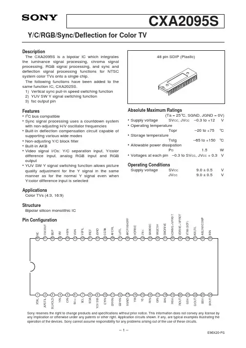
CXA2095SY/C/RGB/Sync/Deflection for Color TVDescriptionThe CXA2095S is a bipolar IC which integrates the luminance signal processing, chroma signal processing, RGB signal processing, and sync and deflection signal processing functions for NTSC system color TVs onto a single chip.The following functions have been added to the same function IC, CXA2025S.1) Vertical sync pull-in speed switching function 2)YUV SW Y signal switching function 3)fsc output pinFeatures•I 2C bus compatible•Sync signal processing uses a countdown system with non-adjusting H/V oscillator frequencies•Built-in deflection compensation circuit capable of supporting various wide modes •Non-adjusting Y/C block filter •Built-in AKB•Video signal I/Os: Y/C separation input, Y/color difference input, analog RGB input and RGB output•YUV SW Y signal switching function allows picture quality adjustment for the Y signal in the same manner as for the normal Y signal even when Y/color difference input is selected ApplicationsColor TVs (4:3, 16:9)StructureBipolar silicon monolithic ICPin ConfigurationAbsolute Maximum Ratings(Ta = 25°C, SGND, JGND = 0V)•Supply voltage SV CC , JV CC –0.3 to +12V •Operating temperatureTopr –20 to +75°C•Storage temperatureTstg –65 to +150°C•Allowable power dissipationP D 1.5W•Voltages at each pin –0.3 to SV CC , JV CC + 0.3V Operating Conditions Supply voltage SV CC9.0 ±0.5V JV CC9.0 ±0.5VSony reserves the right to change products and specifications without prior notice. This information does not convey any license by any implication or otherwise under any patents or other right. Application circuits shown, if any, are typical examples illustrating the operation of the devices. Sony cannot assume responsibility for any problems arising out of the use of these circuits.48 pin SDIP (Plastic)B L H O L DY I NX T A LA P C F I LC I NS V C CY U V S WE Y I NE R Y I NE B Y I NS G N DY MY SR I NG I NB I NR S HR O U TG S HG O U TB S HB O U TS C LS D AMK I N B L I N /V C O M P B L F I LCS C O U TS I NS I NS F I LR E FG N DG PE R AF C F I L2F I LF C P I N /H O F FD R I V EV C CA W O S CA G C S HW D R I V ED R I VE +/V P R O TD R I VE –/V P R O TT I M (S C P )S D AS C LB G PI R E FV S I NV S F I LH S I NN CA F C F I L J G N D C E R A L 2F I L A F C P I N /H O F F H D R I V E J V C C S A W O S C V A G C S H E W D R I V E V D R I V E +V D R I V E –/V P R O TV T I M A B L I N /V C O M PA B L F I L I K I NY I V B L H O L C I A P C F I X T A S V C Y U V S E Y I E R Y I E B Y I S G N Y Y R I G I B I R S G S B S B O U G O U R O U F S C O U B l o c k D i a g r a mPin DescriptionCXA2095SE l e c t r i c a l C h a r a c t e r i s t i c sS e t t i n g c o n d i t i o n s•T a = 25°C , S V C C = J V C C = 9V , S G N D = J G N D = 0V •M e a s u r e s t h e f o l l o w i n g a f t e r s e t t i n g t h e I 2C b u s r e g i s t e r a s s h o w n i n “I 2C b u s r e g i s t e r i n i t i a l s e t t i n g s ”.N o .I t e m S y m b o lM e a s u r e m e n t c o n d i t i o n sM e a s u r e -m e n t p i n M e a s u r e m e n t c o n t e n t s M i n .T y p .M a x .U n i t1S i g n a l b l o c k c u r r e n t c o n s u m p t i o nS I C CS V C C = 9.0V ,B u s d a t a = c e n t e r6M e a s u r e t h e p i n i n f l o w c u r r e n t .406590m A2S y n c b l o c k c u r r e n t c o n s u m p t i o nJ I C CJ V C C = 9.0V ,B u s d a t a = c e n t e r34M e a s u r e t h e p i n i n f l o w c u r r e n t .254560m AS y n c d e f l e c t i o n b l o c k i t e m s元器件交易网CXA2095SS i g n a l b l o c k i t e m s元器件交易网元器件交易网CXA2095S元器件交易网CXA2095SElectrical Characteristics Measurement Conditions “I2C bus register initial settings”PICTURE= 3F Hex C-TRAP= 0VM= 0HUE= 1F Hex DC-TRAN= 0D-PIC= 0COLOR= 1F Hex TOT= 0AXIS= 0BRIGHT= 1F Hex D-COL= 0ABL= 0SHARPNESS= 7 Hex PRE-OVER= 3SHP-F0= 2SUB-CONT= 7 Hex CTRAP-ADJ= 7 Hex SUB-COLOR= 7 Hex SUB-HUE= 7 Hex SUB-BRIGHT= 1F Hex GAMMA= 0G-DRIVE= 2A Hex AGING1= 0AGING2= 0B-DRIVE= 2A Hex G-CUTOFF= 0 Hex B-CUTOFF= 0 Hex EY-SW= 0CD-MODE2= 0RON= 1GON= 1BON= 1PICON= 1VOFF= 0FHHI= 0CD-MODE= 0AKBOFF= 0V-SIZE= 1F Hex V-COMP= 0V-POSITION= 1F Hex AFC-MODE= 1S-CORR= 0 Hex V-LIN= 7 Hex H-SIZE= 1F Hex REF-POSI= 3PIN-COMP= 1F Hex VBLKW= 0H-POSITION= 7 Hex PIN-PHASE= 7 Hex UP-CPIN= 0 Hex LO-CPIN= 0 Hex AFC-BOW= 7 Hex AFC-ANGLE= 7 Hex V-ASPECT= 0 Hex ZOOMSW= 0HBLKSW= 0V-SCROLL= 1F Hex JMPSW= 0UP-VLIN= 0 Hex LO-VLIN= 0 Hex LEFT-BLK= 7 Hex RIGHT-BLK= 7 HexA p p l i c a t i o n C i r c u i ti n p u t /o u t p u t s i g n a l i n p u t s i g n a l i n p u t R G B i n p u t Y s i g n a l i n p u tV p r o t e c t s i g n a l i n p u tl u c t u a t i o n a l i n p u tA p p l i c a t i o n c i r c u i t s s h o w n a r e t y p i c a l e x a m p l e s i l l u s t r a t i n g t h e o p e r a t i o n o f t h e d e v i c e s . S o n y c a n n o t a s s u m e r e s p o n s i b i l i t y f o r a n y p r o b l e m s a r i s i n g o u t o f t h e u s e o f t h e s e c i r c u i t s o r f o r a n y i n f r i n g e m e n t o f t h i r d p a r t y p a t e n t a n d o t h e r r i g h t d u e t o s a m e .CXA2095S Electrical Characteristics Measurement Circuitare all GND unless otherwise specified in the Measurement conditions column of ElectricalCharacteristics.ABL is 9V unless otherwise specified.33CTRAP-ADJ SUB-HUEB-CUTOFFV-LINPIN-PHASE LO-CPIN AFC-ANGLELO-VLIN RIGHT-BLKPICTURE HUE COLOR BRIGHTSUB-BRIGHT G-DRIVE B-DRIVEV-SIZE V-POSITIONH-SIZE PIN-COMPV-ASPECT V-SCROLLSHARPNESSSUB-CONT SUB-COLORG-CUTOFF S-CORRH-POSITION UP-CPIN AFC-BOWUP-VLIN LEFT-BLK Definition of I 2C Bus Registers Slave Addresses88H: Slave receiver 89H: Slave transmitterControl RegisterBIT0BIT1BIT2BIT3BIT4BIT5BIT6BIT7Sub Address ∗∗∗0 0 0 0 0 00 H ∗∗∗0 0 0 0 1 01 H ∗∗∗0 0 0 1 0 02 H ∗∗∗0 0 0 1 1 03 H ∗∗∗0 0 1 0 0 04 H ∗∗∗0 0 1 0 1 05 H ∗∗∗0 0 1 1 0 06 H ∗∗∗0 0 1 1 1 07 H ∗∗∗0 1 0 0 0 08 H ∗∗∗0 1 0 0 1 09 H ∗∗∗0 1 0 1 0 0A H ∗∗∗0 1 0 1 1 0B H ∗∗∗0 1 1 0 0 0C H ∗∗∗0 1 1 0 1 0D H ∗∗∗0 1 1 1 0 0E H ∗∗∗0 1 1 1 1 0F H ∗∗∗1 0 0 0 0 10 H ∗∗∗1 0 0 0 1 11 H ∗∗∗1 0 0 1 0 12 H ∗∗∗1 0 0 1 1 13 H ∗∗∗1 0 1 0 0 14 H ∗∗∗1 0 1 0 1 15 H ∗∗∗1 0 1 1 0 16 H ∗∗∗1 0 1 1 1 17 H C-TRAP DC-TRAN TOT D-COLVM D-PIC AXIS ABLPRE-OVERSHP-F0GAMMA AGING1EY-SWAGING2CD-MODE2AKBOFFCD-MODE FHHIVOFFPICONBONGONRONV-COMP AFC-MODEREF-POSI VBLKWZOOMSW JMPSW HBLKSW 0Status RegisterBIT00BIT11BIT20BIT3KILLERBIT4HNGBIT5VNGBIT6IKRBIT7HLOCKNote)EY-SW and CD-MODE2 have been added to the CXA2025S.∗: Don't careDescription of Registers<Control Register>Register name No. of bits FunctionPICTURE(6):Picture gain control (RGB gain control)0H = –15dB3FH = 0dB RGB output: 2.4Vp-p (I/O gain: +4.7dB, 1.4Vp-p input)C-TRAP(1):Y block chroma trap ON/OFF switch0 = Trap OFF1 = Trap ON (Y signal delay time adjusted when C-TRAP turned ON or OFF.)VM(1):Y signal differential output ON/OFF switch for VM0: Output OFF1: Output ON (2.0Vp-p)HUE(6):Hue control (Chroma demodulation axis control when SUB-HUE is 8H)0H = +35°Flesh color appears red.1FH = 0°3FH = –35°Flesh color appears green.DC-TRAN(1):Y DC transmission ratio selector switch0 = 100%1 = 82%DPIC(1):Y black expansion ON/OFF switch0 = OFF1 = ON Point of inflection: 30 IRECOLOR(6):Color gain control0H = Color OFF (–40dB or less)1FH = 0dB B output: 1.1Vp-p (I/O gain: +5.7dB, 0.57Vp-p input)3FH = +5.4dBTOT(1):Chroma TOT filter band selector switch0 = TOT-TRAP OFF1 = TOT-TRAP ON (TRAP f0 2.0MHz)AXIS(1):R-Y, G-Y axis selector switch0 = Japan axis R-Y: 95°×0.60, G-Y: 236°× 0.331 = US axis R-Y: 105°× 0.78, G-Y: 236°× 0.33(B-Y: 0°× 1)CXA2095SBRIGHT(6):Bright level control (RGB DC bias control)0H = –300mV1FH = 0mV–300mV from REF-P level3FH = +300mVD-COL(1):Dynamic color ON/OFF switch0 = Dynamic color OFF1 = Dynamic color ON (R, Bch level control)ABL(1):ABL mode selector switch0 = Picture ABL mode1 = Picture/bright ABL modeSHARPNESS(4):Sharpness gain control (Y aperture correction gain control)0H = –8dB7H = 1dBFH = +5.1dBPRE-OVER(2):Sharpness preshoot/overshoot ratio control0H = 1:1(PRE:OVER)3H = 5:1SHP-F0(2):Sharpness f0 control (Delay line current control for aperture correction)0H = 2.5MHz3H = 4.0MHzSUB-CONT(4):Contrast gain control (Y gain control)0H = –3.0dB7H = 0dBFH = +2.5dBCTRAP-ADJ(4):Chroma trap f0 adjustment (Y block chroma trap current control)0H = +300kHz7H = 0kHzFH = –300kHzfsc adjustable to –30dB or less (SHP-F0 min.); adjustment value: 3 to 4SUB-COLOR(4):Color gain control (ACC reference level control)0H = –4.0dB7H = 0dBFH = +2.1dBCXA2095SSUB-HUE(4):Hue control (Phase control for chroma demodulation axis when HUE = 1FH)0H = +10°7H = 0FH = –10°B-Y axis adjustable to 0°SUB-BRIGHT(6):Bright level control (RGB DC bias control)0H = –300mV1FH = 0mV–300mV from REF-P level3FH = +300mVGAMMA(2):Gamma control (RGB gamma correction amount control)0H = Gamma OFF3H = Gamma peak (40 IRE) +400mVG-DRIVE(6):Gch drive gain adjustment (Gch gain control)0H = G/R–3.8dB2AH = G/R0dB3FH = G/R+2.5dBAGING1(1):White output aging mode ON/OFF switch(Has priority over RGBON and PICON control, set to OFF mode at power-on.)0 = Aging mode OFF1 = Aging mode ON60 IRE flat signal output from Y block when input isno signalAGING2(1):Black output aging mode ON/OFF switch(Has priority over AGING1, set to OFF mode at power-on.)0 = Aging mode OFF1 = Aging mode ON Black level outputB-DRIVE(6):Bch drive gain adjustment (Bch gain control)0H = B/R–3.8dB2AH = B/R0dB3FH = B/R+2.5dBEY-SW(1):Internal Y signal fixed mode ON/OFF switch0 = YUV SW (Pin 9) standard operation (EYIN, ERYIN and EBYIN input areselected when Pin 9 is high.)1 = EYIN (Pin 10) input only invalid (Internal Y, ERYIN and EBYIN input areselected when Pin 9 is high.)CD-MODE2(1):Vertical sync pull-in speed switch0 = Standard (equivalent to CXA2025S)1 = High speedCXA2095SG-CUTOFF(4):Gch cut-off adjustment (Gch reference pulse value control of IKIN pin input)0H = 62%7H = 100%(G/R:Gch reference pulse amplitude when Rch referenceFH = 150%pulse amplitude of IKIN pin input is assumed 100%)B-CUTOFF(4):Bch cut-off adjustment (Bch reference pulse value control of IKIN pin input)0H = 62%7H = 100%(B/R:Bch reference pulse amplitude when Rch referenceFH = 150%pulse amplitude of IKIN pin input is assumed 100%)RON(1):ON/OFF switch for Rch video output without a reference pulse(Operates when PICON = 1, set to OFF mode at power-on.)0 = Rch video output OFF (Blanked status, reference pulse only output)1 = Rch video output ONGON(1):ON/OFF switch for Gch video output without a reference pulse(Operates when PICON = 1, set to OFF mode at power-on.)0 = Gch video output OFF (Blanked status, reference pulse only output)1 = Gch video output ONBON(1):ON/OFF switch for Bch video output without a reference pulse(Operates when PICON = 1, set to OFF mode at power-on.)0 = Bch video output OFF (Blanked status, reference pulse only output)1 = Bch video output ONPICON(1):ON/OFF switch for RGB output with a reference pulse (Set to OFF mode atpower-on.)0 = RGB output OFF (All blanked status)1 = RGB output ONVOFF(1):V sawtooth wave oscillation stop ON/OFF switch (Set to OFF mode atpower-on.)0 = Oscillation stop OFF (VDRIVE– and VDRIVE+: normal output)1 = Oscillation stop ON (VDRIVE– and VDRIVE+: DC output and DC valuevary according to V-POSITION.)FHHI(1):H oscillator frequency fixation ON/OFF switch (Set to ON mode at power-on.)0 = H oscillator frequency fixation OFF AFC normal mode1 = H oscillator frequency fixation ON Oscillator frequency fixed tomaximum value (16.252kHz).CD-MODE(1):V countdown system mode selector switch(Set to automatic selection mode during power-on.)0 = Non-standard signal mode, standard signal mode and no signal modeautomatically selected1 = Fixed to non-standard signal mode(V oscillator frequency is 55Hz during no signal mode (free run).)CXA2095S AKBOFF(1):AKB ON/OFF switch (Set to ON mode at power-on.)0 = AKB ON1 = AKB OFF IK clamp, IK S/H and reference pulse fixed to OFF.R, G and B cut-off adjustment at AKB OFF performed by voltageapplied to Pins 19 (RSH), 21 (GSH) and 23 (BSH), respectively.V-SIZE(6):Vertical amplitude adjustment (V sawtooth wave gain control)0H = –14%Vertical picture size decreases.1FH = 0%Amplitude: 1.15Vp-p, center DC : 3V (when V-ASPECT = 1FH)3FH = +14%Vertical picture size increases.V-COMP(2):Compensation amount setting for vertical high voltage fluctuation (V sawtoothwave gain control)0H = 0%V sawtooth wave amplitude compensation amount when 1V isapplied with respect to when 9V is applied of VCOMP (Pin 26)3H = –5%V sawtooth wave amplitude compensation amount when 1V isapplied with respect to when 9V is applied of VCOMP (Pin 26)V-POSITION(6):Vertical position adjustment (V sawtooth wave DC bias control)0H = –0.09V Picture position drops, VDRIVE+ output DC Down1FH = 0V Center DC: 3V2FH = +0.09V Picture position rises, VDRIVE+ output DC UpAFC MODE(2):AFC loop gain control (PLL between Hsync and Hvco)0H = H free run mode1H = Small gain2H = Medium gain3H = Large gainS-CORR(4):Vertical S correction amount adjustment (V sawtooth wave secondary componentgain control)0H = Secondary component amplitude by adding sawtooth wave is 0FH = Secondary component amplitude by adding sawtooth wave is MaximumV-LIN(4):Vertical linearity adjustment (Gain control for V sawtooth wave secondarycomponent)0H = 85% (Bottom/top of picture) Top of picture expanded; bottom of picturecompressed.7H = 100% (Bottom/top of picture)FH = 115% (Bottom/top of picture) Top of picture compressed; bottom ofpicture expanded.H-SIZE(6):Horizontal amplitude adjustment (V parabola wave DC bias control)0H = –0.5V Horizontal picture size decreases, EWDRIVE output DC Down.1FH = 0V Amplitude: 0.58Vp-p, center DC: 4V (when V-ASPECT = 2FH)3FH = +0.5V Horizontal picture size increases, EWDRIVE output DC UpREF-POSI(2):Reference pulse timing setting0H = (From VTIM rise) Rch: 22H, Gch: 23H, Bch: 24H1H = (From VTIM rise) Rch: 20H, Gch: 21H, Bch: 22H2H = (From VTIM rise) Rch: 18H, Gch: 19H, Bch: 20H3H = (From VTIM rise) Rch: 16H, Gch: 17H, Bch: 18HCXA2095S PIN-COMP(6):Horizontal pin distortion compensation amount adjustment (V parabola wavegain control)0H = 0.11Vp-p Compensation amount minimum1FH = 0.47Vp-p Center DC: 4V (when V-ASPECT = 2FH)3FH = 0.84Vp-p Compensation amount maximumVBLKW(2):VBLK width control (Blanked width after reference pulse. Operates whenJMPSW = 1, blanked width after reference pulse is fixed to 1H when JMPSW = 0.)0H = 12H from Bch REF-P1H = 11H from Bch REF-P2H = 10H from Bch REF-P3H = 9H from Bch REF-PH-POSITION(4):Horizontal position adjustment (HAFC phase control)0H = 1µs delay Picture position shifts to right. Video delayed withrespect to HD.7H = 0µsFH = 1µs advance Picture position shifts to left. Video advanced withrespect to HD.PIN-PHASE(4):Horizontal trapezoidal distortion compensation amount adjustment (V parabolawave center timing control)0H = 1.5ms advance Horizontal size for top of picture increases.Horizontal size for bottom of picture decreases.7H = 0ms Center timing is 8.9ms from VTIM.FH = 1.5ms delay Horizontal size for top of picture decreases.Horizontal size for bottom of picture increases.UP-CPIN(4):Horizontal pin distortion compensation amount adjustment for top of picture (Vparabola wave gain control)0H = +0.2V Horizontal size for top of picture decreases.7H = 0V(0.7Vp-p, 4:3 mode)FH = –0.2V Horizontal size for top of picture increases.LO-CPIN(4):Horizontal pin distortion compensation amount adjustment for bottom of picture(V parabola wave gain control)0H = +0.2V Horizontal size for bottom of picture decreases.7H = 0V(0.7Vp-p, 4:3 mode)FH = –0.2V Horizontal size for bottom of picture increases.AFC-BOW(4):Vertical line bow compensation amount adjustment (HAFC phase controlaccording to parabola wave)0H = Top and bottom of picture delayed 500ns with respect to picture center7H = 0nsFH = Top and bottom of picture advanced 500ns with respect to picture center AFC-ANGLE(4):Vertical line slope compensation amount adjustment (HAFC phase controlaccording to sawtooth wave)0H = Top of picture delayed 500ns, bottom of picture advanced 500ns withrespect to picture center7H = 0nsFH = Top of picture advanced 500ns, bottom of picture delayed 500ns withrespect to picture centerV-ASPECT(6):Aspect ratio control(V sawtooth wave gain control)0H = 75%16:9 CRT full2FH = 100%4:3 CRT full (amplitude: 1.23Vp-p)3FH = 112%CXA2095SZOOMSW(1):Zoom mode ON/OFF switch for 16:9 CRT(Top and bottom of V sawtooth wave squeezed and 25% of picture cut)0 = Zoom OFF Sawtooth wave amplitude: 1.23Vp-p1 = Zoom ON Sawtooth wave amplitude: 70%HBLKSW(1):HBLK width control ON/OFF switch during 4:3 software full display mode on a16:9 CRT0 = Control OFF HBLK pulse generated from HPIN.1 = Control ON HBLK pulse generated as pulse generated from HPIN or aspulse generated from HVCO and width adjusted.Width adjustment is performed by the LEFT-BLK and RIGHT-BLK registers.V-SCROLL(6):Vertical picture scroll control during zoom mode on a 16:9 CRT(DC component added to sawtooth wave AGC output to control ZOOMSW cuttiming)0H = –0.25V Scrolled toward top of screen by 32H and top of picturezoomed.1FH = 0V3FH = +0.25V Scrolled toward bottom of screen by 32H and bottom of picturezoomed.JUMPSW(1):Reference pulse jump mode ON/OFF switch(In addition to V-ASPECT control, sawtooth wave gain control performed for100% of VBLK interval and 67% of picture interval)0 = Jump mode OFF1 = Jump mode ONOn a 4:3 CRT, jump mode expands the sawtooth wave amplitude to 112%with V-ASPECT; on a 16:9 CRT, jump mode compresses the sawtoothwave amplitude to 75% with V-ASPECT. The V blanking width is expandedat both the top and bottom of the picture. Blanking for the bottom of thepicture starts 251H after VTIM, and blanking for the top of the picture canbe varied as the blanking width after the reference pulse by the VBLKWregister.UP-VLIN(4):Vertical linearity adjustment for top of picture(Secondary component gain control for sawtooth wave added to sawtooth waveAGC output)0H = 100% (Bottom/top of picture)FH = 115% (Bottom/top of picture) Top of picture compressed.LO-VLIN(4):Vertical linearity adjustment for bottom of picture(Tertiary component gain control for sawtooth wave added to sawtooth waveAGC output)0H = 100% (Bottom/top of picture)FH = 85% (Bottom/top of picture) Bottom of picture compressed.LEFT-BLK(4):HBLK width control for left side of picture when HBLKSW = 1(Phase control for timing pulse generated from HVCO)0H = +1.3µs HBLK width maximum7H = 0µs Center HBLK: 13µsFH = –1.3µs HBLK width minimumRIGHT-BLK(4):HBLK width control for the right side of picture when HBLKSW = 1(Phase control for timing pulse generated from HVCO)0H = +1.3µs HBLK width maximum7H = 0µs Center HBLK: 13µsFH = –1.3µs HBLK width minimum<Status Register>HLOCK(1):Lock status between Hsync and HVCO0 = HVCO free run status1 = Locked to HsyncIKR(1):AKB operation status0 = REF-P return small and AKB loop unstable.1 = REF-P return sufficient and AKB loop stable.VNG(1):Signal input status to VPROT pin0 = No VPROT input1 = VPROT input (In this case, RGB outputs are blanked.)HNG(1):Signal input status to HOFF pin0 = No HOFF input1 = HOFF input (In this case, RGB outputs are blanked.)KILLER(1):Color killer status0 = Killer OFF status1 = Killer ON statusNote)The following have been added to the CXA2025S.EY-SW: Sub Add 09H, Bit 1CD-MODE2: Sub Add 09H, Bit 0Description of Operation1. Power-on sequenceThe CXA2095S does not have an internal power-on sequence. Therefore, all IC operations are controlled by the set microcomputer (I2C bus controller).1) Power-onThe IC is reset and the RGB outputs are all blanked. Hdrive starts to oscillate, but oscillation is at the maximum frequency (16kHz or more) and is not synchronized to the input signal. Output of vertical signal VTIM starts, VDRIVE outputs V sawtooth wave. Bus registers which are set by power-on reset are as follows.AGING1= 0: All white output aging mode OFFAGING2= 0: All black output aging mode OFFRON= 0: Rch video blanking ONGON= 0: Gch video blanking ONBON= 0: Bch video blanking ONPICON= 0: RGB all blanking ONVOFF= 0: V sawtooth wave oscillation mode ∗VOFF = 1 for the CXA2025S.FHHI= 1: H oscillator maximum frequency modeCD-MODE= 0: Automatic selector mode of the countdown modeAKBOFF= 0: AKB mode2) Bus register data transferThe register setting sequence differs according to the set sequence. Register settings for the following sequence are shown as an example.Set sequence CXA2095S register settingsPower-on Reset status in 1) above.↓↓Degauss Reset status in 1) above.The CRT is degaussed in the completely darkened condition.↓↓IC initial setting The IC is set to the power-on initial settings. (See the following page.)The HDRIVE oscillator frequency goes to the standard frequency (around15.734kHz).↓↓AKB operation start PICON is set to 1 and a reference pulse is output from Rout, Gout andBout. Then, the IC waits for the cathode to warm up and the beam currentto start flowing.↓↓AKB loop stable Status register IKR is monitored.IKR = 0: No cathode currentIKR = 1: Cathode currentNote that the time until IKR returns to 1 differs according to the initialstatus of the cathode.↓↓Video output RON, GON and BON are set to 1 and the video signal is output fromRout, Gout and Bout.3) Power-on initial settingsThe initial settings listed here are reference values, and initial settings may be determined freely according to the set usage conditions.PICTURE= 3F Hex Max (User Cont.)C-TRAP= 0Chroma Trap OFFVM= 1VM out ONHUE= 1F Hex Center (User Cont.)DC-TRAN= 0Y DC transmission ratio 100%D-PIC= 1Y black expansion ONCOLOR= 1F Hex Center (User Cont.)TOT= 0Chroma low frequency increasedAXIS= 0R-Y, G-Y Japan axisBRIGHT= 1F Hex Center (User Cont.)D-COL= 1Dynamic Color ONABL= 1Picture/bright ABL modeSHARPNESS= 7 Hex Center (User Cont.)PRE-OVER= 0Sharpness pre/over ratio 2:1SHP-F0= 1Sharpness f0 3MHzSUB-CONT= 7 Hex Center (Adjust)CTRAP-ADJ= 7 Hex Center (Adjust)SUB-COLOR= 7 Hex Center (Adjust)SUB-HUE= 7 Hex Center (Adjust)SUB-BRIGHT= 1F Hex Center (Adjust)GAMMA= 0Gamma OFFG-DRIVE= 1F Hex Center (Adjust)AGING1= 0Aging Mode OFFAGING2= 0Aging Mode OFFB-DRIVE= 1F Hex Center (Adjust)G-CUTOFF= 7 Hex Center (Adjust)B-CUTOFF= 7 Hex Center (Adjust)EY-SW= 0StandardCD-MODE2= 0StandardRON= 0Rch video output OFFGON= 0Gch video output OFFBON= 0Bch video output OFFPICON= 0RGB all blankedVOFF= 0Vdrive oscillation stoppedFHHI= 0Horizontal oscillator frequency standardCD-MODE= 0V countdown auto modeAKBOFF= 0AKB ONV-SIZE= 1F Hex Center (Adjust)V-COMP= 3Vdrive high voltage fluctuation compensation amount maxV-POSITION= 1F Hex Center (Adjust)AFC-MODE= 2CenterS-CORR= 7 Hex Center (Adjust)V-LIN= 7 Hex Center (Adjust)H-SIZE= 1F Hex Center (Adjust)REF-POSI= 0PIN-COMP= 1F Hex Center (Adjust)VBLKW= 0(Power-on initial settings cont.)H-POSITION= 7 Hex Center (Adjust)PIN-PHASE= 7 Hex Center (Adjust)UP-CPIN= 7 Hex Center (Adjust)LO-CPIN= 7 Hex Center (Adjust)AFC-BOW= 7 Hex Center (Adjust)AFC-ANGLE= 7 Hex Center (Adjust)V-ASPECT= 0 Hex16:9 CRT Full ModeZOOMSW= 116:9 CRTHBLKSW= 1Hblk width adjust ONV-SCROLL= 1F Hex Center (User)JMPSW= 016:9 CRT Full ModeUP-VLIN= 7 Hex16:9 CRT Full ModeLO-VLIN= 7 Hex16:9 CRT Full ModeLEFT-BLK= F Hex Hblk width min.RIGHT-BLK= F Hex Hblk width min.2. Various mode settingsThe CXA2095S contains bus registers for deflection compensation which can be set for various wide modes. Wide mode setting registers can be used separately from registers for normal picture distortion adjustment, and once distortion adjustment has been performed in full mode, wide mode settings can be made simply by changing the corresponding register data.•VDRIVE signal picture distortion adjustment registersV-SIZE, V-POSITION, S-CORR, V-LIN•E/WDRIVE signal picture distortion adjustment registersH-SIZE, PIN-COMP, PIN-PHASE, UP-CPIN, LO-CPIN•Wide mode setting registersV-ASPECT, ZOOMSW, HBLKSW, V-SCROLL, JMPSW, UP-VLIN, LO-VLIN, LEFT-BLK, RIGHT-BLKExamples of various modes are listed below. These modes are described using 480 lines as the essential number of display scanning lines. Wide mode setting register data is also listed, but settings may differ slightly due to IC variation. The standard setting data differs for 16:9 CRTs and 4:3 CRTs.Register 16:9 CRT 4:3 CRTV-ASPECT0 H2F HV-SCROLL1F H1F HZOOMSW10UP-VLIN0 H0 HLO-VLIN0 H0 HJMPSW00HBLKSW00LEFT-BLK7 H7 HRIGHT-BLK7 H7 H1) 16:9 CRT full modeThis mode reproduces the full 480 lines on a 16:9 CRT. 4:3 images are reproduced by stretching the picture to the left and right. Normal images are compressed vertically, but 16:9 images can be reproduced in their original 16:9 aspect ratio with a video source which compresses (squeezes) 16:9 images to 4:3 images.The register settings are the 16:9 CRT standard values.2) 16:9 CRT normal modeIn this mode, 4:3 images are reproduced without modification. A black border appears at the left and right of the picture. In this mode, the H deflection size must be compressed by 25% compared to full mode. The CXA2095S also has a register (H-SIZE) which controls the H size, but the control width is not sufficient for 25% compression. Therefore, external measures must be taken such as switching the H deflection coil. Full mode should be used when performing memory processing and attaching a black border to the video signal.H blanking of the image normally uses the flyback pulse input to AFCPIN (Pin 36). However, the blanking width can be varied according to the control register setting when blanking is insufficient for the right and left black borders.The following three settings are added to the 16:9 CRT standard values for the register settings.HBLKSW = 1LEFT-BLK = Adjustment valueRIGHT-BLK = Adjustment valueThe H angle of deflection also decreases, causing it to differ from the PIN compensation amount during H size full status. Therefore, in addition to the wide mode registers, PIN-COMP must also be readjusted only for this mode.3) 16:9 CRT zoom modeIn this mode, 4:3 images are reproduced by enlarging the picture without other modification. The top and bottom of normal 4:3 images are lost, but almost the entire picture can be reproduced for vista size video software, etc. which already has black borders at the top and bottom. The enlargement ratio can be controlled by the V-ASPECT register, and enlarging the picture by 33% compared to full mode allows zooming to be performed for 4:3 images without distortion. In this case, the number of scanning lines is reduced to 360 lines compared to 480 lines for full mode. The zooming position can be shifted vertically by the V-SCROLL register. V blanking of the image normally begins from V sync and continues for 2H after the AKB reference pulse, and the top and bottom parts are also blanked during this mode.Adjust the following two registers with respect to the 16:9 CRT standard values for the register settings.V-ASPECT = 2FHV-SCROLL = 1FH or user control4) 16:9 CRT subtitle-in modeWhen Cinema Scope size images which have black borders at the top and bottom of the picture are merely enlarged with the zoom mode in 3) above, subtitles present in the black borders may be lost. Therefore, this mode is used to super-compress only the subtitle part and reproduce it on the display.Add the LO-VLIN adjustment to the zoom mode settings for the register settings.V-ASPECT = 2FHV-SCROLL = 1FH or user controlLO-VLIN = Adjustment valueThe LO-VLIN register causes only the linearity at the bottom of the picture to deteriorate. Therefore, UP-VLIN should also be adjusted if the top and bottom of the picture are to be made symmetrical. Since the picture is compressed vertically, the number of scanning lines exceeds 360 lines.。