
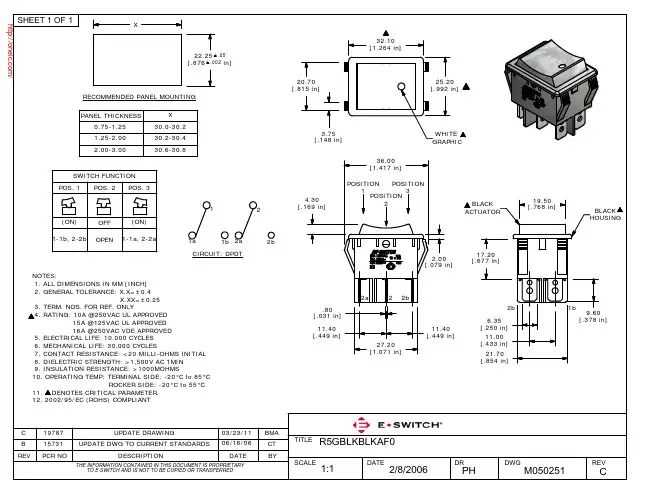
R5GBLKBLKAF0;中文规格书,Datasheet资料
- 格式:pdf
- 大小:116.88 KB
- 文档页数:2
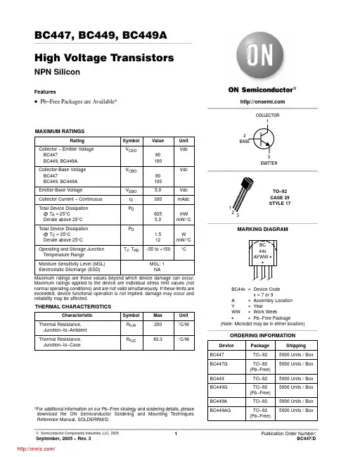

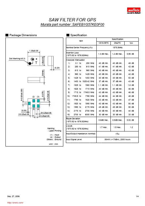
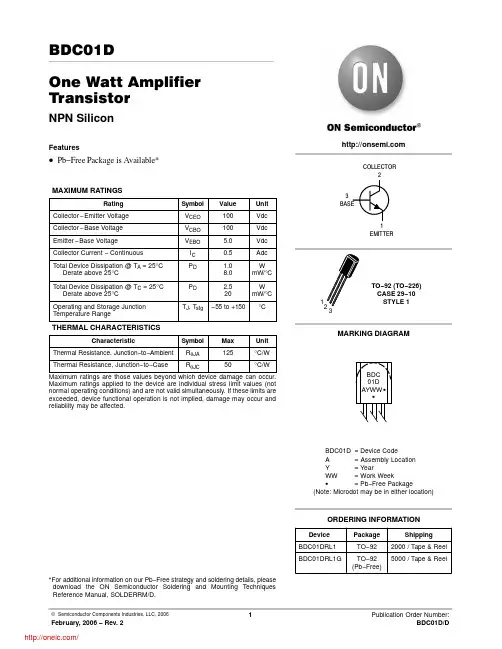
BDC01DOne Watt Amplifier TransistorNPN SiliconFeatures•Pb−Free Package is Available*MAXIMUM RATINGSRating Symbol Value Unit Collector−Emitter Voltage V CEO100Vdc Collector−Base Voltage V CBO100Vdc Emitter−Base Voltage V EBO 5.0Vdc Collector Current − Continuous I C0.5AdcTotal Device Dissipation @ T A = 25°C Derate above 25°C P D 1.08.0WmW/°CTotal Device Dissipation @ T C = 25°C Derate above 25°C PD 2.520WmW/°COperating and Storage JunctionTemperature RangeT J, T stg−55 to +150°C THERMAL CHARACTERISTICSCharacteristicSymbol Max Unit Thermal Resistance, Junction−to−Ambient R q JA125°C/W Thermal Resistance, Junction−to−Case R q JC50°C/W Maximum ratings are those values beyond which device damage can occur. Maximum ratings applied to the device are individual stress limit values (not normal operating conditions) and are not valid simultaneously. If these limits are exceeded, device functional operation is not implied, damage may occur and reliability may be affected.*For additional information on our Pb−Free strategy and soldering details, please download the ON Semiconductor Soldering and Mounting Techniques Reference Manual, SOLDERRM/D.Device Package ShippingORDERING INFORMATIONBDC01DRL1TO−922000 / Tape & ReelBDC01DRL1G TO−92(Pb−Free)5000 / Tape & ReelCOLLECTOR31EMITTERELECTRICAL CHARACTERISTICS (T A = 25°C unless otherwise noted)CharacteristicSymbolMinMaxUnitOFF CHARACTERISTICS Collector −Emitter Voltage(I C = 10 mA, I B = 0)V (BR)CEO 100−Vdc Collector Cutoff Current(V CB = 100 V, I E = 0)I CBO −0.1m Adc Emitter Cutoff Current(I C = 0, V EB = 5.0 V)I EBO−100nAdcON CHARACTERISTICSDC Current Gain(I C = 100 mA, V CE = 1.0 V)(I C = 500 mA, V CE = 2.0 V)h FE4025400−−Collector −Emitter Saturation Voltage (Note 1)(I C = 1000 mA, I B = 100 mA)V CE(sat)−0.7Vdc Collector −Emitter On Voltage (Note 1)(I C = 1000 mA, V CE = 1.0 V)V BE(on)−1.2VdcDYNAMIC CHARACTERISTICSCurrent Gain Bandwidth Product(I C = 200 mA, V CE = 5.0 V, f = 20 MHz)f T 50−MHz Output Capacitance(V CB = 10 V, I E = 0, f = 1.0 MHz)C ob−30pF1.Pulse Test: Pulse Width v 300 m s; Duty Cycle2.0%.Figure 1. DC Current GainI C , COLLECTOR CURRENT (mA)4000.50.7 1.0 2.0 3.0 5.07.01020305070100200200100806040h F E , D C C U R R E N T G A I N300500I B , BASE CURRENT (mA)Figure 2. Collector Saturation Region V C E , C O L L E C T O R −E M I T T E R V O L T A G E (V O L T S1.00.60.40.20I C , COLLECTOR CURRENT (mA)Figure 3. “On” VoltagesV , V O L T A G E (V O L T S )I C , COLLECTOR CURRENT (mA)Figure 4. Base−Emitter Temperature Coefficient −0.8−2.8−1.2−1.6−2.0−2.4V B , T E M P E R A T U R E C O E F F I C I E N T (m V /C )°θC , C A P A CI T A N CE (pF )Figure 5. CapacitanceV R , REVERSE VOLTAGE (VOLTS)80604020104.08.06.0Figure 6. Current−Gain — Bandwidth Product I C , COLLECTOR CURRENT (mA)300200100705030f , C U R R E N T −G A I N Ċ B A N D W I D T H P R O D U C T (M H z )T V CE , COLLECTOR−EMITTER VOLTAGE (VOLTS)2 k 1.0I C , C O L L E C T O R C U R R E N T (m A )2.0 5.0Figure 7. Active Region — Safe Operating Area500200100502010102060801001 kPACKAGE DIMENSIONSTO−92 (TO−226)CASE 29−10ISSUE ALNOTES:1.DIMENSIONING AND TOLERANCING PER ANSI Y14.5M, 1982.2.CONTROLLING DIMENSION: INCH.3.CONTOUR OF PACKAGE BEYOND DIMENSION R IS UNCONTROLLED.4.DIMENSION F APPLIES BETWEEN P AND L.DIMENSIONS D AND J APPLY BETWEEN L AND K MIMIMUM. LEAD DIMENSION IS UNCONTROLLED IN P AND BEYOND DIMENSION K MINIMUM.DIM MIN MAX MIN MAX MILLIMETERSINCHES A 0.1750.205 4.44 5.21B 0.2900.3107.377.87C 0.1250.165 3.18 4.19D 0.0180.0210.4570.533F 0.0160.0190.4070.482G 0.0450.055 1.15 1.39H 0.0950.105 2.42 2.66J 0.0180.0240.460.61K 0.500−−−12.70−−−L 0.250−−− 6.35−−−N 0.0800.105 2.04 2.66P −−−0.100−−− 2.54R0.135−−−3.43−−−STYLE 14:PIN 1.EMITTER2.COLLECTOR3.BASEON Semiconductor and are registered trademarks of Semiconductor Components Industries, LLC (SCILLC). SCILLC reserves the right to make changes without further notice to any products herein. SCILLC makes no warranty, representation or guarantee regarding the suitability of its products for any particular purpose, nor does SCILLC assume any liability arising out of the application or use of any product or circuit, and specifically disclaims any and all liability, including without limitation special, consequential or incidental damages.“Typical” parameters which may be provided in SCILLC data sheets and/or specifications can and do vary in different applications and actual performance may vary over time. All operating parameters, including “Typicals” must be validated for each customer application by customer’s technical experts. SCILLC does not convey any license under its patent rights nor the rights of others. SCILLC products are not designed, intended, or authorized for use as components in systems intended for surgical implant into the body, or other applications intended to support or sustain life, or for any other application in which the failure of the SCILLC product could create a situation where personal injury or death may occur. Should Buyer purchase or use SCILLC products for any such unintended or unauthorized application, Buyer shall indemnify and hold SCILLC and its officers, employees, subsidiaries, affiliates,and distributors harmless against all claims, costs, damages, and expenses, and reasonable attorney fees arising out of, directly or indirectly, any claim of personal injury or death associated with such unintended or unauthorized use, even if such claim alleges that SCILLC was negligent regarding the design or manufacture of the part. SCILLC is an Equal Opportunity/Affirmative Action Employer. This literature is subject to all applicable copyright laws and is not for resale in any manner.PUBLICATION ORDERING INFORMATION分销商库存信息: ONSEMIBDC01DRL1G。