
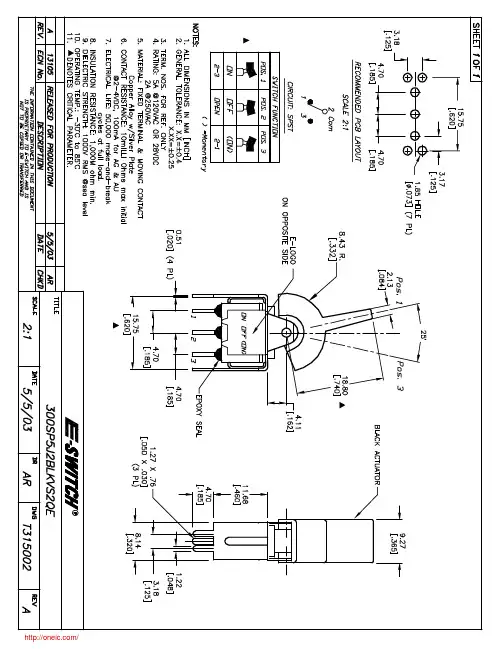
300SP5J2BLKVS2QE;中文规格书,Datasheet资料
- 格式:pdf
- 大小:56.70 KB
- 文档页数:2

Reconfiguration and MultiBootMultiBoot OverviewBecause Spartan®-6 FPGAs are reprogrammable in the system, some applications reloadthe FPGA with one or more bitstream images during normal operation. In this way, asingle smaller FPGA, reprogrammed multiple times, replaces a much larger and moreexpensive ASIC or FPGA programmed just once.A variety of methods can be used to reprogram the FPGA during normal operation. Thedownloaded configuration modes inherently provide this capability. Via an external“intelligent agent,” such as a processor, microcontroller, computer, or tester, an FPGA canbe reprogrammed numerous times. The downloaded modes are available on allSpartan-6FPGA families.Spartan-6 FPGAs include a capability called MultiBoot that allows the FPGA to selectivelyreprogram and reload its bitstream from an attached external memory. The MultiBootfeature allows the FPGA application to load two or more FPGA bitstreams under thecontrol of the FPGA application. The FPGA application triggers a MultiBoot operation,causing the FPGA to reconfigure from a different configuration bitstream. After aMultiBoot operation is triggered, the FPGA restarts its configuration process as usual. TheINIT_B pin pulses Low while the FPGA clears its configuration memory, and the DONEoutput remains Low until the MultiBoot operation successfully completes.MultiBoot is supported in SPI x1, x2, x4, and BPI configuration modes.Spartan-6 FPGA Configuration User Guide UG380 (v2.11) March 22, 2019Chapter 7:Reconfiguration and MultiBootFallback MultiBootFallback BehaviorSpartan-6 FPGAs have dedicated MultiBoot logic, which is used for both fallback and MultiBoot (IPROG) reconfiguration. When fallback or IPROG happens, an internallygenerated pulse resets the entire configuration logic, except for the dedicated MultiBoot logic and the BOOTSTS, MODE, and GENERAL1.5 registers. See Figure 7-1. This reset pulse pulls INIT_B and DONE Low, and restarts the configuration process by clearing configuration memory.During configuration, a CRC error or a watchdog timer time-out error can trigger fallback. The watchdog timer is only active in master configuration modes. The time-out value is user configurable using the BitGen -g TIMER_CFG switch. The switch is followed by a 16-bit value (greater than 16h'0201) indicating the number of configuration clocksallowed before detection of the Sync word times out.During fallback reconfiguration, the FPGA increments the strike count, stored in theBOOTSTS register, and continues reconfiguration if the strike count is less than the limit permitted for that image. If the limit is not reached, the FPGA checks the NEW_MODE bit in the MODE register. If this value is 0, the device uses the configuration mode defined by the mode pins. If the value is 1, the device uses the configuration mode defined in the BOOTMODE bits in the MODE register. The NEW_MODE register is set by the BitGen option -g Next_Config_New_Mode:Yes . The BOOTMODE bits are set by the BitGen option -g Next_Config_Boot_Mode .Figure 7-1:MultiBoot LogicSpartan-6 FPGA Configuration User Guide UG380 (v2.11) March 22, 2019Fallback MultiBootThere are three images for MultiBoot configuration. The first image is the Header. This small bitstream contains the sync word, sets the addresses for the next bitstream as well as the fallback or golden bitstream, and ends with an IPROG command. To generate this bitstream automatically, add the BitGen option -g next_config_addr when creating the programming file for the golden bitstream.The second image is the MultiBoot bitstream. This is the bitstream that the user plans to configure first. The location of this bitstream is defined by the values of GENERAL1,2. The upper eight bits of the GENERAL 2 register are reserved for the opcode for the non-volatile device. See Chapter5, Configuration Details, for more information.The third image is the fallback or golden bitstream. This bitstream is known to be “safe” should an error occur consistently during configuration. The location of this bitstream is defined by the values of GENERAL3,4. As with GENERAL1,2, the upper eight bits of GENERAL4 are reserved for the opcode of the non-volatile device.If the configuration fallback occurs and the golden bitstream is reached, the only way to boot back into the MultiBoot bitstream (located at GENERAL1,2) is to toggle the PROGRAM_B pin, power cycle the device, or use IPROG reconfiguration (see IPROG Reconfiguration, page136)For designs that use more than two bitstreams, the GENERAL1,2 values must be set to the location of the next bitstream then an IPROG command needs to be issued. GENERAL3,4 values should be reserved for the fallback bitstream.The header image must start at address 0. This image has three “strikes” allotted to it. If a CRC error is detected, the strike count increments and configuration restarts if the register setting RESET_ON_ERROR is 1 (located in the register COR2, and can be set from BitGen setting -g Reset_on_err) and the strike count is less than 3. The same behavior occurs if the watchdog timer times out, but it does not depend on RESET_ON_ERROR. The strike counter is found in the BOOTSTS registers. If the count is 3, configuration halts with INIT and DONE driven Low. To clear the strike count, perform a hard reboot (pulse the PROGRAM_B pin) or cycle power.The MultiBoot image can reside at any address specified in GENERAL1,2. This image has three “strikes” allotted to it. If an error is detected, the strike count increments and configuration will restart at the address specified in GENERAL1,2 if the count is less than 3 and RESET_ON_ERROR is 1. If the count hits 3, configuration moves to the fallback bitstream located at GENERAL3,4. There are two ways to clear the strike count: power cycle the FPGA or pulse the PROGRAM_B pin.The fallback (or golden) image can reside at any address specified in GENERAL3,4. This image has 3 strikes allotted to it. If an error is detected, the strike count increments and configuration will restart at the address specified in GENERAL3,4 if the count is less than 6.The value is 6 because it shares the strike counter with the MultiBoot image. If the count reaches 6, configuration boots back to zero, where the header image is located. When this occurs, configuration will attempt both the MultiBoot image and the fallback image three more times before halting configuration. This results in a strike count of 9.After successful fallback reconfiguration, the user design should readback the STATUS or BOOTSTS registers to verify the fallback was successful. Successful fallback configuration maintains the strike count register, and a subsequent soft reboot uses the address stored in GENERAL3,4 (the golden image). There are two ways to clear the strike count: perform a hard reboot (pulse the PROGRAM_B pin) or cycle power.If fallback reconfiguration exhausts all three strikes out, configuration stops and both INIT_B and DONE are held Low.Fallback is disabled if AES is enabled and for Slave configuration mode.Spartan-6 FPGA Configuration User Guide UG380 (v2.11) March 22, 2019Chapter 7:Reconfiguration and MultiBootIPROG ReconfigurationThe IPROG (internal PROGRAM_B) command has similar effect as a pulsingPROGRAM_B pin, except IPROG does not reset the dedicated reconfiguration logic. The start address set in GENERAL1,2 is used during reconfiguration instead of the default address (zero). The fallback (golden) bitstream address is set in GENERAL3,4. The IPROG command can be sent through ICAP_SPARTAN6 or the bitstream.Reboot Using ICAP_SPARTAN6The IPROG command can also be sent using the ICAP_SPARTAN6 primitive. After a successful configuration, the user design determines the start address of the MultiBoot bitstream, and sets the GENERAL1,2 registers, and then issues an IPROG command using ICAP.The sequence of commands is:1.Send the Sync word.2.Program the GENERAL1,2 registers for the next bitstream start address and the non-volatile device opcode for a read operation. Also program the GENERAL3,4 registersfor the fallback (golden) bitstream start address and the opcode for the non-volatiledevice for a read operation.3.Send the IPROG command.Table 7-1 shows an example bitstream for the IPROG command using ICAP.Table 7-1:Example Bitstream for IPROG through ICAP ConfigurationData (hex)(1)Explanation FFFFDummy Word AA99Sync Word 5566Sync Word 3261Type 1 Write 1 Words to GENERAL_1XXXXMultiBoot Start Address [15:0]3281Type 1 Write 1 Word to GENERAL2(2)XXXXOpcode and MultiBoot Start Address [23:16]32A1Type 1 Write 1 Word to GENERAL3XXXXFallback Start Address [15:0]32C1Type 1 Write 1 Word to GENERAL4(2)XXXXOpcode and Fallback Start Address [23:16]30A1Type 1 Write 1 Word to CMD 000EIPROG Command 2000Type 1 NO OPNotes:1.SelectMAP 16-bit data ordering applies to the ICAP data bus. See Table 2-5, page 40 for proper bit ordering.2.The eight most significant bits of GENERAL2 and GENERAL4 registers represent the opcode for the read instruction for the non-volatile storage device. Consult the data sheet of the storage device for the proper opcode. Common codes are 0x0B , 0x3B , and 0x6B for Fast Read, Dual Fast Read, and Quad Fast Read, respectively.Spartan-6 FPGA Configuration User Guide UG380 (v2.11) March 22, 2019Status Register for Fallback and IPROG ReconfigurationAfter the configuration logic receives the IPROG command, the FPGA resets everythingexcept the dedicated reconfiguration logic, and the INIT_B and DONE pins go Low. Afterthe FPGA clears all configuration memory, INIT_B goes High again. Then the value inGENERAL1,2 is used for the bitstream starting address.IPROG does not reset the strike count. MultiBoot applications that use IPROG throughICAP_SPARTAN6 should pulse PROGRAM_B or implement a power cycle after aconfiguration error that increments the strike count. Otherwise, verify that externalmemory is properly updated to avoid configuration errors that would increment the strikecount.Status Register for Fallback and IPROG ReconfigurationSpartan-6 devices contain a BOOTSTS that stores configuration history. At EOS or an errorcondition, Status_0 is updated with the current status. If fallback or MultiBoot occurs,Status_1 is updated at EOS or an error condition. The Valid_0 bit indicates if the rest ofStatus_0 is valid or not. The BOOTSTS register is written either at an End Of Startup (EOS)event or a fallback event. The EOS event happens after the first configuration attempt. Asuccessful MultiBoot operation via the IPROG command does not result in the BOOTSTSregister being updated. See Boot History Status Register (BOOTSTS), page110.Table7-2 through Table7-4show the BOOTSTS values in some common situations.Table 7-2:Status after First Bitstream Configuration without ErrorCRC_ERROR ID_ERROR WTO_ERROR IPROG FALLBACK VALID Status_1000000Status_0000001Table 7-3:First Configuration followed by IPROGCRC_ERROR ID_ERROR WTO_ERROR IPROG FALLBACK VALID Status_1000001Status_0000101Table 7-4:IPROG Embedded in First Bitstream, Second Bitstream CRC Error, andFallback SuccessfullyCRC_ERROR(1)ID_ERROR WTO_ERROR IPROG FALLBACK VALID Status_1(2)000111Status_0(3)100101Notes:1.CRC_Error only registers CRC errors detected during initial configuration. CRC_Error is not updatedif CRC errors are found from the Readback CRC (POST_CRC) function.2.Status_1 shows a fallback bitstream was loaded successfully. The IPROG bit was also set in this case,because the fallback bitstream contains an IPROG command. Although the IPROG command isignored during fallback, the status still records this occurrence.3.Status_0 shows IPROG was attempted, and a CRC_ERROR was detected for that bitstream.。

BYV32EX-300PDual ultrafast power diodeRev.01 13 March 2019Product data sheet1. General descriptionUltrafast power diode in a SOT186A (TO-220F) plastic package.2. Features and benefits• Ultra low leakage current• High junction temperature up to 175 °C• Low on-state loss• Fast switching• Soft recovery characteristic minimizes power consuming oscillations• High reverse surge capability• High thermal cycling performance• Low thermal resistance3. Applications• Home appliance power supply• Secondary rectification4. Quick reference data5. Pinning information6. Ordering information7. Marking8. Limiting values Table 5. Limiting values9. Thermal characteristics10. Isolation characteristics11. Characteristics12. Package outline13. Legal informationData sheet status[1lease consult the most recently issued document before initiating or completing a design.[2]The term 'short data sheet' is explained in section "Definitions".[3]The product status of device(s) described in this document may havechanged since this document was published and may differ in case ofmultiple devices. The latest product status information is available onthe Internet at URL .DefinitionsDraft — The document is a draft version only. The content is still under internal review and subject to formal approval, which may result in modifications or additions. WeEn Semiconductors does not give any representations or warranties as to the accuracy or completeness of information included herein and shall have no liability for the consequences of use of such information.Short data sheet — A short data sheet is an extract from a full data sheet with the same product type number(s) and title. A short data sheet is intended for quick reference only and should not be relied upon to contai n detailed and full information. For detailed and full information see the relevant full data sheet, which is available on request via the local WeE n Semiconductors sales office. In case of any inconsistency or conflict with the short data sheet, the full data sheet shall prevail.Product specification — The information and data provided in a Product data sheet shall define the specification of the product as agreed between WeEn Semiconductors and its customer, unless WeEn Semiconductors and customer have explicitly agreed otherwise in writing. In no event however, shall an agreement be valid in which the WeEn Semiconductors productis deemed to offer functions and qualities beyond those described in the Product data sheet.DisclaimersLimited warranty and liability — Information in this document is believedto be accurate and reliable. However, WeEn Semiconductors does notgive any representations or warranties, expressed or implied, as to the accuracy or completeness of such information and shall have no liability for the consequences of use of such information. WeEn Semiconductors takes no responsibility for the content in this document if provided by an information source outside of WeEn Semiconductors.In no event shall WeEn Semiconductors be liable for any indirect, incidental, punitive, special or consequential damages (including - without limitation -lost profits, lost savings, business interruption, costs related to the removal or replacement of any products or rework charges) whether or not such damages are based on tort (including negligence), warranty, breach of contract or any other legal theory.Notwithstanding any damages that customer might incur for any reason whatsoever, WeEn Semiconductors’ aggregate and cumulative liability towards customer for the products described herein shall be limited in accordance with the Terms and conditions of commercial sale of WeEn Semiconductors.Right to make changes — WeEn Semiconductors reserves the right to make changes to information published in this document, including without limitation specifications and product descriptions, at any time and without notice. This document supersedes and replaces all information supplied prior to the publication hereof.Suitability for use — WeEn Semiconductors products are not designed, authorized or warranted to be suitable for use in life support, life-criticalor safety-critical systems or equipment, nor in applications where failureor malfunction of an WeEn Semiconductors product can reasonablybe expected to result in personal injury, death or severe property or environmental damage. WeEn Semiconductors and its suppliers accept no liability for inclusion and/or use of WeEn Semiconductors products in such equipment or applications and therefore such inclusion and/or use is at th e customer’s own risk.Quick reference data — The Quick reference data is an extract of the product data given in the Limiting values and Characteristics sections of this document, and as such is not complete, exhaustive or legally binding. Applications — Applications that are described herein for any of these products are for illustrative purposes only. WeEn Semiconductors makesno representation or warranty that such applications will be suitable for the specified use without further testing or modification.Customers are responsible for the design and operation of their applications and products using WeEn Semiconductors products, and WeEn Semiconductors accepts no liability for any assistance with applications or customer product design. It is customer’s sole responsibility to determine whether the WeEn Semiconductors product is suitable and fit for the customer’s applications and products planned, as well as for the planned application and use of customer’s third party customer(s). Customers should provide appropriate design and operating safeguards to minimize the risks associated with their applications and products.WeEn Semiconductors does not accept any liability related to any default, damage, costs or problem which is based on any weakness or defaultin the customer’s applications or products, or the application or use by customer’s third party customer(s). Customer is responsible for doing all necessary testing for the customer’s applications and products using WeEn Semiconductors products in order to avoid a default of the applicationsand the products or of the application or use by customer’s third party customer(s). WeEn does not accept any liability in this respect.Limiting values — Stress above one or more limiting values (as defined in the Absolute Maximum Ratings System of IEC 60134) will cause permanent damage to the device. Limiting values are stress ratings only and (proper) operation of the device at these or any other conditions above thosegiven in the Recommended operating conditions section (if present) or the Characteristics sections of this document is not warranted. Constant or repeated exposure to limiting values will permanently and irreversibly affect the quality and reliability of the device.No offer to sell or license — Nothing in this document may be interpreted or construed as an offer to sell products that is open for acceptance or the grant, conveyance or implication of any license under any copyrights, patents or other industrial or intellectual property rights.Export control — This document as well as the item(s) described herein may be subject to export control regulations. Export might require a prior authorization from competent authorities.Non-automotive qualified products — Unless this data sheet expressly states that this specific WeEn Semiconductors product is automotive qualified, the product is not suitable for automotive use. It is neither qualifie d nor tested in accordance with automotive testing or application requirements. WeEn Semiconductors accepts no liability for inclusion and/or use of non-automotive qualified products in automotive equipment or applications.In the event that customer uses the product for design-in and use in automotive applications to automotive specifications and standards, customer (a) shall use the product without WeEn Semiconductors’ warranty of the product for such automotive applications, use and specifications, and (b) whenever customer uses the product for automotive applications beyond WeEn Semiconductors’ specifications such use shall be solely at customer’s own risk, and (c) customer fully indemnifies WeEn Semiconductors forany liability, damages or failed product claims resulting from customer design and use of the product for automotive applications beyond WeEn Semiconductors’ standard warranty and WeEn Semiconductors’ product specifications.]PTranslations — A non-English (translated) version of a document is for reference only. The English version shall prevail in case of any discrepancy between the translated and English versions.TrademarksNotice: All referenced brands, product names, service names and trademarks are the property of their respective owners.14. Contents1. General description (1)2. Features and benefits (1)3. Applications (1)4. Quick reference data (1)5. Pinning information (2)6. Ordering information (2)7. Marking (2)8. Limiting values (3)9. Thermal characteristics (5)10. Isolation characteristics (5)11. Characteristics (6)12. Package outline (7)13. Legal information (8)14. Contents (10)© WeEn Semiconductors Co., Ltd. 2019. All rights reservedFor more information, please visit: Forsalesofficeaddresses,pleasesendanemailto:**************************** Date of release: 13 March 2019。

300P A N D U A N P E N G G U N APENDAHULUAN (1)ISI KOTAK (2)GAMBARAN UMUM PRODUK (3)Kontrol pada headset (3)MULAI MENGGUNAKAN (4)Menggunakan headset (4)Pengaturan penggunaan pertama (khusus untuk PC) (4)MENGGUNAKAN HEADSET (6)Dengan sambungan USB (6)Dengan koneksi audio 3,5 mm (7)SPESIFIKASI PRODUK (8)PEMECAHAN MASALAH (9)Selamat atas pembelian Anda! Manual ini mencakup informasi tentang headset game JBL QUANTUM300. Kami sarankan Anda meluangkan diri untuk membaca panduan ini, yang isinya berupa penjelasan produk dan petunjuk untuk membantu Anda menyiapkan dan memulai pemakaian. Baca dan pahami semua petunjuk keselamatan sebelum menggunakan produk.Jika Anda memiliki pertanyaan tentang produk atau operasi produk ini,silakan hubungi pengecer atau layanan pelanggan, atau kunjungi kami di .0304010201 Headset JBL QUANTUM30002 Adaptor audio USB03 Kartu garansi dan lembar keselamatan QSG04 Busa penahan angin untuk mikrofon boomKontrol pada headset01 Dial volume +/-• Menyesuaikan volume headset.02 Busa penahan angin yang dapat dilepas03 Mikrofon boom fokus suara• Putar ke atas atau ke bawah untuk mengaktifkan mikrofon.04 Ear cup Flat yang dapat dilipatMenggunakan headset1. Pastikan sisi bertanda L dipasang ke telinga kiri dan sisi bertanda R dipasang ketelinga kanan.2. Sesuaikan bantalan telinga dan headband agar nyaman dipakai.3. Sesuaikan mikrofon jika perlu.Pengaturan penggunaan pertama (khusus untuk PC) Unduh (/engine) untuk mendapatkan akses ke teknologi audio 3D Quantum.Persyaratan perangkat lunakPlatform: Windows 7/Windows 10 (64 bit) saja500 MB ruang bebas di hard drive untuk penginstalanKIAT:• QuantumSURROUND dan DTS Headphone:X V2.0 hanya tersedia untuk Windows. Memerlukan penginstalan perangkat lunak.1. Hubungkan headset ke PC via sambungan USB (Lihat “Dengan sambungan USB”).2. Masuk ke “Sound Settings” -> “Sound Control Panel”.3. Pada “Playback” soroti “JBL QUANTUM300” dan pilih “Set Default”.4. Pada “Recording” soroti “JBL QUANTUM300” dan pilih “Set Default”.5. Pada aplikasi obrolan Anda, pilih “JBL QUANTUM300” s ebagai perangkat audiostandar.6. Ikuti petunjuk pada layar untuk personalisasi pengaturan suara Anda.Dengan sambungan USB1. Sambungkan konektor USB pada adaptor audio USB dengan porta USB-A padaPC atau Mac Anda.2. Sambungkan konektor 3,5 mm pada headset Anda dengan adaptor audio USB. Operasi dasarKontrol PengoperasianDial volume Menyesuaikan volume master.Dengan koneksi audio 3,5 mmSambungkan konektor 3,5 mm pada headset Anda dengan jack pada PC, Mac, atau perangkat seluler serta konsol game.Operasi dasarKontrol PengoperasianDial volume Menyesuaikan volume master.• Ukuran driver: Driver Dinamis 50 mm• Respons frekuensi: 20 Hz - 20 kHz• Daya input maks. 30 mW• Sensitivitas: 100 dB SPL @1 kHz/1 mW• Impedansi: 32 ohm• Respon frekuensi mikrofon: 100 Hz - 10 KHz• sensitivitas mikrofon: -40 dBV @1 kHz/Pa• Pola pickup mikrofon: Dapat diarahkan• Ukuran mikrofon: 4 mm x 1,5 mm• Panjang kabel: Headset (1,2 m) + Adaptor audio USB (1,5 m)• Berat: 245 gCATATAN:• Spesifikasi teknis dapat berubah sewaktu-waktu tanpa pemberitahuan.Jika Anda mengalami masalah dalam penggunaan produk ini, bacalah poin-poin berikut ini sebelum mengajukan permintaan layanan.Tidak ada suara atau kualitas suara buruk• Pastikan Anda sudah memilih JBL QUANTUM300 sebagai perangkat standar pengaturan suara game pada PC, Mac, atau perangkat konsol game Anda.• Sesuaikan volume pada PC, Mac, atau perangkat konsol game Anda.Pada sambungan USB:• Pastikan USB dan koneksi audio 3,5 mm tidak goyah.• Kemungkinan porta USB pada sebagian perangkat konsol game tidak kompatibel dengan JBL QUANTUM300. Ini bukan kegagalan fungsi perangkat. Pada koneksi audio 3,5 mm:• Pastikan koneksi audio 3,5 mm tidak goyah.Suara saya tidak dapat didengar teman• Pastikan Anda sudah memilih JBL QUANTUM300 sebagai perangkat standar pengaturan suara obrolan pada PC, Mac, atau perangkat konsol game Anda.• Pastikan mikrofon tidak dimatikan.- 9 -HP_JBL_Q300_OM_V3。

PRODUCTION DATA information is current as of publication date. Products conform to specifications per the terms of Texas Instruments standard warranty. Production processing does not necessarily include testing of all parameters.元器件交易网IMPORTANT NOTICETexas Instruments and its subsidiaries (TI) reserve the right to make changes to their products or to discontinueany product or service without notice, and advise customers to obtain the latest version of relevant informationto verify, before placing orders, that information being relied on is current and complete. All products are soldsubject to the terms and conditions of sale supplied at the time of order acknowledgement, including thosepertaining to warranty, patent infringement, and limitation of liability.TI warrants performance of its semiconductor products to the specifications applicable at the time of sale inaccordance with TI’s standard warranty. Testing and other quality control techniques are utilized to the extentTI deems necessary to support this warranty. Specific testing of all parameters of each device is not necessarilyperformed, except those mandated by government requirements.CERTAIN APPLICATIONS USING SEMICONDUCTOR PRODUCTS MAY INVOLVE POTENTIAL RISKS OFDEATH, PERSONAL INJURY, OR SEVERE PROPERTY OR ENVIRONMENTAL DAMAGE (“CRITICALAPPLICATIONS”). TI SEMICONDUCTOR PRODUCTS ARE NOT DESIGNED, AUTHORIZED, ORWARRANTED TO BE SUITABLE FOR USE IN LIFE-SUPPORT DEVICES OR SYSTEMS OR OTHERCRITICAL APPLICATIONS. INCLUSION OF TI PRODUCTS IN SUCH APPLICATIONS IS UNDERSTOOD TOBE FULLY AT THE CUSTOMER’S RISK.In order to minimize risks associated with the customer’s applications, adequate design and operatingsafeguards must be provided by the customer to minimize inherent or procedural hazards.TI assumes no liability for applications assistance or customer product design. TI does not warrant or representthat any license, either express or implied, is granted under any patent right, copyright, mask work right, or otherintellectual property right of TI covering or relating to any combination, machine, or process in which suchsemiconductor products or services might be or are used. TI’s publication of information regarding any thirdparty’s products or services does not constitute TI’s approval, warranty or endorsement thereof.Copyright © 1999, Texas Instruments Incorporated。