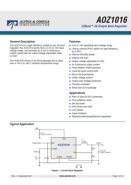
AOZ1081AI;中文规格书,Datasheet资料
- 格式:pdf
- 大小:1009.79 KB
- 文档页数:11
General DescriptionThe AOZ1081 is a high efficiency, simple to use, 1.8A buck regulator for White LED. The AOZ1081 works from a 4.5V to 16V input voltage range, and provides up to 1.8A of continuous output current with an output voltage adjustable down to 0.25V.The AOZ1081 comes in an SO-8 package and is rated over a -40°C to +85°C ambient temperature range.Features●4.5V to 16V operating input voltage range ●100 m Ω internal PFET switch for high efficiency: up to 95%●Internal Schottky Diode ●Internal soft start●0.25V internal reference with ±5% accuracy over temperature●1.8A continuous output current ●Fixed 1MHz PWM operation ●Cycle-by-cycle current limit ●Short-circuit protection ●Under voltage lockout ●Output over voltage protection ●Thermal shutdown ●Small size SO-8 packageApplications●Buck regulator for white LEDs ●Landscape lighting ●Flashlights●Battery powered backlight applicationsTypical ApplicationFigure 1.Figure 2.Ordering InformationAll AOS products are offered in packages with Pb-free plating and compliant to RoHS standards.Please visit /web/quality/rohs_compliant.jsp for additional information.Part NumberAmbient Temperature RangePackageEnvironmentalAOZ1081AI-40°C to +85°CSO-8RoHSPin ConfigurationPin DescriptionPinNumber Pin Name Pin Function1PGND Power ground. Electrically needs to be connected to AGND.2VIN Supply voltage input. When V IN rises above the UVLO threshold the device starts up.3AGND Reference connection for controller section. Also used as thermal connection for controllersection. Electrically needs to be connected to PGND.4FB LED Current Feedback Input. The FB voltage is regulated at 250mV in normal operation. The FBsense resistor sets the nominal LED current5COMP External loop compensation pin.6EN The enable pin is active high. Connect EN pin to V IN if not used. Do not leave the EN pin floating.7,8LX PWM output connection to inductor. Thermal connection for output stage.Block DiagramAbsolute Maximum RatingsExceeding the Absolute Maximum Ratings may damage the device.Note:1. Devices are inherently ESD sensitive, handling precautions are required. Human body model rating: 1.5kΩ in series with 100pF.Recommend Operating RatingsThe device is not guaranteed to operate beyond the Maximum Operating Ratings.Note:2. The value of ΘJA is measured with the device mounted on 1-in2FR-4 board with 2oz. Copper, in a still air environment with T A = 25°C. The value in any given application depends on the user's spe-cific board design.Parameter RatingSupply Voltage (V IN)18V LX to AGND-0.7V to V IN+0.3V EN to AGND-0.3V to V IN+0.3V FB to AGND-0.3V to 6V COMP to AGND-0.3V to 6V PGND to AGND-0.3V to +0.3V Junction Temperature (T J)+150°C Storage Temperature (T S)-65°C to +150°C ESD Rating(1)2kVParameter Rating Supply Voltage (V IN) 4.5V to 16V Output Voltage Range0.25V to V IN Ambient Temperature (T A)-40°C to +85°C Package Thermal Resistance SO-8(ΘJA)(2)87°C/WElectrical CharacteristicsT A = 25°C, V IN = V EN = 12V, V OUT = 3.3V unless otherwise specified (3)Note:3. Specification in BOLD indicate an ambient temperature range of -40°C to +85°C. These specifications are guaranteed by design.SymbolParameterConditions Min.Typ.Max.UnitsV IN Supply Voltage4.516V V UVLO Input Under-Voltage Lockout ThresholdV IN Rising V IN Falling4.03.7VI IN Supply Current (Quiescent)I OUT = 0, V COMP = 0.1V, V EN >1.2V 23mA I OFF Shutdown Supply Current V EN = 0V110µA V FBFeedback Voltage 0.23750.250.2625V Load Regulation 0.5%Line Regulation0.5%I FB Feedback Voltage Input Current 200nA V EN EN Input Threshold Off Threshold On Threshold2.00.6V V HYS EN Input Hysteresis 100mVMODULATORf O Frequency85010001150kHz D MAX Maximum Duty Cycle 100%D MINMinimum Duty Cycle 12%Error Amplifier Voltage Gain 500V / V Error Amplifier Transconductance200µA / VPROTECTIONI LIM Current Limit2.54.0A V PR Output Over-Voltage Protection ThresholdOff Threshold On Threshold330240mV T J Over-Temperature Shutdown Limit 150°C t SSSoft Start Interval400µsOUTPUT STAGEHigh-Side Switch On-ResistanceV IN = 12V V IN = 5V97166130200m ΩTypical Performance CharacteristicsCircuit of Figure 1. T A = 25°C, V IN = V EN = 12V, V OUT = 3.3V unless otherwise specified.Typical Performance Characteristics (Continued)0.5A/DivPWM Dimming at 200Hz (90% Duty Cycle)0.5A/DivPWM Dimming at 200Hz (90% Duty Cycle)0.5A/Div Start Up2.5V/DivDetailed DescriptionThe AOZ1081 is a current-mode step down regulator with integrated high side PMOS switch and a low side freewheeling Schottky diode. It operates from a 4.5V to 16V input voltage range and supplies up to 1.8A of load current. The duty cycle can be adjusted from 12% to 100% allowing a wide range of output voltage. Features include enable control, Power-On Reset, input under voltage lockout, fixed internal soft-start and thermal shut down.The AOZ1081 is available in SO-8 package.Enable and Soft StartThe AOZ1081 has internal soft start feature to limitin-rush current and ensure the output voltage ramps up smoothly to regulation voltage. A soft start process begins when the input voltage rises to 4.5V and voltage on EN pin is HIGH. In soft start process, the output volt-age is ramped to regulation voltage in typically 400µs. The 400µs soft start time is set internally.The EN pin of the AOZ1081 is active HIGH. Connect the EN pin to V IN if enable function is not used. Pull it to ground will disable the AOZ1081. Do not leave it open. The voltage on EN pin must be above 2.0 V to enable the AOZ1081. When voltage on EN pin falls below 0.6V, the AOZ1081 is disabled. If an application circuit requires the AOZ1081 to be disabled, an open drain or open collector circuit should be used to interface to EN pin.PWM DimmingThe AOZ1081 allows dimming up to 200Hz PWM signal at the EN pin. By forcing a PWM digital waveform to the EN pin, the system will go into a digital dimming state. The output switch will be off when PWM waveform is logic low and it will be on when PWM waveform is logic high. The duty cycle range is 10% to 100%.Steady-State OperationUnder steady-state conditions, the converter operatesin fixed frequency and Continuous-Conduction Mode (CCM).The AOZ1081 integrates an internal P-MOSFET as the high-side switch. Inductor current is sensed by amplifying the voltage drop across the drain to source of the high side power MOSFET. Output voltage is divided down by the external voltage divider at the FB pin. The difference of the FB pin voltage and reference is amplified by the internal transconductance error amplifier. The error volt-age, which shows on the COMP pin, is compared against the current signal, which is sum of inductor current signal and ramp compensation signal, at PWM comparator input. If the current signal is less than the error voltage, the internal high-side switch is on. The inductor current flows from the input through the inductor to the output. When the current signal exceeds the error voltage, the high-side switch is off. The inductor current is freewheel-ing through the internal Schottky diode to output.The AOZ1081 uses a P-Channel MOSFET as the high side switch. It saves the bootstrap capacitor normally seen in a circuit which is using an NMOS switch. It allows 100% turn-on of the upper switch to achieve linear regulation mode of operation. The minimum voltage drop from V IN to V O is the load current times DC resistance of MOSFET + DC resistance of buck inductor. It can be calculated by equation below:where,V O_MAX is the maximum output voltage;V IN is the input voltage from 4.5V to 16V;I O is the output current from 0A to 1.8A;R DS(ON) is the on resistance of internal MOSFET, the value is between 97mΩ and 200mΩ depending on input voltage and junction temperature; andR inductor is the inductor DC resistance;Switching FrequencyThe AOZ1081 switching frequency is fixed and set by an internal oscillator. The actual switching frequency could range from 850kHz to 1.15MHz due to device variation. Protection FeaturesThe AOZ1081 has multiple protection features to prevent system circuit damage under abnormal conditions. Over Current Protection (OCP)The sensed inductor current signal is also used for over current protection. Since the AOZ1081 employs peak current mode control, the COMP pin voltage is propor-tional to the peak inductor current. The COMP pin volt-age is limited to be between 0.4V and 2.5V internally. The peak inductor current is automatically limited cycle by cycle.The cycle by cycle current limit threshold is set between 2.5A and 4A. When the load current reaches the current limit threshold, the cycle by cycle current limit circuit turns V O_MAX V IN I O R DS ON()R inductor+()×–=off the high side switch immediately to terminate the current duty cycle. The inductor current stop rising.The cycle by cycle current limit protection directly limits inductor peak current. The average inductor current is also limited due to the limitation on peak inductor current. When cycle by cycle current limit circuit is triggered, the output voltage drops as the duty cycle decreasing.The AOZ1081 has internal short circuit protection to protect itself from catastrophic failure under output short circuit conditions. The FB pin voltage is proportional to the output voltage. Whenever FB pin voltage is below 0.15V, the short circuit protection circuit is triggered.As a result, the converter is shut down and hiccups at a frequency equals to 1/8 of normal switching frequency. The converter will start up via a soft start once the short circuit condition disappears. In short circuit protection mode, the inductor average current is greatly reduced because of the low hiccup frequency.Output Over Voltage Protection (OVP)The AOZ1081 monitors the feedback voltage: when the feedback voltage is higher than 330mV, it immediate turns-off the PMOS to protect the output voltage over-shoot at fault condition. When feedback voltage is lower than 240mV, the PMOS is allowed to turn on in the next cycle.Power-On Reset (POR)A power-on reset circuit monitors the input voltage. When the input voltage exceeds 4V, the converter starts opera-tion. When input voltage falls below 3.7V, the converter will stop switching.Thermal ProtectionAn internal temperature sensor monitors the junction temperature. It shuts down the internal control circuit and high side PMOS if the junction temperature exceeds 150°C.Application InformationThe basic AOZ1081 application circuit is shown in Figure 1 and 2. Component selection is explained below. Setting the Maximum LED CurrentThe AOZ1081 features a programmable LED current using a resistor R FB at the end of the primary chain of LEDs.Input CapacitorThe input capacitor (C1 in Figure 1) must be connected to the V IN pin and PGND pin of the AOZ1081 to maintain steady input voltage and filter out the pulsing input current. A small decoupling capacitor (Cd in Figure 1), usually 1µF, should be connected to the V IN pin and AGND pin for stable operation of the AOZ1081. The voltage rating of input capacitor must be greater than maximum input voltage plus ripple voltage.The input ripple voltage can be approximated by equa-tion below:Since the input current is discontinuous in a buck converter, the current stress on the input capacitor is another concern when selecting the capacitor. For a buck circuit, the RMS value of input capacitor current can be calculated by:if let m equal the conversion ratio:The relationship between the input capacitor RMS current and voltage conversion ratio is calculated and shown in Figure 2. It can be seen that when V O is half of V IN, C IN is under the worst current stress. The worst current stress on C IN is 0.5 x I O.Figure 2. I CIN vs. Voltage Conversion RatioI LEDMAX250mVR FB-------------------=ΔV INI Of C IN×-----------------1V OV IN--------–⎝⎠⎜⎟⎛⎞V OV IN--------××=I CIN_RMS I OV OV IN--------1V OV IN--------–⎝⎠⎜⎟⎛⎞×=V OV IN--------m=For reliable operation and best performance, the input capacitors must have current rating higher than I CIN_RMS at worst operating conditions. Ceramic capacitors are preferred for input capacitors because of their low ESR and high ripple current rating. Depending on the application circuits, other low ESR tantalum capacitoror aluminum electrolytic capacitor may also be used. When selecting ceramic capacitors, X5R or X7R type dielectric ceramic capacitors are preferred for their better temperature and voltage characteristics. Note that the ripple current rating from capacitor manufactures is based on certain amount of life time. Further de-rating may be necessary for practical design requirement. InductorThe inductor is used to supply constant current to output when it is driven by a switching voltage. For given input and output voltage, inductance and switching frequency together decide the inductor ripple current, which is: The peak inductor current is:High inductance gives low inductor ripple current but requires larger size inductor to avoid saturation. Low ripple current reduces inductor core losses. It also reduces RMS current through inductor and switches, which results in less conduction loss. Usually, peak to peak ripple current on inductor is designed to be 20%to 30% of output current.When selecting the inductor, make sure it is able to handle the peak current without saturation even at the highest operating temperature.The inductor takes the highest current in a buck circuit. The conduction loss on inductor needs to be checked for thermal and efficiency requirements.Surface mount inductors in different shape and styles are available from Coilcraft, Elytone and Murata. Shielded inductors are small and radiate less EMI noise. But they cost more than unshielded inductors. The choice depends on EMI requirement, price and size.Output CapacitorThe output capacitor is selected based on the DC output voltage rating, output ripple voltage specification and ripple current rating.The selected output capacitor must have a higherrated voltage specification than the maximum desired output voltage including ripple. De-rating needs to be considered for long term reliability.Output ripple voltage specification is another important factor for selecting the output capacitor. In a buck converter circuit, output ripple voltage is determined by inductor value, switching frequency, output capacitor value and ESR. It can be calculated by the equation below:where;C O is output capacitor value, andESR CO is the Equivalent Series Resistor of output capacitor. When low ESR ceramic capacitor is used as output capacitor, the impedance of the capacitor at the switch-ing frequency dominates. Output ripple is mainly caused by capacitor value and inductor ripple current. The output ripple voltage calculation can be simplified to:If the impedance of ESR at switching frequency dominates, the output ripple voltage is mainly decided by capacitor ESR and inductor ripple current. The output ripple voltage calculation can be further simplified to: For lower output ripple voltage across the entire operating temperature range, X5R or X7R dielectric type of ceramic, or other low ESR tantalum are recommended to be used as output capacitors.In a buck converter, output capacitor current is continuous. The RMS current of output capacitor is decided by the peak to peak inductor ripple current.It can be calculated by:Usually, the ripple current rating of the output capacitor is a smaller issue because of the low current stress. When the buck inductor is selected to be very small and inductor ripple current is high, output capacitor could be overstressed.ΔI LV Of L×----------1V OV IN--------–⎝⎠⎜⎟⎛⎞×=I Lpeak I OΔI L2 --------+=ΔV OΔI L ESR CO18f C O××-------------------------+⎝⎠⎛⎞×=ΔV OΔI L18f C O××-------------------------×=ΔV OΔI L ESR CO×=I CO_RMSΔI L12----------=分销商库存信息: AOSAOZ1081AI。