
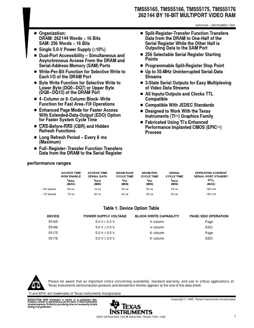
TMS55166中文资料
- 格式:pdf
- 大小:1.51 MB
- 文档页数:70
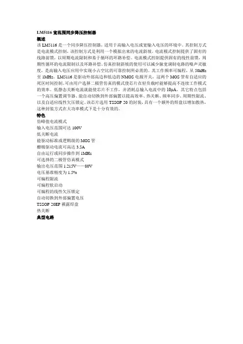
LM5116宽范围同步降压控制器概述该LM5116是一个同步降压控制器,适用于高输入电压或宽输入电压的环境中。
其控制方式是电流模式控制,该控制方式是利用一个模拟出来的电流斜坡。
电流模式控制提供了固有的线路前馈,以周期电流限制和易于循环的环路补偿。
电流模式控制提供固有的线性前馈,周期性循环的电流限制以及环路补偿。
仿真控制斜坡的使用可以减少脉宽调制电路的噪声灵敏度,是高输入电压应用中实现小占空比的可靠控制所必需的。
其工作频率可编程,从50kHz 至1MHz。
LM5116是驱动外部高边和低边的NMOS电源开关,这两个MOS管有自适应的死区时间控制。
可由用户选择二极管仿真的模式使芯片在轻负载时能够提高不连续工作模式的效率。
低静态关断电流就能使芯片不工作,并消耗总输入电流中的10μA。
其它特点包括一个高压偏置调节器、能自动切换到外部偏置以提高效率、热关断、频率同步、周期性限流、以及自适应线性欠压锁定。
该芯片选用TSSOP-20的封装,具有一个额外的焊盘以增加散热,这种封装方式在大功率模式下是十分有效的。
特色仿峰值电流模式输入电压范围可达100V低关断电流能驱动标准或逻辑级的MOS管栅极驱动电流可高达3.5A自由运行或同步操作到1MHz可选择的二极管仿真模式输出电压范围1.215V——80V电压基准精度为1.5%可编程限流可编程软启动可编程的线性欠压锁定自动切换到外部偏置电压TSSOP-20EP裸露焊盘热关断典型电路引脚名称描述1 VIN 芯片电源电压,输入电压2 UVLO 如果UVLO引脚的电压低于1.215V,调节器会进入待机模式(VCC调节器工作,开关驱动电路不工作)。
如果UVLO引脚电压高于1.215V,这个调节器正常工作。
可以通过外部分压器来设置欠压关断的阈值。
当EN引脚为高时,这个引脚存在一个固定的5μA上拉电流。
在工作在电流限制模式时,UVLO会每隔256个时钟周期被拉到地。
3 RT/SYNC 内部晶振可以通过一个该引脚和地之间的电阻来设置。
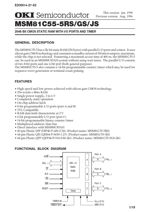
T M S320F28335中文资料TMS320F28335中文资料TMS320F28335采用176引脚LQFP四边形封装,其功能结构参见参考文献。
其主要性能如下:高性能的静态CMOS技术,指令周期为6.67 ns,主频达150 MHz;高性能的32位CPU,单精度浮点运算单元(FPU),采用哈佛流水线结构,能够快速执行中断响应,并具有统一的内存管理模式,可用C/C++语言实现复杂的数学算法;6通道的DMA控制器;片上256 Kxl6的Flash存储器,34 Kxl6的SARAM存储器.1 Kx16 OTPROM和8 Kxl6的Boot ROM。
其中Flash,OTPROM,16 Kxl6的SARAM均受密码保护;控制时钟系统具有片上振荡器,看门狗模块,支持动态PLL调节,内部可编程锁相环,通过软件设置相应寄存器的值改变CPU的输入时钟频率;8个外部中断,相对TMS320F281X系列的DSP,无专门的中断引脚。
GPI00~GPI063连接到该中断。
GPI00一GPI031连接到XINTl,XINT2及XNMI外部中断,GPl032~GPI063连接到XINT3一XINT7外部中断;支持58个外设中断的外设中断扩展控制器(PIE),管理片上外设和外部引脚引起的中断请求;增强型的外设模块:18个PWM输出,包含6个高分辨率脉宽调制模块(HRPWM)、6个事件捕获输入,2通道的正交调制模块(QEP);3个32位的定时器,定时器0和定时器1用作一般的定时器,定时器0接到PIE模块,定时器1接到中断INTl3;定时器2用于DSP/BIOS的片上实时系统,连接到中断INTl4,如果系统不使用DSP/BIOS,定时器2可用于一般定时器;串行外设为2通道CAN模块、3通道SCI模块、2个McBSP(多通道缓冲串行接口)模块、1个SPI模块、1个I2C主从兼容的串行总线接口模块;12位的A/D转换器具有16个转换通道、2个采样保持器、内外部参考电压,转换速度为80 ns,同时支持多通道转换;88个可编程的复用GPIO引脚;低功耗模式;1.9 V内核,3.3 V I/O供电;符合IEEEll49.1标准的片内扫描仿真接口(JTAG);TMS320F28335的存储器映射需注意以下几点:片上外设寄存器块0~3只能用于数据存储区,用户不能在该存储区内写入程序。

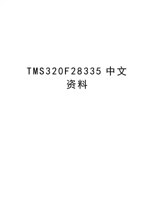
2F, No.10, Prosperity RD. II, Science-Based Industrial Park, Hsinchu 300,Taiwan, R.O.C.Features˙2 channels of DC motor BTL driver ˙2 channels of BTL driver for coils with current feedback˙1 channels forward/reverse control DC motor driver˙Built-in suspension function.˙Built-in thermal shutdown circuit.˙Operating voltage: 4.5V~13.2VDescriptionThe AT5665 is a 5-channel BTL driver IC. Two of them can drive DC motors and two can drive coils, such as the focus and tracking actuators of a CD-ROM/DVD-ROM/DVD-Player system,with current feedback. It also built-in one channel bi-direction DC motor driver for Tray.ApplicationsCD-ROM/DVD-ROM/CD-RW drives DVD player.Block DiagramAimtron reserves the right without notice to change this circuitry and specifications.2F, No.10, Prosperity RD. II, Science-Based Industrial Park, Hsinchu 300,Taiwan, R.O.C.Pin DescriptionsPin No .Pin name Function1IN1CH1(Focus coil) input2CAP1_1CH1 error amplifier filter capacitor connection 13CAP1_2CH1 error amplifier filter capacitor connection 24FB1CH1(Focus coil) feedback pin 5IN2CH2(Sled driver) input 6FWD CH5 forward input 7REV CH5 reverse input 8VCC1Power Supply 19OUT5-CH5(Tray driver) output(-)10OUT5+CH5(Tray driver) output(+)11OUT2-CH2(Sled driver) output (-)12OUT2+CH2(Sled driver) output (+)13OUT1-CH1(Focus coil) output (-)14OUT1+CH1(Focus coil) output (+)15OUT4+CH4(Tracking coil) output (+)16OUT4-CH4(Tracking coil) output (-)17OUT3+CH3(Loader) output (+)18OUT3-CH3(Loader) output (-)19VCC2Power Supply 220FB4CH4(Tracking coil) feedback pin 21VCTL CH5 Speed control input 22GND Ground23IN3CH3(Loader) input24CAP4_2CH4 error amplifier filter capacitor connection 225CAP4_1CH4 error amplifier filter capacitor connection 126IN4-CH4 (Tracking driver) input 27VBIASVREF input pin28MUTE_1_2_3_4Mute control for CH1,Ch2,CH3,CH4Notes: The indicated polarities for the output pins are under the condition that all inputs are (+).The power supplies for the driver output are PVcc1 for the loader, PVcc2 for focus and tracking drivers, and Vcc for pre-block and sled driver. Therefore, make sure Vcc ≧PVcc1,2.Pin OutOrdering InformationPart number Package Marking AT5665H28-pin HSOP AT5665HPower Dissipation (Ta = 25o C)Condition: mount on 50x50 mm2 t=1.0mm paper phenol PCBAbsolute maximum ratings (Ta = 25o C)Parameter Symbol Limits unit Power supply voltage VCC1,213.5VPower dissipation Pd 1.7WOperating temperature Topr -30~+80oC Storage temperature Tstg-55~+150o CNOTE:*1. Power dissipation reduces 13.6mW / °C for using above Ta=25°C2. Do not exceed Pd and SOA.Recommended operating conditions (Ta = 25o C)Parameter Symbol Limits unitVCC1 4.0~13.2VPower supply voltageVCC2 4.0~Vcc1V2F, No.10, Prosperity RD. II, Science-Based Industrial Park, Hsinchu 300,Taiwan, R.O.C.Electrical characteristics(unless otherwise noted, Ta = 25o C,VCC1 =12V, VCC2 =5V, VBIAS=2.5V, R L1= R L2=8Ω, R L3= R L4=12Ω) Parameter Symbol Min.Typ.Max.Unit ConditionsQuiescent current IQC -1827mA No LoadMute quiescent current IQSB --5mA CH5 activeMute ON voltage VSBON 0-0.5VMute OFF voltage VSBOFF 2.0--V<Actuator driver>Output current offset IO1,2-6-6mAMaximum output voltage VO1,23.6 4.0-V VIN= V BIAS ±1.5VGain Gm 1.3 1.5 1.7A/V VIN= V BIAS ±0.2V <Sled motor driver>Output voltage offset VOFFSL -1000100mVMaximum output voltage VO3MAX 7.59.0-V VIN= V BIAS ±1.5VClosed loop gain GVSL 18.020.022.0dB VIN= V BIAS ±0.2V<Loader motor driver>Output voltage offset VOFFLD -50050mVMaximum output voltage VO4max17.59.0-V VIN= V BIAS±2.0VMaximum output voltage VO4max23.6 4.0-V VIN= V BIAS ±1.5VVCC1=5VClosed loop gain GVLD 13.515.517.5dB VIN= V BIAS±0.2VGain errorΔGVLD 012dB VIN= V BIAS±0.2V<Tray motor driver>- 6.0-V R L5=45Ω, R VCTL=400Ω, Maximum output voltage VO5max13.8-4.2V R L5=45Ω, R VCTL=0Ω,VCC1=VCC2=5VOutput voltage offset VOFFTR -50050mVInput high level voltage V IH 2.0--VInput low level voltage V IL--0.8V2F, No.10, Prosperity RD. II, Science-Based Industrial Park, Hsinchu 300,Taiwan, R.O.C.2F, No.10, Prosperity RD. II, Science-Based Industrial Park, Hsinchu 300,Taiwan, R.O.C.Tray Motor DriverFig1.InputOuput FWD REV OUT5+OUT5-Status High High Low Low Break High Low High Low Forward Low High Low High Reverse LowLowOpenOpenStandbyTray Motor Speed ControlThe amplitude of the output voltage is controlled by VCTL(pin21). If you want to control differential output voltage of the tray, insert external resistor R VCTL as shown in figure 1.2F, No.10, Prosperity RD. II, Science-Based Industrial Park, Hsinchu 300,Taiwan, R.O.C.Test Circuit2F, No.10, Prosperity RD. II, Science-Based Industrial Park, Hsinchu 300,Taiwan, R.O.C.Typical Curve2F, No.10, Prosperity RD. II, Science-Based Industrial Park, Hsinchu 300,Taiwan, R.O.C.2F, No.10, Prosperity RD. II, Science-Based Industrial Park, Hsinchu 300,Taiwan, R.O.C.2F, No.10, Prosperity RD. II, Science-Based Industrial Park, Hsinchu 300,Taiwan, R.O.C.Application circuitAT5665 Preliminary Product Information5-Channel Motor Driver for DVD/VCD2F, No.10, Prosperity RD. II, Science-Based Industrial Park, Hsinchu 300,Taiwan, R.O.C.Tel: 886-3-563-0878 Fax: 886-3-563-0879 Email: service@11Package Outlines (units:mm): HSOP-28元器件交易网。