
9108中文资料
- 格式:pdf
- 大小:128.29 KB
- 文档页数:1
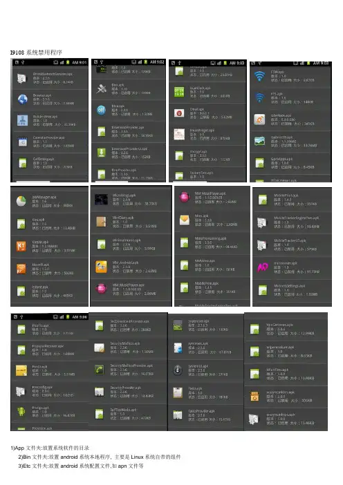
I9108系统禁用程序1)App文件夹:放置系统软件的目录2)Bin文件夹:放置android系统本地程序, 主要是Linux系统自带的组件3)Etc文件夹:放置android系统配置文件,如apn文件等4)Fonts文件夹:放置字体文件,包含标准字体和粗体、斜体、中文、英文等5)Framework文件夹:放置android系统平台框架文件及布局控制6)Lib文件夹:放置系统底层库及运行库文件7)Media文件夹:放置系统铃声音乐文件夹及开机动画文件8)Tts文件夹:放置手机的语音文件9)Usr文件夹: 放置用户文件,包含共享、键盘布局、时间区域文件等。
10)Vendor文件夹:放置ROM厂商定制内容11)Xbin文件夹:放置用户系统支持程序文件12)Build.prop文件:系统属性配置文件BackupAndRestore 备份程序(如果禁用的话不能备份和恢复,建议不禁用,之前的贴都是禁用的) DrmProvider.apk DRM数字版权提供(不用说,可以禁用)Email.apk 电子邮件客户端(如果有用可以不禁,可以禁用)GenieWidget.apk 天气与新闻(我觉得无用。
可以禁用)GoogleTranslate.apk 谷歌翻译(我觉得无用。
可以禁用)LiveWallpapersPicker.apk 动态壁纸(这个我没有禁用。
我怕用不了桌面,自己决定)Maps.apk 电子地图(对于占几M的内存,有其它导航可以代替,可以禁用) MarketUpdater.apk 谷歌市场升级(我觉得无用。
可以禁用)Mstore.apk 魅族商店(禁用用不了软件中心。
买的软件验证不了,自己决定)MusicOnline.apk 魅族在线音乐(我觉得无用。
可以禁用)MzInput.apk 魅族输入法(我用百度的,自己决定)NotePaper.apk 便签(自己决定)MzSimContacts.apk 魅族的SIM卡通讯录(我觉得无用。

MP15802A, 380 KHz Step-Down ConverterThe Future of Analog IC TechnologyTMTMDESCRIPTIONThe MP1580 is a monolithic step-down switchmode converter with a built in internal power MOSFET. It achieves 2A continuous output current over a wide input supply range with excellent load and line regulation.Current mode operation provides fast transient response and eases loop stabilization.Fault condition protection includes cycle-by-cycle current limiting and thermal shutdown. In shutdown mode the regulator draws 23µA of supply current.The MP1580 requires a minimum number of readily available standard external components. A synchronization pin allows the part to be driven to 600KHz.EVALUATION BOARD REFERENCEBoard NumberDimensions EV00072.3”X x 1.5”Y x 0.5”ZFEATURES• 2A Output Current• 0.18Ω Internal Power MOSFET Switch• Stable with Low ESR Output CeramicCapacitors• Up to 95% Efficiency • 23µA Shutdown Mode • Fixed 380KHz Frequency • Thermal Shutdown• Cycle-by-Cycle Over Current Protection • Wide 4.75 to 25V Operating Input Range • Output Adjustable from 1.22V to 21V • Programmable Under Voltage Lockout • Frequency Synchronization Input • Available in an 8-Pin SO PackageAPPLICATIONS• Distributed Power Systems • Battery Chargers• Pre-Regulator for Linear Regulators“MPS” and “The Future of Analog IC Technology” are Trademarks of Monolithic Power Systems, Inc.TYPICAL APPLICATIONC5E F F I C I E N C Y (%)OUTPUT CURRENT (A)MP1580_TAC_EC01Efficiency vsOutput Current VoltagePACKAGE REFERENCE* For Tape & Reel, add suffix –Z (eg. MP1580HS–Z) For Lead Free, add suffix –LF (eg. MP1580HS –LF–Z)**For Tape & Reel, add suffix –Z (eg. MP1580HP–Z) For Lead Free, add suffix –LF (eg. MP1580HP –LF–Z)ABSOLUTE MAXIMUM RATINGS (1) Supply Voltage (V IN) (27V)Switch Voltage (V SW)..................–1V to V IN + 1V Bootstrap Voltage (V BS).......................V SW + 6V Feedback Voltage (V FB).................–0.3V to +6V Enable/UVLO Voltage (V EN)...........–0.3V to +6V Comp Voltage (V COMP)...................–0.3V to +6V Sync Voltage (V SYNC)......................–0.3V to +6V Junction Temperature............................+150°C Lead Temperature.................................+260°C Storage Temperature..............–65°C to +150°C Recommended Operating Conditions (2) Input Voltage (V IN).........................4.75V to 25V Operating Temperature...............–40°C to +125°C Thermal Resistance (3)θJA θJCSOIC8....................................105.....50...°C/W PDIP8.....................................95......55...°C/W Notes:1) Exceeding these ratings may damage the device.2) The device is not guaranteed to function outside of itsoperating conditions.3) Measured on approximately 1” square of 1 oz copper.ELECTRICAL CHARACTERISTICSV IN = 12V, T A = +25°C, unless otherwise noted.Parameter Symbol ConditionMinTypMaxUnitsFeedback Voltage 4.75V ≤ V IN≤ 25VV COMP < 2V1.198 1.222 1.246 VUpper Switch-On Resistance 0.18 ΩLowerSwitch-OnResistance 10 ΩUpper Switch Leakage V EN = 0V, V SW = 0V 0 10 µACurrent Limit (4) 2.4 3.0 3.6 ACurrent Limit Gain.Output Current to Comp Pin Voltage1.95 A/VError Amplifier Voltage Gain 400 V/VError Amplifier Transconductance ∆I C = ±10µA 500 770 1100 µA/VOscillatorFrequency 342 380 418 KHzShort Circuit Frequency V FB = 0V 20 35 54 KHzSync Frequency Sync Drive 0V to 2.7V 445 600 KHzELECTRICAL CHARACTERISTICS (continued)V IN = 12V, T A = +25°C, unless otherwise noted.Parameter Symbol Condition Min Typ Max UnitsMaximum Duty CycleV FB = 1.0V 90 % Minimum Duty CycleV FB = 1.5V 0 % EN Shutdown Threshold Voltage I CC > 100µA 0.7 1.0 1.3 V Enable Pull-Up Current V EN = 0V 1.15 1.46 1.8 µA EN UVLO Threshold Rising V EN Rising 2.37 2.495 2.62 V EN UVLO Threshold Hysteresis210mVSupply Current (Shutdown) V EN ≤ 0.4V23 36 µA Supply Current (Quiescent) V EN ≥ 2.6V, V FB = 1.4V 1.0 1.2 mA Thermal Shutdown160°CNote:4) Derate current limit 0.011A/°C.PIN FUNCTIONSPin #NameDescription1 BSBootstrap (C5). This capacitor is needed to drive the power switch’s gate above thesupply voltage. It is connected between SW and BS pins to form a floating supply acrossthe power switch driver. The voltage across C5 is about 5V and is supplied by the internal +5V supply when the SW pin voltage is low.2 INSupply Voltage. The MP1580 operates from a +4.75V to +25V unregulated input. C1 isneeded to prevent large voltage spikes from appearing at the input.3 SW Switch. This connects the inductor to either IN through M1 or to GND through M2.4 GND Ground. This pin is the voltage reference for the regulated output voltage. For this reasoncare must be taken in its layout. This node should be placed outside of the D1 to C1ground path to prevent switching current spikes from inducing voltage noise into the part. 5 FBFeedback. An external resistor divider from the output to GND, tapped to the FB pin sets the output voltage. To prevent current limit run away during a short circuit fault conditionthe frequency foldback comparator lowers the oscillator frequency when the FB voltage is below 700mV.6 COMP Compensation. This node is the output of the transconductance error amplifier and theinput to the current comparator. Frequency compensation is done at this node byconnecting a series R-C to ground. See the compensation section for exact details.7 ENEnable/UVLO. A voltage greater than 2.62V enables operation. For complete low currentshutdown the EN pin voltage needs to be less than 700mV.8 SYNC Synchronization Input. This pin is used to synchronize the internal oscillator frequency toan external source. There is an internal 11k Ω pull down resistor to GND; therefore leaveSYNC unconnected if unused.OPERATIONThe MP1580 is a current mode regulator; the COMP pin voltage is proportional to the peak inductor current. At the beginning of a cycle: the upper transistor M1 is off; the lower transistor M2 is on (refer to Figure 1); the COMP pin voltage is higher than the current sense amplifier output and the current comparator’s output is low. The rising edge of the 380KHz CLK signal sets the RS Flip-Flop. Its output turns off M2 and turns on M1, thus connecting the SW pin and inductor to the input supply. The increasing inductor current is sensed and amplified by the Current Sense Amplifier. Ramp compensation is summed to Current Sense Amplifier output and compared to the Error Amplifier output by the Current Comparator. When the Current Sense Amplifier plus Slope Compensation signal exceeds the COMP pin voltage, the RS Flip-Flop is reset and theMP1580 reverts to its initial M1 off, M2 on, state. If the Current Sense Amplifier plus Slope Compensation signal does not exceed the COMP voltage, then the falling edge of the CLK resets the Flip-Flop.The output of the Error Amplifier integrates the voltage difference between the feedback and the 1.222V bandgap reference. The polarity is such that an FB pin voltage less than 1.222V increases the COMP pin voltage. Since the COMP pin voltage is proportional to the peak inductor current, an increase in its voltage increases the current delivered to the output. The lower 10Ω switch ensures that the bootstrap capacitor voltage is charged during light load conditions. An external Schottky Diode D1 carries the inductor current when M1 is off (see Figure 1).IN EN SYNC GNDSW BSFigure 1—Functional Block DiagramAPPLICATION INFORMATIONCOMPONENT SELECTIONSync Pin OperationThe SYNC pin driving waveform should be a square wave with a rise time less than 20ns. The Minimum High voltage level is 2.7V and the Low level is less than 0.8V. The frequency of the external sync signal needs to be greater than 445KHz.A rising edge on the SYNC pin forces a reset of the oscillator. The upper transistor M1 is switched off immediately if it is not already off. 250ns later M1 turns on connecting SW to V IN . Setting the Output VoltageThe output voltage is set using a resistive voltage divider from the output to FB (see Figure 3). The voltage divider divides the output voltage down by the ratio:2R 1R 2R V V OUTFB +=Where V FB is the feedback voltage and V OUT is the output voltage. Thus the output voltage is:2R 2R 1R 222.1V OUT +×= R2 can be as high as 100k Ω, but a typical value is 10k Ω. Using this value, R1 is determined by:)222.1V (18.81R OUT −×≅For example, for a 3.3V output voltage, R2 is 10k Ω and R1 is 17k Ω.InductorThe inductor is required to supply constant current to the output load while being driven by the switched input voltage. A larger value inductor results in less ripple current that in turn results in lower output ripple voltage.However, the larger value inductor has a larger physical size, higher series resistance and/or lower saturation current. Choose an inductor that does not saturate under the worst-case load conditions.A good rule for determining the inductance is to allow the peak-to-peak ripple current in the inductor to be approximately 30% of the maximum load current. Also, make sure that the peak inductor current (the load current plus half the peak-to-peak inductor ripple current) is below the 2.4A minimum current limit.The inductance value can be calculated by the equation:If V )V V (V L IN OUT IN OUT ∆××−×=Where V IN is the input voltage, f is the oscillator frequency and ∆I is the peak-to-peak inductor ripple current. Table 1 lists a number of suitable inductors from various manufacturers.Table 1—Inductor Selection GuidePackage Dimensions(mm)Vendor/ Model Core Type Core MaterialW L HSumidaCR75 Open Ferrite 7.0 7.8 5.5CDH74 Open Ferrite 7.3 8.0 5.2CDRH5D28Shielded Ferrite 5.5 5.7 5.5CDRH5D28Shielded Ferrite 5.5 5.7 5.5CDRH6D28Shielded Ferrite 6.7 6.7 3.0CDRH104R Shielded Ferrite 10.110.0 3.0Toko D53LCType AShielded Ferrite 5.0 5.0 3.0D75C Shielded Ferrite 7.6 7.6 5.1D104C Shielded Ferrite 10.010.0 4.3D10FL Open Ferrite 9.7 11.5 4.0CoilcraftDO3308 Open Ferrite 9.4 13.0 3.0DO3316 Open Ferrite 9.4 13.0 5.1Input CapacitorThe input current to the step-down converter is discontinuous, so a capacitor is required to supply the AC current to the step-down converter while maintaining the DC input voltage. A low ESR capacitor is required to keep the noise at the IC to a minimum. Ceramic capacitors are preferred, but tantalum or low-ESR electrolytic capacitors will also suffice.The input capacitor value should be greater than 10µF. The capacitor can be electrolytic, tantalum or ceramic. However, since it absorbs the input switching current it requires an adequate ripple current rating. Its RMS current rating should be greater than approximately 1/2 of the DC load current.To ensure stable operation, C1 should be placed as close to the IN pin as possible. Alternately, a smaller high quality ceramic 0.1µF capacitor may be placed closer to the IN pin and a larger capacitor placed further away. If using this technique, it is recommended that the larger capacitor be a tantalum or electrolytic type capacitor. All ceramic capacitors should be placed close to the MP1580.Output CapacitorThe output capacitor is required to maintain the DC output voltage. Low ESR capacitors are preferred to keep the output voltage ripple low. The characteristics of the output capacitor also affect the stability of the regulation control system. Ceramic, tantalum or low ESR electrolytic capacitors are recommended. In the case of ceramic capacitors, the impedance at the oscillator frequency is dominated by the capacitance, so the output voltage ripple is mostly independent of the ESR. The output voltage ripple is estimated to be:2LCIN RIPPLEff V 4.1V ⎟⎟⎠⎞⎜⎜⎝⎛××≅ Where V RIPPLE is the output ripple voltage, f LC isthe resonant frequency of the LC filter and f is the oscillator frequency.In the case of tantalum or low-ESR electrolytic capacitors, the ESR dominates the impedance at the oscillator frequency, therefore the output ripple is calculated as:ESR RIPPLE R I V ×∆≅Where V RIPPLE is the output voltage ripple and R ESR is the equivalent series resistance of the output capacitors.Output Rectifier DiodeThe output rectifier diode supplies the current to the inductor when the upper transistor M1 is off. To reduce losses due to the diode forward voltage and recovery times, use a Schottky rectifier.Table 2 provides the Schottky rectifier part numbers based on the maximum input voltage and current rating.Table 2—Schottky Rectifier Selection Guide2A Load Current V IN (Max)Part NumberVendor15V 30BQ015 4B220 1SK23 6 20VSR22 6 20BQ030 4 B230 1SK23 6 SR23 3, 6 26VSS23 2, 3Table 3 lists some rectifier manufacturers. Table 3—Schottky Diode ManufacturersVendor Web SiteDiodes, Inc.Fairchild Semiconductor General Semiconductor International Rectifier On Semiconductor Pan Jit International Choose a rectifier that has a maximum reverse voltage rating greater than the maximum input voltage, and a current rating greater than the maximum load current.CompensationThe system stability is controlled through the COMP pin. COMP is the output of the internal transconductance error amplifier. A series capacitor-resistor combination sets a pole-zero combination to control the characteristics of the control system. The DC loop gain is:OUTFBVEA CS LOAD VDC V V A G R A ×××= Where A VEA is the transconductance error amplifier voltage gain, 400 V/V, G CS is the current sense gain, (roughly the output current divided by the voltage at COMP), 1.95 A/V and R LOAD is the load resistance (V OUT / I OUT where I OUT is the output load current).The system has 2 poles of importance, one is due to the compensation capacitor (C3), and the other is due to the output capacitor (C2). These are:VEAEA1P A 3C 2G f ××π=Where P1 is the first pole and G EA is the error amplifier transconductance (770µA/V). andLOAD2P R 2C 21f ××π=The system has one zero of importance, due tothe compensation capacitor (C3) and the compensation resistor (R3). The zero is:3R 3C 21f 1Z ××π=If a large value capacitor (C2) with relatively high equivalent-series-resistance (ESR) is used, the zero due to the capacitance and ESR of the output capacitor can be compensated by a third pole set by R3 and C6. The pole is:3R 6C 21f 3P ××π=The system crossover frequency (the frequency where the loop gain drops to 1, or 0dB) is important. A good rule of thumb is to set the crossover frequency to approximately 1/10 of the switching frequency.In this case, the switching frequency is 380KHz, so use a crossover frequency, f C , of 40KHz. Lower crossover frequencies result in slower response and worse transient load recovery. Higher crossover frequencies can result in instability.Choosing the Compensation Components The values of the compensation components given in Table 4 yield a stable control loop for the output voltage and capacitor given. Table 4—Compensation Values for Typical Output Voltage/Capacitor CombinationsV OUT C2 R3 C3 C62.5V 22µF Ceramic 7.5k Ω 2.2nF None3.3V 22µF Ceramic 10k Ω 2nF None 5V 22µF Ceramic 15k Ω 1.2nF None 12V 22µF Ceramic 33k Ω 1nF None2.5V 560µF/6.3V(30m Ω ESR) 200k Ω 1nF 100pF3.3V 560µF/6.3V(30m Ω ESR) 200k Ω 1nF 82pF5V 470µF/10V(30m Ω ESR) 250k Ω 1nF 56pF12V 220µF/25V(30m Ω ESR)250k Ω 1nF 27pFTo optimize the compensation components for conditions not listed in Table 4, use the following procedure:Choose the compensation resistor to set the desired crossover frequency. Determine the value by the following equation:FBOUTCS EA C V V G G f 2C 23R ××××π=Putting in the known constants and setting the crossover frequency to the desired 40KHz:OUT 8V 2C 1037.13R ×××≈Choose the compensation capacitor to set the zero below ¼ of the crossover frequency. Determine the value by the following equation:3R V 2C 22.03C OUT××>Determine if the second compensation capacitor, C6, is required. It is required if the ESR zero of the output capacitor happens at less than four times the crossover frequency. Or:1f R 2C 8C ESR ≥×××πor1V R 3R 1034.7OUTESR5≥×××−If this is the case, add the second compensation capacitor. Determine the value by the equation:3R R 2C 6C )MAX (ESR ×=Where R ESR(MAX) is the maximum ESR of the output capacitor. For example: V OUT = 3.3VC2= 22µF Ceramic (ESR = 10m Ω)Ω=××××≈−k 9.9)3.3()1022()1037.1(3R 68Use the nearest standard value of 10k Ω.nF 6.110103.3)1022(22.03C 36=××××>−Use a standard value of 2nF014.0f R 2C 2C ESR =×××πwhich is less than 1, therefore no second compensation capacitor is required.Table 5—Recommended Components forStandard Output VoltagesV OUT R1 L1 Minimum1.22V 0Ω6.8µH 1.5V 2.32k Ω 6.8µH 1.8V 4.75k Ω 10µH 2.5V 10.5k Ω 10µH 3.3V 16.9k Ω 15µH 5.0V 30.9k Ω 22µHNegative Output VoltageThe MP1580 can be configured as a buck-boost regulator to supply negative output voltage.Because the GND pin of the IC is now connected to the negative output voltage, the maximum allowable input voltage is the IC input voltage rating (25V) minus the negative output voltage value. A typical application circuit is shown in Figure 3.External Bootstrap DiodeIt is recommended that an external bootstrap diode be added when the system has a 5V fixed input or the power supply generates a 5V output. This helps improve the efficiency of the regulator. The bootstrap diode can be a low cost one such as IN4148 or BAT54.10nFFigure 2—External Bootstrap DiodeThis diode is also recommended for high dutycycle operation (whenINOUTV V >65%) and high output voltage (V OUT >12V) applications.TYPICAL APPLICATION CIRCUITSC5Figure 3—Application Circuit for -5V SupplyC5MP1580_F04 Figure 4—MP1580 with Murata 22µF/10V Ceramic Output CapacitorPACKAGE INFORMATIONSOIC8NOTE:1) Control dimension is in inches. Dimension in bracket is millimeters.PDIP8NOTICE: The information in this document is subject to change without notice. Please contact MPS for current specifications. Users should warrant and guarantee that third party Intellectual Property rights are not infringed upon when integrating MPS products into any application. MPS will not assume any legal responsibility for any said applications.。

南粳9108
佚名
【期刊名称】《江苏农村经济:品牌农资》
【年(卷),期】2015(000)006
【摘要】1.审定编号:苏审稻2013062.适应范围:适宜江苏省苏中及宁镇扬丘陵地区种植。
3.产量水平及特征特性:2011~2012年参加江苏省区试,两年区试平均亩产644.2公斤,2011年较对照淮稻9号增产5.2%,增产达极显著水平,2012年较对照淮稻9号增产3.2%,较对照镇稻14增产0.1%;
【总页数】1页(P42-42)
【正文语种】中文
【中图分类】F326.11
【相关文献】
1.迟熟中粳南粳9108高产特征特性及种植表现 [J], 王晓东;刘晓霞;殷勤;王显
2.稻作方式对优质食味品种南粳9108的产量、品质及效益的影响 [J], 姚义; 温凯; 杨武广; 谢成林; 唐建鹏; 张明伟; 田洁
3.不同类型缓控释肥对水稻南粳9108氮素利用的影响 [J], 徐辰峰
4.机插方式和栽插密度对超级稻南粳9108生长和产量的影响 [J], 刘绍贵;邵在胜;苏伟;郭保卫;徐迅;严瑾;景有翠
5.穗发芽对南粳9108稻米品质的影响 [J], 钱松;王春歌;杨亚东;王春松;黄欢
因版权原因,仅展示原文概要,查看原文内容请购买。
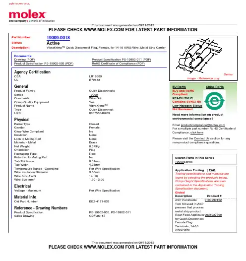
This document was generated on 09/11/2012PLEASE CHECK FOR LATEST PART INFORMATIONPart Number:19009-0018Status:ActiveDescription:VibraKrimp™ Quick Disconnect Flag, Female, for 14-16 AWG Wire, Metal Strip CarrierDocuments:Drawing (PDF)Product Specification PS-19902-011 (PDF)Product Specification PS-19902-005 (PDF)RoHS Certificate of Compliance (PDF)Agency CertificationCSA LR18689ULE79133GeneralProduct Family Quick Disconnects Series19009CommentsWire Grip Crimp Quality Equipment YesProduct Name VibraKrimp™Type Quick Disconnect UPC800755046939PhysicalBarrel Type Closed GenderFemale Glow-Wire Compliant No InsulationNone Lock to Mating Part None Material - Metal Brass Net Weight 0.679/g OrientationFlag Packaging TypeReel Polarized to Mating Part NoTab Thickness 0.81mm Tab Width4.75mmTemperature Range - Operating Per Wire Specification Wire Insulation Diameter 3.68mm Wire Size AWG 14, 16Wire Size mm²1.30 -2.00ElectricalVoltage - MaximumPer Wire Specification Material InfoOld Part NumberBBZ-4171-032Reference - Drawing NumbersProduct Specification PS-19902-005, PS-19902-011Sales DrawingCDFGS187Seriesimage - Reference onlyEU RoHSChina RoHSELV and RoHS Compliant REACH SVHCContains SVHC: No Low-Halogen Status Not ReviewedNeed more information on product environmental compliance?Email productcompliance@For a multiple part number RoHS Certificate of Compliance, click herePlease visit the Contact Us section for any non-product compliance questions.Search Parts in this Series 19009SeriesApplication Tooling | FAQTooling specifications and manuals are found by selecting the products below.Crimp Height Specifications are then contained in the Application Tooling Specification document.GlobalDescription Product #ASP Perishable Tool Kit used in ASP presses that process metal strip product0190290152Rear Feed Applicator for Quick Disconnect Female Flag Terminals, 14-16AWG Wire0638027700This document was generated on 09/11/2012PLEASE CHECK FOR LATEST PART INFORMATION/分销商库存信息: MOLEX 0190090018。