W981208BH中文资料
- 格式:pdf
- 大小:1.47 MB
- 文档页数:41
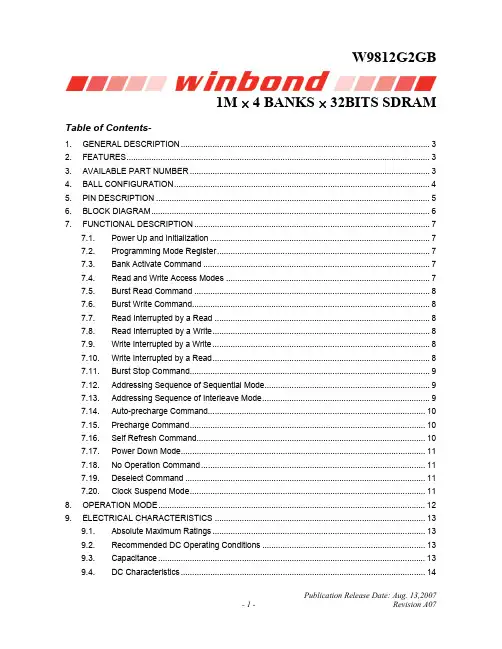
W981208BH4M × 4 BANKS × 8 BIT SDRAMPublication Release Date: October 2000- 1 - Revision A1GENERAL DESCRIPTIONW981208BH is a high-speed synchronous dynamic random access memory (SDRAM), organized as 4M words × 4 banks × 8 bits. Using pipelined architecture and 0.175 µm process technology, W981208BH delivers a data bandwidth of up to 143M words per second (-7). To fully comply with the personal computer industrial standard, W981208BH is sorted into three speed grades: -7, -75 and -8H. The -7 is compliant to the 143 MHz/CL3 or PC133/CL2 specification, the -75 is compliant to the PC133/CL3 specification, the -8H is compliant to the PC100/CL2 specificationAccesses to the SDRAM are burst oriented. Consecutive memory location in one page can be accessed at a burst length of 1, 2, 4, 8 or full page when a bank and row is selected by an ACTIVE command. Column addresses are automatically generated by the SDRAM internal counter in burst operation. Random column read is also possible by providing its address at each clock cycle. The multiple bank nature enables interleaving among internal banks to hide the precharging time.By having a programmable Mode Register, the system can change burst length, latency cycle, interleave or sequential burst to maximize its performance. W981208BH is ideal for main memory in high performance applications.FEATURES• 3.3V ±0.3V Power Supply • Up to 143 MHz Clock Frequency• 4,194,304 Words × 4 banks × 8 bits organization • Auto Refresh and Self Refresh • CAS Latency: 2 and 3• Burst Length: 1, 2, 4, 8, and full page • Burst Read, Single Writes Mode • Byte Data Controlled by DQM • Power-Down Mode• Auto-Precharge and Controlled Precharge • 4K Refresh cycles /64 mS • Interface: LVTTL• Packaged in TSOP II 54 pin, 400 mil - 0.80KEY PARAMETERSSYM.DESCRIPTIONMIN. /MAX.-7(PC133, CL2)-75(PC133, CL3)-8H (PC100)t CK Clock Cycle Time Min. 7 nS 7.5 nS 8 nS t AC Access Time from CLK Max. 5.4 nS 5.4 nS 6 nS t RP Precharge to Active Command Min. 15 nS 20 nS 20 nS t RCD Active to Read/Write Command Min. 15 nS 20 nS 20 nS I CC1 Operation Current (Single bank) Max. 80 mA 75 mA 70 mA I CC4 Burst Operation Current Max. 100 mA 95 mA 90 mA I CC6Self-refresh CurrentMax.2 mA2 mA2 mAW981208BH- 2 -PIN CONFIGURATIONW981208BHPublication Release Date: October 2000- 3 - Revision A1PIN DESCRIPTIONW981208BH- 4 -BLOCK DIAGRAMW981208BHPublication Release Date: October 2000- 5 - Revision A1ABSOLUTE MAXIMUM RATINGSPARAMETERSYMBOLRATINGUNITInput, Output Voltage V IN, V OUT -0.3 − V CC +0.3 V Power Supply Voltage V CC , V CCQ -0.3 − 4.6 VOperating Temperature T OPR 0 − 70 °C Storage Temperature T STG -55 − 150 °C Soldering Temperature (10s) T SOLDER 260 °CPower DissipationP D 1 W Short Circuit Output CurrentI OUT50mANote: Exposure to conditions beyond those listed under Absolute Maximum Ratings may adversely affect the life and reliabilityof the device.RECOMMENDED DC OPERATING CONDITIONS(Ta = 0 to 70°C)PARAMETER SYMBOL MIN. TYP. MAX. UNITPower Supply Voltage V CC 3.0 3.3 3.6 V Power Supply Voltage (for I/O Buffer)V CCQ 3.0 3.3 3.6 V Input High Voltage V IH 2.0 - V CC +0.3 V Input Low VoltageV IL-0.3-0.8VNote: V IH (max) = V CC / V CC Q+1.2V for pulse width < 5 nS V IL (min) = V SS / V SS Q-1.2V for pulse width < 5 nSCAPACITANCE(V CC = 3.3V, f = 1 MHz, T A = 25°C)Note: These parameters are periodically sampled and not 100% tested.W981208BH- 6 -AC CHARACTERISTICS AND OPERATING CONDITION(Vcc = 3.3V ± 0.3V, Ta = 0° to 70°C; Notes: 5, 6, 7, 8)PARAMETERSYM.-7(PC133, CL2)-75(PC133, CL3)-8H (PC100)UNITMIN.MAX.MIN.MAX.MIN.MAX.Ref/Active to Ref/Active Command Periodt RC 57 65 68 Active to precharge Command Periodt RAS 42 10000045 10000048 100000nS Active to Read/Write Command Delay Timet RCD 15 20 20 Read/Write(a) toRead/Write(b)Command Period t CCD 1 1 1 Cycle Precharge to Active Command Periodt RP 15 20 20 Active(a) to Active(b) Command Periodt RRD 15 15 20 Write Recovery Time CL* = 2 t WR 7.5 10 10CL* = 3 7 7.5 8 CLK Cycle Time CL* = 2 t CK7.5 1000 10 1000 10 1000CL* = 3710007.5100081000CLK High Level width t CH 2.5 2.5 3 CLK Low Level widtht CL2.52.53Access Time from CLKCL* = 2 t AC5.4 6 6CL* = 35.4 5.4 6 nS Output Data Hold Timet OH 3 3 3 Output Data High Impedance Time t HZ 3 7 3 7.5 3 8 Output Data Low Impedance Time t LZ 0 0 0 Power Down Mode Entry Time t SB 0 7 0 7.5 0 8 Transition Time of CLK (Rise and Fall) t T 0.5 10 0.5 10 0.5 10 Data-in Set-up Time t DS 1.5 1.5 2 Data-in Hold Time t DH 0.8 0.8 1 Address Set-up Time t AS 1.5 1.5 2 Address Hold Time t AH 0.8 0.8 1 CKE Set-up Time t CKS 1.5 1.5 2 CKE Hold Time t CKH 0.8 0.8 1 Command Set-up Time t CMS 1.5 1.5 2 Command Hold Time t CMH 0.8 0.8 1 Refresh Timet REF 64 64 64 mS Mode register Set Cycle Timet RSC141516nS*CL = CAS LatencyW981208BHPublication Release Date: October 2000- 7 - Revision A1DC CHARACTERISTICS(V CC = 3.3V ± 0.3V, T A = 0°− 70°C)PARAMETERSYMBOL MIN. MAX. UNIT NOTESInput Leakage Current(0V ≤ V IN ≤ V CC , all other pins not under test = 0V) I I(L)-55µAOutput Leakage Current(Output disable , 0V ≤ V OUT ≤ V CCQ ) I O(L)-55µALVTTL Output ″H ″ Level Voltage (I OUT = -2 mA )V OH2.4-VLVTTL Output ″L ″ Level Voltage (I OUT = 2 mA )V OL-0.4VW981208BH- 8 -Notes:1. Operation exceeds "ABSOLUTE MAXIMUM RATING" may cause permanent damage to the devices.2. All voltages are referenced to V SS3. These parameters depend on the cycle rate and listed values are measured at a cycle rate with the minimum values of t CK and t RC .4. These parameters depend on the output loading conditions. Specified values are obtained with output open.5. Power up sequence is further described in the "Functional Description" section.6. AC Testing ConditionsOutput Reference Level 1.4V/1.4V Output Load See diagram belowInput Signal Levels2.4V/0.4V Transition Time (Rise and Fall) of Input Signal2 nS Input Reference Level1.4V7. Transition times are measured between V IH and V IL .8. t HZ defines the time at which the outputs achieve the open circuit condition and is not referenced to output level.W981208BHPublication Release Date: October 2000- 9 - Revision A1OPERATION MODEFully synchronous operations are performed to latch the commands at the positive edges of CLK. Table 1 shows the truth table for the operation commands.Table 1 Truth Table (Note (1) , (2))Notes:(1) v = valid x = Don't care L = Low Level H = High Level (2) CKEn signal is input level when commands are provided.CKEn-1 signal is the input level one clock cycle before the command is issued. (3) These are state of bank designated by BS0, BS1 signals. (4) Device state is full page burst operation.(5) Power Down Mode can not be entered in the burst cycle.When this command asserts in the burst cycle, device state is clock suspend mode.W981208BH- 10 -FUNCTIONAL DESCRIPTIONPower Up and InitializationThe default power up state of the mode register is unspecified. The following power up and initialization sequence need to be followed to guarantee the device being preconditioned to each user specific needs.During power up, all Vcc and VccQ pins must be ramp up simultaneously to the specified voltage when the input signals are held in the "NOP" state. The power up voltage must not exceed Vcc +0.3V on any of the input pins or Vcc supplies. After power up, an initial pause of 200 µS is required followed by a precharge of all banks using the precharge command. To prevent data contention on the DQ bus during power up, it is required that the DQM and CKE pins be held high during the initial pause period. Once all banks have been precharged, the Mode Register Set Command must be issued to initialize the Mode Register. An additional eight Auto Refresh cycles (CBR) are also required before or after programming the Mode Register to ensure proper subsequent operation.Programming Mode RegisterAfter initial power up, the Mode Register Set Command must be issued for proper device operation. All banks must be in a precharged state and CKE must be high at least one cycle before the Mode Register Set Command can be issued. The Mode Register Set Command is activated by the low signals of RAS, CAS, CS and WE at the positive edge of the clock. The address input data during this cycle defines the parameters to be set as shown in the Mode Register Operation table. A new command may be issued following the mode register set command once a delay equal to t RSC has elapsed. Please refer to the next page for Mode Register Set Cycle and Operation Table.Bank Activate CommandThe Bank Activate command must be applied before any Read or Write operation can be executed. The operation is similar to RAS activate in EDO DRAM. The delay from when the Bank Activate command is applied to when the first read or write operation can begin must not be less than the RAS to CAS delay time (t RCD ). Once a bank has been activated it must be precharged before another Bank Activate command can be issued to the same bank. The minimum time interval between successive Bank Activate commands to the same bank is determined by the RAS cycle time of the device (t RC ). The minimum time interval between interleaved Bank Activate commands (Bank A to Bank B and vice versa) is the Bank to Bank delay time (t RRD ). The maximum time that each bank can be held active is specified as t RAS (max).Read and Write Access ModesAfter a bank has been activated , a read or write cycle can be followed. This is accomplished by setting RAS high and CAS low at the clock rising edge after minimum of t RCD delay. WE pin voltage level defines whether the access cycle is a read operation (WE high), or a write operation (WE low). The address inputs determine the starting column address.Reading or writing to a different row within an activated bank requires the bank be precharged and a new Bank Activate command be issued. When more than one bank is activated, interleaved bank Read or Write operations are possible. By using the programmed burst length and alternating the access and precharge operations between multiple banks, seamless data access operation among many different pages can be realized. Read or Write Commands can also be issued to the same bank or between active banks on every clock cycle.W981208BHPublication Release Date: October 2000- 11 - Revision A1Burst Read CommandThe Burst Read command is initiated by applying logic low level to CS and CAS while holding RAS and WE high at the rising edge of the clock. The address inputs determine the starting column address for the burst. The Mode Register sets type of burst (sequential or interleave) and the burst length (1, 2, 4, 8, full page) during the Mode Register Set Up cycle. Table 2 and 3 in the next page explain the address sequence of interleave mode and sequential mode.Burst Write CommandThe Burst Write command is initiated by applying logic low level to CS, CAS and WE while holding RAS high at the rising edge of the clock. The address inputs determine the starting column address. Data for the first burst write cycle must be applied on the DQ pins on the same clock cycle that the Write Command is issued. The remaining data inputs must be supplied on each subsequent rising clock edge until the burst length is completed. Data supplied to the DQ pins after burst finishes will be ignored.Read Interrupted by a ReadA Burst Read may be interrupted by another Read Command. When the previous burst is interrupted, the remaining addresses are overridden by the new read address with the full burst length. The data from the first Read Command continues to appear on the outputs until the CAS latency from the interrupting Read Command the is satisfied.Read Interrupted by a WriteTo interrupt a burst read with a Write Command, DQM may be needed to place the DQs (output drivers) in a high impedance state to avoid data contention on the DQ bus. If a Read Command will issue data on the first and second clocks cycles of the write operation, DQM is needed to insure the DQs are tri-stated. After that point the Write Command will have control of the DQ bus and DQM masking is no longer needed.Write Interrupted by a WriteA burst write may be interrupted before completion of the burst by another Write Command. When the previous burst is interrupted, the remaining addresses are overridden by the new address and data will be written into the device until the programmed burst length is satisfied.Write Interrupted by a ReadA Read Command will interrupt a burst write operation on the same clock cycle that the Read Command is activated. The DQs must be in the high impedance state at least one cycle before the new read data appears on the outputs to avoid data contention. When the Read Command is activated, any residual data from the burst write cycle will be ignored.Burst Stop CommandA Burst Stop Command may be used to terminate the existing burst operation but leave the bank open for future Read or Write Commands to the same page of the active bank, if the burst length is full page. Use of the Burst Stop Command during other burst length operations is illegal. The Burst Stop Command is defined by having RAS and CAS high with CS and WE low at the rising edge of the clock. The data DQs go to a high impedance state after a delay which is equal to the CAS Latency in a burstW981208BH- 12 -read cycle interrupted by Burst Stop. If a Burst Stop Command is issued during a full page burst write operation, then any residual data from the burst write cycle will be ignored.Addressing Sequence of Sequential ModeA column access is performed by increasing the address from the column address which is input to the device. The disturb address is varied by the Burst Length as shown in Table 2.Table 2 Address Sequence of Sequential ModeAddressing Sequence of Interleave ModeA column access is started in the input column address and is performed by inverting the address bit in the sequence shown in Table 3.Table 3 Address Sequence of Interleave ModeW981208BHPublication Release Date: October 2000- 13 - Revision A1Auto-Precharge CommandIf A10 is set to high when the Read or Write Command is issued, then the auto-precharge function is entered. During auto-precharge, a Read Command will execute as normal with the exception that the active bank will begin to precharge automatically before all burst read cycles have been completed. Regardless of burst length, it will begin a certain number of clocks prior to the end of the scheduled burst cycle. The number of clocks is determined by CAS latency.A Read or Write Command with auto-precharge can not be interrupted before the entire burst operation is completed. Therefore, use of a Read, Write, or Precharge Command is prohibited during a read or write cycle with auto-precharge. Once the precharge operation has started, the bank cannot be reactivated until the Precharge time (t RP ) has been satisfied. Issue of Auto-Precharge command is illegal if the burst is set to full page length. If A10 is high when a Write Command is issued, the Write with Auto-Precharge function is initiated. The SDRAM automatically enters the precharge operation one clock delay from the last burst write cycle. This delay is referred to as Write t W R . The bank undergoing auto-precharge can not be reactivated until t W R and t RP are satisfied. This is referred to as t DAL , Data-in to Active delay (t DAL = t W R + t RP ). When using the Auto-precharge Command, the interval between the Bank Activate Command and the beginning of the internal precharge operation must satisfy t RAS (min).Precharge CommandThe Precharge Command is used to precharge or close a bank that has been activated. The Precharge Command is entered when CS, RAS and WE are low and CAS is high at the rising edge of the clock. The Precharge Command can be used to precharge each bank separately or all banks simultaneously. Three address bits, A10, BS0, and BS1, are used to define which bank(s) is to be precharged when the command is issued. After the Precharge Command is issued, the precharged bank must be reactivated before a new read or write access can be executed. The delay between the Precharge Command and the Activate Command must be greater than or equal to the Precharge time (t RP ).Self Refresh CommandThe Self Refresh Command is defined by having CS, RAS, CAS and CKE held low with WE high at the rising edge of the clock. All banks must be idle prior to issuing the Self Refresh Command. Once the command is registered, CKE must be held low to keep the device in Self Refresh mode. When the SDRAM has entered Self Refresh mode all of the external control signals, except CKE, are disabled. The clock is internally disabled during Self Refresh Operation to save power. The device will exit Self Refresh operation after CKE is returned high. A minimum delay time is required when the device exits Self Refresh Operation and before the next command can be issued. This delay is equal to the t AC cycle time plus the Self Refresh exit time.If, during normal operation, AUTO REFRESH cycles are issued in bursts (as opposed to being evenly distributed), a burst of 4,096 AUTO REFRESH cycles should be completed just prior to entering and just after exiting the self refresh mode.Power Down ModeThe Power Down mode is initiated by holding CKE low. All of the receiver circuits except CKE are gated off to reduce the power. The Power Down mode does not perform any refresh operations, therefore the device can not remain in Power Down mode longer than the Refresh period (t REF ) of the device.W981208BH- 14 -The Power Down mode is exited by bringing CKE high. When CKE goes high, a No Operation Command is required on the next rising clock edge, depending on t CK . The input buffers need to be enabled with CKE held high for a period equal to t CKS (min) + t CK (min).No Operation CommandThe No Operation Command should be used in cases when the SDRAM is in a idle or a wait state to prevent the SDRAM from registering any unwanted commands between operations. A No Operation Command is registered when CS is low with RAS, CAS, and WE held high at the rising edge of the clock. A No Operation Command will not terminate a previous operation that is still executing, such as a burst read or write cycle.Deselect CommandThe Deselect Command performs the same function as a No Operation Command. Deselect Command occurs when CS is brought high, the RAS, CAS, and WE signals become don't cares.Clock Suspend ModeDuring normal access mode, CKE must be held high enabling the clock. When CKE is registered low while at least one of the banks is active, Clock Suspend Mode is entered. The Clock Suspend mode deactivates the internal clock and suspends any clocked operation that was currently being executed. There is a one clock delay between the registration of CKE low and the time at which the SDRAM operation suspends. While in Clock Suspend mode, the SDRAM ignores any new commands that are issued. The Clock Suspend mode is exited by bringing CKE high. There is a one clock cycle delay from when CKE returns high to when Clock Suspend mode is exited.W981208BHPublication Release Date: October 2000- 15 - Revision A1TIMING WAVEFORMSCommand Input TimingW981208BH- 16 -Timing Waveforms, continuedRead TimingW981208BHPublication Release Date: October 2000- 17 - Revision A1Timing Waveforms, continuedControl Timing of Input /Output DataW981208BH- 18 -Timing Waveforms, continuedMode Register Set CycleW981208BHPublication Release Date: October 2000- 19 - Revision A1OPERATING TIMING EXAMPLEInterleaved Bank Read (Burst Length = 4, CAS Latency = 3)t RCt RASt RPt RASt RCD t RCDt RRDRAaRBdW981208BH- 20 -Operating Timing Example, continuedInterleaved Bank Read (Burst Length = 4, CAS Latency = 3, Autoprecharge)(CLK = 100 MHz)t RCt RASt RPt RPt RCDt RRD t RRDW981208BHPublication Release Date: October 2000- 21 - Revision A1Operating Timing Example, continuedInterleaved Bank Read (Burst Length = 8, CAS Latency = 3)t RRDW981208BH- 22 -Operating Timing Example, continuedInterleaved Bank Read (Burst Length = 8, CAS Latency = 3, Autoprecharge)W981208BHPublication Release Date: October 2000- 23 - Revision A1Operating Timing Example, continuedInterleaved Bank Write (Burst Length = 8)RRDW981208BH- 24 -Operating Timing Example, continuedInterleaved Bank Write (Burst Length = 8, Autoprecharge)W981208BHPublication Release Date: October 2000- 25 - Revision A1Operating Timing Example, continuedPage Mode Read (Burst Length = 4, CAS Latency = 3)W981208BH- 26 -Operating Timing Example, continuedPage Mode Read /Write (Burst Length = 8, CAS Latency = 3)W981208BHPublication Release Date: October 2000- 27 - Revision A1Operating Timing Example, continuedAuto Precharge Read (Burst Length = 4, CAS Latency = 3)(CLK = 100 MHz)CLKDQCKEDQMA0-A9,A11A10BS1WECASRASCSBS0t RCt RCDW981208BH- 28 -Operating Timing Example, continuedAuto Precharge Write (Burst Length = 4)t RCt RP t RPW981208BHPublication Release Date: October 2000- 29 - Revision A1Operating Timing Example, continuedAuto Refresh Cycle(CLK = 100 MHz)All Banks Prechage Auto RefreshAuto Refresh (Arbitrary Cycle)t RC t RCW981208BH- 30 -Operating Timing Example, continuedSelf Refresh Cyclet SBW981208BHPublication Release Date: October 2000- 31 - Revision A1Operating Timing Example, continuedBurst Read and Single Write (Burst Length = 4, CAS Latency = 3)t RCDW981208BH- 32 -Operating Timing Example, continuedPowerDown Modet SBNOPW981208BHPublication Release Date: October 2000- 33 - Revision A1Operating Timing Example, continuedAutoprecharge Timing (Read Cycle)APAPActActQ0Q6Q7t RPW981208BH- 34 -Operating Timing Example, continuedAutoprecharge Timing (Write Cycle)D1D3D7(1) CAS Latency=2When the Auto precharge command is asserted, the period from Bank Activate command to the start of internal precgarging must be at least tRAS (min).represents the Write with Auto precharge command.represents the start of internal precharging.represents the Bank Activate command.Note )W981208BHPublication Release Date: October 2000- 35 - Revision A1Operating Timing Example, continuedTiming Chart of Read to Write CycleTiming Chart of Write to Read CycleW981208BH- 36 -Operating Timing Example, continuedTiming Chart of Burst Stop Cycle (Burst Stop Command)Timing Chart of Burst Stop Cycle (Precharge Command)PRCGW981208BHPublication Release Date: October 2000- 37 - Revision A1Operating Timing Example, continuedCKE/DQM Input Timing (Write Cycle)W981208BH- 38 -Operating Timing Example, continuedCKE/DQM Input Timing (Read Cycle)W981208BHPublication Release Date: October 2000- 39 - Revision A1Operating Timing Example, continuedSelf Refresh/Power Down Mode Exit TimingW981208BH- 40 -PACKAGE DIMENSION54L TSOP (II)-400 milW981208BHPublication Release Date: October 2000 - 41 - Revision A1No. 4, Creation Rd. III,/11F, No. 115, Sec. 3, MinUnit 9Winbond Memory Lab.TEL: 408HeadquartersScience -Based Industrial Park,Hsinchu, TaiwanTEL: 886-3-5770066FAX: 886-3-5796096Voice & Fax -on -demand: 886-2-27197006Taipei Office-Sheng East Rd.,Taipei, TaiwanTEL: 886-2-27190505FAX: 886-2-27197502 Winbond Electronics (H.K.) Ltd.-15, 22F, Millennium City, No. 378 Kwun Tong Rd; Kowloon, Hong Kong TEL: 852-********FAX: 852-********Winbond Electronics North America Corp.Winbond Microelectronics Corp.Winbond Systems Lab.2727 N. First Street, San Jose,CA 95134, U.S.A.-9436666FAX: 408-5441798Note: All data and specifications are subject to change withou t notice.。