ED020OC1 Ver 0.4_20130402
- 格式:pdf
- 大小:849.90 KB
- 文档页数:39

牧马人的epon设备(插拔光纤时onu认证的报文)1、扩展发现OAMsend OAM:pkt len = 50, port = 0============================================================================== 00194264: 01 80 c2 00 00 02 00 1a ec 01 03 39 88 09 03 00 ; ...........9.... 00194274: 50 00 01 10 01 00 00 00 0e 05 ee 00 13 25 00 00 ; P............%.. 00194284: 00 00 02 10 01 00 00 00 0f 05 ee 00 13 25 00 00 ; .............%.. 00194294: 00 00 ; ................[000019ef:IGMP:0] mc tmr heartbeat[000019ef:APP:5] LOOPDETECT_TIMER_EXPIRED:port(255)[000019ef:APP:5] open port 1 period time out[000019ef:APP:3] vlan flooding ,dport 1, vlan count 0[000019ef:APP:5] open port 2 period time out[000019ef:APP:3] vlan flooding ,dport 2, vlan count 0[000019ef:APP:5] open port 3 period time out[000019ef:APP:3] vlan flooding ,dport 3, vlan count 0[000019ef:APP:5] open port 4 period time out[000019ef:APP:3] vlan flooding ,dport 4, vlan count 0[00001a0d:PTP:1] The tod_info is: $GPZDA001964000119700019.[00001a0d:PTP:0] update sys time 64633442256[00001a0d:PTP:4] trigger 1pps signal at time 65000000000(0xd224d4a0) [00001a0d:PTP:4] trigger tod info at time 65001000000(0xd225c8c4) Rcv OAM:pkt len = 60, port = 0============================================================================== 0014f068: 01 80 c2 00 00 02 00 e0 8e 88 01 00 88 09 03 00 ; ................ 0014f078: 50 00 01 10 01 00 00 00 0f 05 ee 00 13 25 00 00 ; P............%.. 0014f088: 00 00 02 10 01 00 00 00 0e 05 ee 00 13 25 00 00 ; .............%.. 0014f098:00 00 fe 07 11 11 11 01 21 00 00 00 ; ........!.......oam_ctc_build_pdu_infoLength=7+4x 07是最小值0x01:支持OAM扩展0x00:不支持OAM扩展ONU支持电信的版本号send OAM:pkt len = 57, port = 0==============================================================================001941d4: 01 80 c2 00 00 02 00 1a ec 01 03 39 88 09 03 00 ; ...........9....001941e4: 50 00 01 10 01 00 00 00 0e 05 ee 00 13 25 00 00 ; P............%..001941f4: 00 00 02 10 01 00 00 00 0f 05 ee 00 13 25 00 00 ; .............%.. 00194204: 00 00 fe 07 11 11 11 01 21 ; ........!.......[00001a33:APP:3] app_pkt_rx len 64 type 10 port 0[00001a37:OAM:0] oam_ind_oampdu(2、扩展的组织特定(Organization Specific)OAMPDU消息概述2.1 扩展的组织特定(Organization Specific)OAMPDU消息结构及定义扩展的组织特定OAMPDU消息(即Organization Specific OAMPDU)应符合IEEE 802.3-2008 Clause57.4.3.6中关于OAM扩展的规定。
实验6 – HW/SW 系统调试Targeting MicroBlaze™ on the Spartan-3E Starter KitHW/SW系统调试实验: MicroBlaze实验说明本实验将引导你完成处理器系统的调试。
将用到 XPS和 ChipScope实现系统软硬件的可视化。
实验目的通过实验,你将学会以下知识:∙想系统中添加 ChipScope分析器∙使用 Chipscope 分析器和SDK 调试器联合调试实验过程图1. MicroBlaze 系统打开工程步骤 1总体实验流程图:在 c :\xup\embedded\microblaze\labs\.路径下创建 lab6文件夹。
如果想继续前面的设计,你可以从lab5文件夹中复制其中的内容到lab6文件夹。
启动 Xilinx Platform Studio (XPS),打开工程,路径为c:\xup\embedded\microblaze\labs\lab6.❶在 c:\xup\embedded\microblaze\labs 路径下创建lab6 文件夹。
如果想继续实验5的设计,可以复制 lab5 中的内容到 lab6 。
❷ 点击 Start → Programs → Xilinx Platform Studio 8.2i → Xilinx Platform Studio ,打开XPS❸ 选择 Open Recent Project ,点击 OK ,浏览到C:\xup\embedded\microblaze\labs\lab6❹ 点击 system.xmp 打开工程。
ChipScope 核实例化步骤 2从IP 目录中添加 ChipScope 核到设计中,配置芯片和设计到下列端口,如图 6-2所示。
当OPB 地址,数据,控制总线上为一定的值时触发触发器。
Step 2: Instantiate Chipscope CoresStep 3: SDK and ChipscopeOperationStep 4: HW/SW DebugStep 1: Opening the ProjectStep 3:SDK and Chipscope OperationStep 4: HW/SW Debug图 6-2. ChipScope 核的连接❶从IP目录中的调试部分添加chipscope_icon 和 chipscope_opb_iba外设,并连接chipscope_opb_iba到OPB总线。
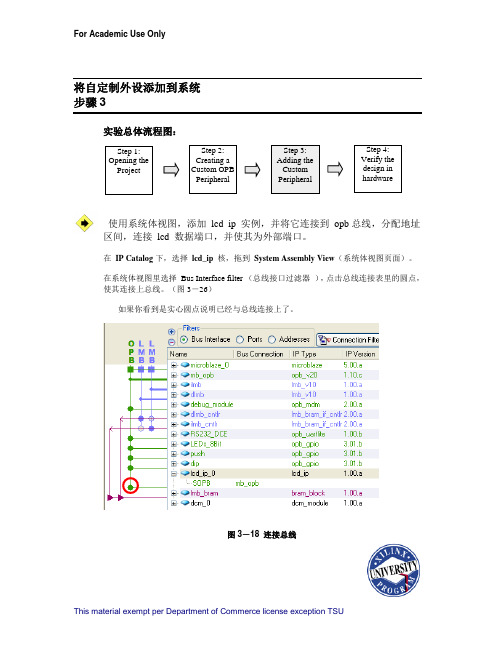
For Academic Use OnlyThis material exempt per Department of Commerce license exception TSU将自定制外设添加到系统 步骤3实验总体流程图:使用系统体视图,添加 lcd_ip 实例,并将它连接到 opb 总线,分配地址区间,连接lcd 数据端口,并使其为外部端口。
在IP Catalog 下,选择 lcd_ip 核,拖到 System Assembly View (系统体视图页面)。
在系统体视图里选择 Bus Interface filter (总线接口过滤器 ),点击总线连接表里的圆点,使其连接上总线。
(图3-26)如果你看到是实心圆点说明已经与总线连接上了。
图3-18 连接总线Step 1: Opening the ProjectStep 2: Creating a Custom OPB PeripheralStep 4: Verify the design in hardware选择Ports filter(端口过滤器),点击lcd_ip_0实例上的加号,点击网格中的下拉对话框,选择lcd_ip_0_lcd作为网络的名称(图3-27)。
图3-27 lcd_0实例赋值点击相同的位置,选择Make External 使它也成为外部端口。
选择Addresses filter(地址过滤器)除了lcd_ip_0 实例以外,其它的芯片的地址都已经锁定,点击Generate Addresses图标。
更改lcd外设的地址空间到32K你将会看到如下图所示(图3-28).图3-19 生成地址更改system.ucf文件,分配lcd连接。
从工程中移除lab2.c文件,添加C:¥xup¥embedded ¥labsolutions 文件夹中的lab3.c。
编译源代码,并重新烧入新的可执行文件。
保存工程,关闭XPS。
Epec 2024 Control ModuleTechnical DocumentDocument: 2024G08Updated: 1.10.2008Epec Oy reserves all rights for improvements without prior noticeDOCUMENT VERSION HISTORYDate Notes1.10.2008Document and layout updated 16.8.2006First released versionEpec Oy reserves all rights for improvements without prior noticeTABLE OF CONTENTS1 GENERAL (4)1.1 Purpose of This Document (4)1.2 About Manufacturer (4)1.3 Epec CAN Module Family (4)1.4 Basic skills required (4)1.5 Safety guidelines (4)1.6 Warranty (5)1.7 Limited liability (6)1.8 Environmental statement (6)2 I/O MODULE GENERAL DESCRIPTION (7)2.1 Programming Environment (7)2.1.1 Codesys 2.1 (7)2.1.2 Codesys 2.3 (8)2.2 CANopen Indexes (8)3 INPUT / OUTPUT SPECIFICATIONS (9)3.1 Configurable I/Os (9)3.2 Digital Input (10)3.3 Current Measuring Feedback (11)3.4 Digital Input / PWM Output / Digital Output (12)3.5 Digital Input / Analog Input (15)3.6 Digital Input / Digital Output (sinking) (17)3.7 Digital Input / Pulse Input (19)3.8 Specification for Internal Diagnostics (21)3.9 Closed Loops Wiring (21)3.10 I/O / IEC Map (22)3.11 AMPSEAL Connectors (23)3.12 AMPSEAL Cable Dimensions (23)4 POWER SUPPLY (24)4.1 Overvoltage Protection (24)4.2 Power Consumption (24)4.3 Power Supply Pins (24)5 BUS CONNECTION (25)5.1 Bus Connection Pins (25)5.2 CAN Interface (25)6 ENVIRONMENTAL CHARACTERS (26)6.1 Protection (26)6.2 EMC Tests (26)6.3 Environmental Tests (30)7 HOUSING (32)7.1 Mounting (32)7.2 Unit Dimensions (33)8ADDITIONAL DOCUMENTS (34)Epec Oy reserves all rights for improvements without prior notice1 GENERAL1.1 Purpose of This DocumentThis technical document is meant to be used in system development. This document containsnecessary data concerning the module in question, which system designer needs in systemdevelopment work.Copying of this document without permission is prohibited. All trademarks mentioned in thisdocument are owned by their manufacturers.1.2 About ManufacturerEpec Oy helps its customers to manufacture efficient, safe and environmental friendly mobileworking machines and special vehicles which help their customers to maximise theirproductivity.Epec is a solution provider specialized in embedded control systems, vehicle computers andinformation logistics systems for mobile machines. We believe that we know control systems forchallenging conditions and we are able to offer a total solution from control units to projectservices and designing.1.3 Epec CAN Module FamilyEpec CAN Module Family is designed to operate in extreme environments, where vibration,wide temperature changes and moisture are normal conditions. The requirements for thesystem’s reliability and safety have been the key words in module family development. A smalland protective module casing keeps inside high performance microcontroller with lots of controlcapabilities.1.4 Basic skills requiredThe user of this document must have professional skills on machine controlling, CANcommunication, PLCopen programming according to IEC61131-1 and should have skills to useCoDeSys 2.1/2.3 programming environment.Please refer CoDeSys 2.1/2.3 manual for further information on programming environment andrequired installations.Please refer CAN and CANopen documentation from CAN in Automation (CiA) for furtherinformation on communication issues.1.5 Safety guidelinesThe user of this documentation should follow general machine safety guidelines, directives andregulation appropriate to his/her country or market area.This product does not comply with SIL2 or SIL3 classifications and should not be used in suchapplications, e.g. lifting people, where SIL 2 or SIL3 are required by directives or otherregulations.A separate safety analysis is always recommended for the machine and its control system. Thefeatures of this product should be well documented in machine and control system documentsEpec Oy reserves all rights for improvements without prior noticeso that the machine operator has the right information how to operate the machine correctly andsafely.This product is designed to be used only for machine controlling purposes. The manufacturerdoes not assume any responsibility for this product being fit for any particular application, unlessotherwise expressly stated in writing by the manufacturer.This product complies with those certifications and standards that are listed below. Themanufacturer does not guarantee that this product complies any other certification, standard ortest than listed below.This product is not field serviceable, so it should not be opened at any situation.An external fuse should be installed for the product or the system power supply.The system should be designed and constructed according to the Epec general mounting andcabling instruction document.Epec Oy reserves a right to improve its products without a further notice.1.6 WarrantyThe manufacturer does not assume any responsibility for the products being fit for any particularpurpose, unless otherwise expressly stated in writing by the manufacturer.The manufacturer gives the warranty of twelve (12) months to the products and thereto relatedfirmware from commissioning or eighteen (18) months from the date of delivery of the productswhich ever occurs firstThe manufacturer is during the warranty period responsible for defects in the products andthereto related firmware resulting from faults in material, design or workmanship. Themanufacturer’s only obligation under this warranty is to, at its sole discretion, either to replacethe products and/or thereto related firmware or to repair the defective products. Themanufacturer shall, at its sole option, repair the products at its manufactory in Seinäjoki,Finland.The warranty does not cover any costs related to removing or fastening of devices related to theproducts. Neither does the warranty cover the expenses of sending devices to or from themanufacturer for repairs. The warranty does not cover possible expenses relating to travelling,accommodation, daily benefits, etc. of installers.The warranty becomes null and void if the buyer and/or a third party alters the products or thefirmware in any way or if they are not used in accordance with the Manufacturer’s operatinginstructions.All claims with respect to defects in the products shall be made to the manufacturer withoutdelay and no later than on the seventh (7th) day after the defect has been or should have beendiscovered by the buyer. The manufacturer strives to reply to the claim in writing within two (2)weeks from the receipt of the claim. The buyer shall attach to the claim a possible error report orequivalent explanation of the grounds for the claim.The manufacturer gives no other warranties whatsoever for the products than the warranty setout in this section and thus the warranty given in this section sets forth the warranty given by themanufacturer in its entirety.Epec Oy reserves all rights for improvements without prior notice1.7 Limited liabilityThe manufacturer shall under no circumstances be liable for loss of production, loss of profit,loss of use or any other consequential damages and/or indirect losses, whatever their causemay be. In case claims based on product liability are brought against the Manufacturer for whichclaims the manufacturer may be liable, the manufacturer’s liability is limited to the extentnormally covered under normal product liability insurances.The buyer shall compensate the manufacturer to the extent that the manufacturer might beliable to pay damages as a result of claims based on product liability according to paragraphabove.1.8 Environmental statementThe manufacturer uses ISO14001 environmental certified processes and materials tomanufacture products. The manufacturer undertakes to arrange for the recycling and scrappingof the products that are returned to the manufacturer by the buyer and/or the products that arereceived by the Manufacturer in connection with maintenance services performed as a result ofthat repairing of the products is deemed by the manufacturer to be inappropriate.The manufacturer will charge a scrapping fee from the buyer according to the manufacturer'sprice list in force from time to time. No scrapping fee will, however, be charged for products thatare received by the manufacturer during the warranty period.Epec Oy reserves all rights for improvements without prior notice2 I/O MODULE GENERAL DESCRIPTIONI/O Module is part of the Epec CAN Module Family. I/O Module has large amount of digital andanalog inputs and digital outputs. Digital outputs can be configured to be used as digital inputs and vice versa. Module is used in a CAN control module system as a multifunction controller with different kinds of sensors and actuators, such as proportional valves, servo motors, andelectro-hydraulic components. This PLCopen programmable (with CoDeSys tool) module canalso be used as an independent controller because of digital and analog I/O capabilities. I/OModule has two CAN-busses.FeaturesApplications • ISO High Speed CAN1 interface• ISO High Speed CAN2 interface• Operating voltage 10 - 30 VDC• Recommended operating voltage 24 VDC• Overvoltage protection• Overheating protection• Short-circuit protection for outputs• Gold plated, locked and sealed connectors:8-pin AMPSEAL for module connection3 x 23-pin AMPSEAL for I/O• Small outline dimensions: 147 x 113 x 46• Weight 0,7 kg• Forest Machines • Road Maintenance • Construction Machines • Crushing Stations • Industrial Machines • Agricultural applications • Automation applications • Mining MachinesMonitoring FunctionsFollowing issues can be monitored by the application• Supply voltage• Firmware/application code corruption• Module temperatureSoftware deadlock is monitored by the hardware watchdog that reboots the moduleautomatically after 300 ms software deadlock.2.1 Programming EnvironmentThis product can be programmed with either CoDeSys 2.1 or CoDeSys 2.3 depending on themodule’s firmware. If the firmware’s runtime is older than 2.1x, the programming environment isCoDeSys 2.1 and if the runtime is 2.3.x or newer the programming environment is CoDeSys2.3.The runtime version can be checked from index with a CANopen tool, for example withCANmoon.2.1.1 Codesys 2.1• Flash• 248 x 16-bit flash saved parameters (Runtime older than 2.15)• 756 x 16-bit flash saved parameters (Runtime 2.15 or newer)• CAN buses• Supported baud rates 20, 50, 100, 125, 250, 500 and 1000 kbit/s.• CAN1• CANopen• CAN2• User programmable• J1939Epec Oy reserves all rights for improvements without prior notice• Pulse inputs• Maximum pulse input frequency 20 kHz.• Joint frequency for all pulse inputs. (e.g. four channel in use --> 5 kHz for each channel.)• Minimum PWM frequency• 40 Hz for 20 MHz module• 80 Hz for 40 MHz module2.1.2 Codesys 2.3• Flash• 6200 bytes flash saved parameters.• 10 separately saved sets.• Maximum code size 254 kb.• CAN-buses• User programmable CAN for all physical CAN-buses• Supported baud rates 50, 100, 125, 250, 500 and 1000 kbit/s.• Supported protocols• CANopen (for all physical buses)• J1939 (only for one bus in the same module)• ISOBUS (only for one bus in the same module)• Possible to add external c-programmed library• Minimum PWM frequency• 40 Hz for 20 MHz module• 80 Hz for 40 MHz module• Maximum pulse input frequency 40 kHz. Joint frequency for all pulse inputs. (e.g. fourchannel in use --> 10 kHz for each channel). Is dependable for the other interrupt load inmodule (for example heavy CAN-traffic can reduce maximum frequency).2.2 CANopen IndexesCANopen communication features can be installed through software, for example NodeIDs andCAN rates. For more information refer to programming manuals.Epec Oy reserves all rights for improvements without prior notice3 INPUT / OUTPUT SPECIFICATIONSI/O module contains inputs and outputs or, in other words, I/O pins of many different types.There are, for example, outputs which source current and outputs which sink current.Furthermore, there are I/O pins which can be used as inputs or as outputs at the control of theapplication programmer.3.1 Configurable I/Os DI AI PI DO PWMMax Amount Digital Input Analog Input Current Measuring Feedback Pulse Input Digital Output (sourcing) Digital Output (sinking) Pulse Width Modulation Output4 x4 x24 x x x8 x x4 x x8 x x52 48 12 8 28 24The usage of each I/O pin is determined by the application.Epec Oy reserves all rights for improvements without prior notice3.2 Digital InputPins X1.19, X1.20, X2.19, and X2.20 are ground referenced inputs (DI ).Pins are associated with a bit variable in the IX area in PLCopen programming environment.The application program will see there a logical zero when the pin is grounded or left open anda logical one when the pin is connected to a positive voltage source.Electrical Characteristics Symbol Parameter ConditionsMin Max Units V I Greater than 4,3 V (Note 1)9,0 11 k Ω R I Input Resistance Referenced to 1,3 V;V I Less than 4,3 V (Note 1)6,2 7,6 k Ω V IH Input High Voltage4,8 30 V V IL Input Low Voltage-0,5 4,2 V t C=10 ms (Note 2, 3, 4, 5) 12 Hz f I Input Frequency Variable t C (Note 2, 3, 5)1/8t CC I Input Capacitance 37 57 nFNote 1: With input voltages below 4,3 V it seems like the internal input resistance wasconnected to a 1,3 V voltage source.Note 2: t C denotes software cycle time.Note 3: Violating this rating may lead to system not recognizing all input state transitions.Note 4: These parameters depend on software cycle time.Note 5: Applies to inputs used as normal digital input. Violating this rating may lead toapplication program not noticing all input state transitions.Connection PrincipleEpec Oy reserves all rights for improvements without prior notice3.3 Current Measuring FeedbackPins X1.5, X1.6, X2.3, and X2.4 are normally used as a return path for the loads of PWM outputs. These kinds of pins have a small shunt resistor connected to ground. The shunt resistor is used to measure the current flowing through the load. Nothing prevents using these pins to measure currents from other sources as well.In PLCopen programming environment, there is a word variable in IW area associated with each pin from where the software can read the actual current flowing into the pin.Electrical Characteristics Symbol Parameter ConditionsMin Max Units R I Input Resistance0,21 0,23 Ω Analog measuring range 0,0 1,0 A I I Input Current (Note 1) 1,7 A TIRETotal Input Referred Error55mANote 1: Exceeding the max value might cause damage to input.Connection PrincipleA pin where the upper wire of the load is connected is PWM output / digital output. This illustrates the normal way to connect loads when load current measurement is desired.Epec Oy reserves all rights for improvements without prior notice3.4 Digital Input / PWM Output / Digital OutputThese pins are current sourcing outputs. In other words, pin connects the load to positive supply voltage. The application program can also simultaneously monitor the actual state of the pin. This feature makes it possible to detect short circuits to the ground. Open loads can not be detected because the internal load resistor is connected to the ground.Connector X1 Connector X2X1.1 X1.2 X1.3 X1.4 X1.7 X1.8 X1.14 X1.15 X1.16 X1.17 X1.22 X1.23 X2.1 X2.2 X2.5 X2.6 X2.7 X2.8 X2.9 X2.10 X2.16 X2.17 X2.22 X2.23These kind of outputs are also capable to generate pulse width modulated (PWM) output signals. This feature is useful when driving proportionally controlled loads, e.g. proportional hydraulic valves. Monitoring the state of the pin is generally not possible when the pin is used as a PWM signal output.PWM frequencies can be configured under software control in groups of outputs. The frequency is set by HW_SET_PWM_FREQ function call. The setting is done by a PWM channel but setting the frequency of one channel sets also the frequencies of all the other channels in the same groups.In very carefully selected applications a pin of this type can also be used as an input by using the output state monitoring feature. In those cases, the output functionality of the pin must of course be kept in off state. It must be taken care in system design that the output unintentionally switching to on state causes no harm to the system.Epec Oy reserves all rights for improvements without prior noticePWM Frequency Control Groups (PFCG)Group Channel Output pin 0 X1.231 X1.22 2 X1.173 X1.164 X1.15 X1.26 X1.47 X1.38 X2.29 X2.1 10 X2.9 A 11 X2.10B 12 X2.8C 13 X2.7D 14 X2.6E 15 X2.5 16 X1.717 X1.8 18 X1.15 19 X1.14 20 X2.17 21 X2.16 22 X2.22 F 23 X2.23Electrical Characteristics Symbol Parameter Conditions Min Max Units R O Output Resistance Output On 0,2 Ω I O Output Current Output On 3 A f PWM PWM Frequency (Note 1)40 2550 Hz Group A and F (Note 1) 2,5 MHz/ f PWM Group B, C, D and E (Note 1)312,5 kHz/ f PWMGroup A and F;f PWM =100 Hz (Note 1) 25000PWM Resolution Group B, C, D and E; f PWM =100 Hz (Note 1)3125R I Input Resistance Output Off 2,8 7,5 K ΩV IH Input High Voltage 3 V IN V V IL Input Low Voltage Output Off-0,5 1 V t C =10 ms (Note 2, 3, 4)12 Hz f I Input frequencyVariable t C (Note 2, 4) 1/8t C t C =10 ms (Note 2, 3, 4)40 ms t I Input Pulse WidthVariable t C (Note 2, 4)4t CEpec Oy reserves all rights for improvements without prior noticeConnection PrincipleA pin where the lower wire of the load is connected is current measuring feedback. This illustrates the normal way to connect loads when load current measurement is desired.Connection Principle (when used as an input)PWM capable outputs are divided into six groups.Note 1: All outputs in the same group shareizing all input state transitions oftware cycle time Note 4: t C denotes software cycle timethe same PWM frequency (default value 140 Hz) Note 2: Violating this rating may lead to system not recogn Note 3: These parameters depend on sEpec Oy reserves all rights for improvements without prior notice3.5 Digital Input / Analog InputPins X1.12, X2.12, X3.5…X3.8, X3.13, and X3.14 are analog inputs. Some of the inputs are grouped: X3.5, X3.6 and X3.7 is defined as group one, and X3.13 and X3.14 is group two. Both groups can be configured either as a current input or as a voltage input. For example, if group two is configured as a current input, then both pins X3.13 and X3.14 can only be used as a current input.Pins of this kind are used to measure analog signals. They can be used as high impedance voltage inputs for signals from 0 to 5 volts or low impedance current inputs for signals from 0 to 22,7 milliamperes. Pins of this kind can be used as e.g. joystick connection when 41 k +2,5 V (voltage input) is selected.Inputs are divided into groups by the input impedance configuration. The input impedance of each group is controlled by a bit in an Input Impedance Configuration Register (IICR). This register is invisible to the programmer but it can be written by HW_SET_AI_TYPE function call.When an input like this is configured as a low impedance current input, it can’twithstand the normal maximum input voltage rating. The maximum rating is lowered in this case to 15 volts.In PLCopen programming environment, there is a word variable in IW area associated with each pin from where the software can read the actual signal magnitude at the pin.In carefully selected applications these pins can also be used as digital inputs. Generally, it is not recommended. In high impedance voltage input configuration they have low threshold voltage which is quite sensitive to interference signals. In low impedance current input configuration they are subject to damage if they are connected to for example 24 volt system voltage. There are bits in IX area associated with these inputs to support the DI functionality.Input Impedance Configuration Register (IICR) Bit Input Group IICR.0 X1.12 IICR.1 X2.12 IICR.2 X3: 5, 6, 7 IICR.3 X3.8 IICR.4 X3: 13, 14Epec Oy reserves all rights for improvements without prior noticeElectrical CharacteristicsSymbol Parameter Conditions Min Max Units V I Input Voltage Analog measuring range 0,0 5,0 V I I Input Current Analog measuring range 0,0 22,7 mA(Note 1) 2,0 30 VV IH Input High Voltage(Note 2) 2,0 15 VV IL Input Low Voltage -0,5 1,0 V I IH Input High Current (Note 2) 9,0 27 mA I IL Input Low Current (Note 2) -2,3 4,5 mAReferred to 2,5 V (Note 1) 40 42 k ΩR I Input Resistance(Note 2) 215 225 Ω0,25 VTIRETotal Input Referred Error (Note 2) 1,1 mA πI Time Constant of InputLow Pass Filter (Note 1) 3,1 4,7 msConnection Principle; High Impedance Voltage InputNote 1: Input Configured for Voltage Measurement (220 Ω Input Resistor Disconnected) Note 2: Input Configured for Current Measurement (220 Ω Input Resistor Connected)Epec Oy reserves all rights for improvements without prior notice3.6 Digital Input / Digital Output (sinking)Pins X1.18, X1.21, X2.18, and X2.21 are current sinking outputs. In other words, pins connect the load to the ground. The application program can also simultaneously monitor the actual state of the pin. This feature makes it possible to detect open loads and short circuits to the supply voltage.In very carefully selected applications a pin of this type can also be used as an input by using the output state monitoring feature. In those cases, the output functionality of the pin must of course be kept in off state. It must be taken care in system design that the output unintentionally switching to on state causes no harm to system.There are two bit variables associated with each pin of this type in PLCopen programming environment. The first is one of the QX output bits for controlling the pin as an output. The second is one of the IX input bits for monitoring the actual state of the output or reading the pin as an input.Electrical Characteristics Symbol Parameter ConditionsMin Max Units R O Output Resistance Output On 0,12 Ω I O Output Current Output On 3 A R I Input Resistance Output Off 9 11 k Ω V IH Input High Voltage Output Off 3,0 30 V V IL Input Low Voltage-0,5 1,0 V t C=10 ms (Note 1, 2, 3)12 Hz f I Input frequency Variable t C (Note 1, 3) 1/8t C t C =10 ms (Note 1, 2, 3)40 ms t I Input Pulse WidthVariable t C (Note 1, 3)4t CConnection PrincipleEpec Oy reserves all rights for improvements without prior noticeConnection Principle (when used as input)Note 1: Violating this rating may lead to system not recognizing all input state transitions Note 2: These parameters depend on software cycle time Note 3: t C denotes software cycle timeEpec Oy reserves all rights for improvements without prior notice3.7 Digital Input / Pulse InputPins X3.16…X3.23 are ground referenced inputs (DI ) including pulse counting (PI ) feature. These pins have 10 k Ω resistor connected to GND.The application program is provided with frequency and number of the pulses seen in the input in addition to the normal input state.There are three variables associated with each pin of this type in IEC programming environment. The first is a bit variable in the IX area just in the same way as with the pins without the PI features. The other two are word variables in the IW memory area which hold the frequency value and the number of pulses.After starting up the module measures only the pulse frequency. Pulse counting, if needed, must be enabled explicitly by the application program.The pulse counting competes with the application program and other processes for the CPU time. This makes it rather hard to estimate the actual maximum frequency of the pulses that the module is able to count reliably. The maximum frequencies given in the table below are such frequencies which make the module to freeze in practice if all inputs are connected to their maximum frequencies. It means that to be able to reach the maximum frequencies, there is no room for application program or any other processes like CAN traffic. So, the practical limits are lower but the maximum values of the table still give the basis for the estimation.Inputs of this type are also suitable for quadrature sensor position counting. Any of these inputs can be logically paired with another similar input. The result is a two channel pulse counter which is capable of detecting the direction of the movement of the sensor. The pairing is done in application program.The pulse count and pulse frequency can be read from the pulse input channels. The following table shows the IW-addresses where to read the wanted data (when using CoDeSys 2.1).Pulse Input channels ChannelPinPulse FrequencyPulse Count0 X3.23 %IW150 %IW160 1 X3.17 %IW151 %IW161 2 X3.16 %IW152 %IW162 3 X3.20 %IW153 %IW163 4 X3.19 %IW154 %IW164 5 X3.18 %IW155 %IW165 6 X3.22 %IW156 %IW166 7 X3.21%IW157%IW167For more information on pulse input channels refer to Hardware Library manual (HW lib).Epec Oy reserves all rights for improvements without prior noticeElectrical Characteristics Symbol ParameterConditionsMin Max Units V I greater than 4,3 V (Note 1)9,0 11 k Ω R I Input Resistance Referenced to 1,3 V;V I less than 4,3 V (Note 1)6,2 7,6 k Ω V IH Input High Voltage 4,8 30 V V IL Input Low Voltage-0,5 4,2VGroup A: X3.23, X3.17, X3.16, X3.20 (Note 2, 3, 6) 5 kHz Group B: X3.19, X3.18, X3.22, X3.21 (Note 2, 3, 6)2,5 kHz Input Frequency(frequency measurement and pulse counting) Sum of the frequencies of all theabove pins (Note 2, 3, 6)40 kHzt C =10 ms (Note 3, 4, 5, 7) 12 Hz f I Input Frequency (normal inputs) Variable t C (Note 3, 5, 7)1/8t C Note 3, 650 µs t C =10 ms (Note 3, 4, 5, 7)40 ms t I Input Pulse Width Variable t C (Note 3, 5, 7)4t CC I Input Capacitance0,8 47 nFConnection PrincipleNote 1: With input voltages below 4,3 V it seems like the internal input resistance wasconnected to a 1,3 V voltage source Note 2: All conditions must be respected. Even if some of the inputs were not used forfrequency measurement or pulse counting, these conditions must nevertheless be respected regarding those inputs too. Otherwise operation of other inputs may be interfered Note 3: Violating this rating may lead to system not recognizing all input state transitions Note 4: These parameters depend on software cycle time Note 5: t C denotes software cycle timeNote 6: Applies to inputs used for frequency measurement and pulse counting. Violating thisrating may lead to incorrect measurement or counting Note 7: Applies to inputs used as normal digital inputs. Violating this rating may lead toapplication program not noticing all input state transitions。

软件测试 步骤9总体实验流程图:下载程序到 Spartan-3E 开发板中❶ 连接并上电❷ 选择 Device Configuration Program Hardware设置 FPGA ,注意超级终端窗口出现的信息,它表示计数值, LEDs 应该闪烁。
Step 1: Opening the ProjectStep 2: Adding Interrupt Controller and OP B TimerStep 3:Configuring the BSPStep 4: LaunchingSDKStep 5: Creating a C ProjectStep 6:Managing Build ConfigurationStep 7:Adding Source FilesStep 8:Writing Interrupt Handler / Compiling CodeStep 10: Debugging Using SDK图5-15 超级终端输出调试使用SDK步骤 10总体实验流程图:配置目标链接❶ 在 SDK 菜单上点击 Run Run…将会出现一个已经配置的设置汇总页面 ❷ 在 Configurations 下,选择 Xilinx C/C++ ELF ❸ 点击 New 添加一个新的配置环境,命名为s dk_debug图5-16 设置运行配置❹ 点击 Apply ,在点击 Run 在调试器和目标程序间建立连接。
程序运行后,你将会在超级终端上看见输出。
Step 1: Opening the ProjectStep 2: Adding Interrupt Controller and OP B TimerStep 3:Configuring the BSPStep 4:Launching SDKStep 5: Creating a C ProjectStep 6: Managing Build ConfigurationStep 7:Adding Source FilesStep 8:Writing Interrupt Handler / Compiling CodeStep 9: Testing in Hardware❺打开控制页面,点击终止按钮(红色按钮)停止运行。
吉时利2000校准(根据英文手册大致翻译)目录2校准概述 (2)环境条件 (2)校准考虑因素 (2)校准密码 (3)全面校准 (3)前面板校准 (4)SCPI 命令校准 (10)制造校准 (13)B错误信息错误概要 (17)概述使用本节中的程序来校准吉时利2000。
校准步骤包括:•全面校准:综合校准:校准直流和交流电压,直流和交流电流,以及电阻。
•制造校准:一般只在工厂内完成。
警告:本节(制造校准)中的信息仅适用于有资质的服务人员。
其他人员不要尝试这些程序。
所有的程序都需要精确的校准设备,以提供精确的直流和交流电压,直流和交流电流,电阻值。
全面的交流和直流校准可由技术人员进行在任何时间,从面板或使用SCPI命令发送过来的IEEE-488总线或RS-232连接进行。
备注:制造校准只有在修复后才需要进行。
本节包括以下信息:环境条件:介绍校准所需的环境条件。
校准注意因素:概括介绍校准时的测试条件。
校验码:介绍如何解除密码限制进入校准。
综合校准:概括介绍校准周期,还列出了对校准设备的建议。
前面板校准:使用前面板提供的校准程序。
SCPI命令校准:使用SCPI命令校准吉时利2000。
制造校准:介绍使用前面板和SCPI命令进行制造校准程序。
环境条件进行校准程序要求的环境条件:•环境温度23°C±5℃,•相对湿度低于80%,除非另有说明。
预热时间K2000型万用表进行校准之前至少预热一个小时。
如果仪器已受到极端温度(上一节中所述的范围之外),需要另外的额外时间以便使仪器的内部温度稳定。
通常情况下,每超出规定的温度范围10℃(18℉),需要另外增加一个小时的稳定时间。
此外,测试设备也需要按制造商所指定的最低时间进行预热。
电源要求:K2000型万用表需要100V/120V/220V/240V±10%,频率45赫兹到66赫兹或360赫兹到440赫兹的交流电源。
校准注意事项:当执行校准程序时:•确保适当预热设备,并连接到相应的输入插孔。
1.产品选型 (2)2.数字量模块 (2)2.1数字量模块技术参数 (2)2.2数字量模块接线图 (5)3.模拟量输入模块 (7)3.1EM231产品外形 (7)3.2EM231产品参数 (7)3.3EM231接线示意图 (8)3.4EM231输入校准方法 (8)3.5EM231组态方法和配置 (8)3.6EM231模拟量输入数据格式 (9)3.7EM231-4AI输入示意图 (10)3.8EM231-8AI(电流型)输入示意图 (10)3.924VDC电源指示灯 (11)4.模拟量输出模块 (11)4.1EM232产品参数 (11)4.2EM232接线示意图 (12)4.4EM232模拟量输出数据字格式 (12)4.5EM232模拟量输出方框图 (13)5.模拟量混合模块 (14)5.1EM235产品外形 (14)5.2EM235产品参数 (14)5.3EM235接线示意图 (16)5.4EM235模拟量输入校准方法 (16)5.5EM235组态开关 (16)5.6EM235模拟量模块输入示意图 (17)6.温度模块 (18)6.1EM231-RTD4产品参数 (18)6.2EM231-RTD4接线示意图 (18)6.3EM231-RTD4组态方法 (19)6.4EM231-RTD4状态指示灯 (20)6.5EM231-TC热电偶产品参数 (20)6.6EM231-TC4/TC8接线示意图 (21)6.7EM231-TC4/TC8组态 (21)6.8EM231-TC状态指示灯 (22)7.扩展模块地址分配 (22)1.产品选型数字量输入模块描述24V供电尺寸(mm)功耗订货号EM221-I8数字量输入8×24VDC不需要46×80×622W6ES7221-1BF22-0XA8 EM221-I16数字量输入16×24VDC不需要71.2×80×623W6ES7221-1BH22-0XA8 EM221-32数字量输入32×24VDC不需要137.3×80×623W6ES7221-1BH22-0XA8数字量输出模块描述24V供电尺寸(mm)功耗订货号EM222-TQ88x24VDC晶体管不需要46×80×622W6ES7222-1BF22-0XA8 EM222-RQ88x继电器需要46×80×622W6ES7222-1HF22-0XA8 EM222-TQ1616x24VDC晶体管不需要71.2×80×623W6ES7222-1BH22-0XA8 EM222-RQ1616x继电器需要71.2×80×623W6ES7222-1HH22-0XA8 EM222-TQ3232x24VDC晶体管不需要137.3×80×626W6ES7222-1BL22-0XA8 EM222-RQ3232x继电器需要137.3×80×626W6ES7222-1HL22-0XA8数字量混合模块描述24V供电尺寸(mm)功耗订货号EM223-I4TQ44输入4晶体管输出不需要46×80×622W6ES7223-1BF22-0XA8 EM223-I4RQ44输入4继电器输出需要46×80×622W6ES7223-1HF22-0XA8 EM223-I8TQ88输入8晶体管输出不需要71.2×80×623W6ES7223-1BH22-0XA8 EM223-I8RQ88输入8继电器输出需要71.2×80×623W6ES7223-1PH22-0XA8 EM223-I16TQ1616输入16晶体管输出不需要137.3×80×626W6ES7223-1BL22-0XA8 EM223-I16RQ1616输入16继电器输出需要137.3×80×626W6ES7223-1PL22-0XA8模拟量输入模块描述24V供电尺寸(mm)功耗订货号EM231-AI44输入需要71.2×80×622W6ES7231-0HC22-0XA8 EM231-AI88输入(电流型)需要71.2×80×622W6ES7231-0HF22-0XA8模拟量输出模块描述24V供电尺寸(mm)功耗订货号EM232-AQ22输出需要46×80×622W6ES7232-0HB22-0XA8 EM232-AQ44输出需要71.2×80×622W6ES7232-0HD22-0XA8模拟量混合模块描述24V供电尺寸(mm)功耗订货号EM235-AI4AQ14输入1输出需要71.2×80×622W6ES7235-0KD22-0XA8温度模块描述24V供电尺寸(mm)功耗订货号EM231-RTD4热电阻PT1004输入需要71.2×80×62 1.8W6ES7231-7PC22-0XA8 EM231-TC4热电偶4输入需要71.2×80×62 1.8W6ES7231-7PD22-0XA8 EM231-TC8热电偶8输入需要71.2×80×62 1.8W6ES7231-7PF22-0XA82.数字量模块2.1数字量模块技术参数数字量输入规范24VDC输入输入类型漏型/源型输入额定电压24VDC,4mA最大持续电压30VDC 浪涌电压35VDC ,0.5s 逻辑115至30VDC 逻辑00至5VDC 输入延时(最大)4.5ms 连接两线接近开关传感器允许的最大漏电流1mA隔离(光电隔离)现场到逻辑500VAC ,1分钟数字量扩展模块输入内部结构图提示:内部使用双向光耦,可实现漏型或源型接法。
ED020OC1 Version: 0.4
TECHNICAL SPECIFICATION MODEL: ED020OC1
The content of this information is subject to be changed without notice. Please contact E Ink’s or its agent for further information
Customer’s Confirmation Customer Date By
E Ink’s Confirmation Dep PM FAE Panel Design Electronic Design Mechanical Design Product Verification Prepared by
SIGN ED020OC1 Revision History
Rev. Issued Date Revised Contents 0.1 Nov.29, 2012 Preliminary
0.2 Jan. 04, 2013 Page 7 Add 6. Command Table Page 27 Update 7-2. Panel DC characteristics Page 32 Add 7-4. Reference circuit
0.3 Jan. 05, 2013 Page 38 Add 11. Block Diagram
0.4 Apr. 02, 2013 Page 32 Update 7-4. Reference Circuit ED020OC1 TECHNICAL SPECIFICATION CONTENTS NO. ITEM PAGE - Cover 1 - Revision History 2 - Contents 3 1 Application 4 2 Features 4 3 Mechanical Specifications 4 4 Mechanical Drawing of EPD module 5 5 Input/Output Terminals 6 6 Command Table 7 7 Electrical Characteristics 27 8 Optical Characteristics 33 9 Handling, Safety and Environment Requirements 35 10 Reliability test 37 11 Block Diagram 38 12 Packing 39 ED020OC1 1. Application The display is a TFT active matrix electrophoretic display, with interface and a reference system design. The 2” active area contains 230 x 94 pixels, and has 1-bit full display capabilities. An integrated circuit contains gate buffer, source buffer, interface, timing control logic, oscillator, DC-DC, SRAM, LUT, VCOM, and border are supplied with each panel.
2. Features High contrast reflective/electrophoretic technology Ultra wide viewing angle Ultra low power consumption Pure reflective mode Bi-stable Commercial temperature range Landscape, portrait mode Antiglare hard-coated front-surface
3. Mechanical Specifications Parameter Specifications Unit Remark Screen Size 2 Inch - Display Resolution 230(H)×94(V) Pixel - Active Area 47.04(H)×19.22(V) mm - Pixel Pitch 0.2045×0.2045 mm - Pixel Configuration Rectangle - Outline Dimension 59.5 (H) × 29.2 (V) × TBD (D) mm - Weight TBD g - ED020OC1 4. Mechanical Drawing of EPD module ED020OC1
5. Input/Output Terminals Pin # Signal Description Remark
1 VCOM1 Panel VCOM(COM_Down) 2 VCM VCOM Output 3 VCM_DC For VCOM DC Level 4 VDNG Analog Negative Power Supply For Gate Driver 5 VDNS Analog Negative Power Supply For Source Driver 6 VDPS Analog Positive Power Supply For Source Driver 7 VDPG Analog Positive power supply for gate driver 8 GND Digital Ground 9 C1M Charge Pump Pin 10 C1P Charge Pump Pin 11 VINT1 Charge Pump Voltage Output Pin 12 VDD Digital Power 13 VIO IO Voltage Supply 14 DRVD PWM Output For DCDC Converter 15 DRVU PWM Output For DCDC Converter 16 SHDN VDPS&VDNS DC-DC Converter Enable Pin 17 RSTN Global Reset Pin 18 SCLP Serial Clock (I2C) For EEPROM (24LC02B) 19 SDAP Serial Data (I2C) For EEPROM (24LC02B) 20 SDA Serial Communication Data Input 21 SCL Serial Communication Clock Input 22 CSB Serial Communication Chip Select 23 BUSYN Positive Power Supply Gate Driver 24 VCOM2 Panel VCOM(COM_Down) ED020OC1 6. Command Table 6-1) Register Definition
6-1-1) R00H (PSR): Panel setting Register R00H Inst / Para R/W D/CX D7 D6 D5 D4 D3 D2 D1 D0 (Code) PSR W 0 0 0 0 0 0 0 0 0 (00H) 1st Parameter W 1 0 0 - - UD SHL SHD_N RST_N 07h NOTE: “-” Don’t care, can be set to VDD or GND level
Description -The command define as follows: Bit7-6 Resolution setting 00 Display resolution is 172 x 72. (default) 01 Display resolution is 252 x 68 10 Display resolution is 230 x 94. 11 Display resolution is 136 x 88.
Bit3 UD function 0 Scan down; First line=Gn Gn-1 … G2 Last line=G1. (default) 1 Scan up; First line=G1 G2 … Gn-1 Last line=Gn.
Bit2 SHL function 0 Shift left; First data=Sn Sn-1 … S2 Last data=S1. 1 Shift right: First data=S1 S2 … Sn-1 Last data=Sn. (default)
Bit1 SHD_N function 0 DC-DC converter is off. 1 DC-DC converter is on. (default)
Bit0 RST_N function 0 The controller is reset. Reset all registers to default value. 1 Normal operation. (default)
Notes: 1. When SHD_N become low, DCDC will turn off. 2. When RST_N become low, driver will reset. All register will reset to default value. Driver all function will disable.
Restriction -- This command only active when BUSY_N = “1”.